H9PPDT6845Hand Held Portable Computer
Symbol Technologies Inc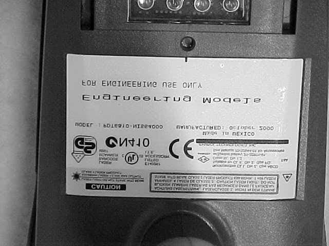
Click to zoom
Application Details
- Equipment Class
- DXX - Part 15 Low Power Communication Device Transmitter
- Date of Grant
- Mar 12, 2001
- Application Purpose
- Original Equipment
- Date of Application
- Mar 12, 2001
- Equipment Note
- Hand Held Portable Computer
- Frequency Range
- 2481.92000000 - 2481.92000000
- Company
- Symbol Technologies Inc
- Country
- United States
Documents & Files
Document Text
Text extracted from the exhibit documents filed with the FCC. Open a document above to read the original.
Users Manual
68XX Series + - = Status - 68XX Series 1998 - 1999 SYMBOL TECHNOLOGIES, INC. All rights reserved. Symbol reserves the right to make changes to any product to improve reliability, function, or design. Symbol does not assume any product liability arising out of, or in connection with, the application or use of any product, circuit, or application described herein. No license is granted, either expressly or by implication, estoppel, or otherwise under any patent right or patent, covering or relating to any combination, system, apparatus, machine, material, method, or process in which Symbol products might be used. An implied license only exists for equipment, circuits, and subsystems contained in Symbol products. Symbol, Spectrum One, and Spectrum24 are registered trademarks of Symbol Technologies, Inc. Other product names mentioned in this manual may be trademarks or registered trademarks of their respective companies and are hereby acknowledged. Symbol Technologies, Inc. One Symbol Plaza Holtsville, N.Y. 11742-1300 http://www.symbol.com Patents This product is covered by one or more of the following U.S. and foreign Patents: U.S. Patent No.4,360,798; 4,369,361; 4,387,297; 4,460,120; 4,496,831; 4,593,186; 4,603,262; 4,607,156; 4,652,750; 4,673,805; 4,736,095; 4,758,717; 4,816,660; 4,845,350; 4,896,026; 4,897,532; 4,923,281; 4,933,538; 4,992,717; 5,015,833; 5,017,765; 5,021,641; 5,029,183; 5,047,617; 5,103,461; 5,113,445; 5,130,520 5,140,144; 5,142,550; 5,149,950; 5,157,687; 5,168,148; 5,168,149; 5,180,904; 5,229,591; 5,230,088; 5,235,167; 5,243,655; 5,247,162; 5,250,791; 5,250,792; 5,262,627; 5,262,628; 5,266,787; 5,278,398; 5,280,162; 5,280,163; 5,280,164; 5,280,498; 5,304,786; 5,304,788; 5,306,900; 5,321,246; 5,324,924; 5,337,361; 5,367,151; 5,373,148; 5,378,882; 5,396,053; 5,396,055; 5,399,846; 5,408,081; 5,410,139; 5,410,140; 5,412,198; 5,418,812; 5,420,411; 5,436,440; 5,444,231; 5,449,891; 5,449,893; 5,468,949; 5,471,042; 5,478,998; 5,479,000; 5,479,002; 5,479,441; 5,504,322; 5,519,577; 5,528,621; 5,532,469; 5,543,610; 5,545,889; 5,552,592; 5,578,810; 5,581,070; 5,589,679; 5,589,680; 5,608,202; 5,612,531; 5,619,028; 5,664,229; 5,668,803; 5,675,139; 5,693,929; 5,698,835; 5,705,800; 5,714,746; 5,723,851; 5,734,152; 5,734,153; 5,745,794; 5,754,587; 5,762,516; 5,763,863; 5,767,500; 5,789,728; 5,808,287; 5,811,785; 5,811,787; 5,815,811; 5,821,519; 5,821,520; 5,823,812; 5,828,050; 5,850,078; D305,885; D341,584; D344,501; D359,483; D362,453; D363,700; D363,918; D370,478; D383,124; D391,250. Invention No. 55,358; 62,539; 69,060; 69,187 (Taiwan); No. 1,601,796; 1,907,875; 1,955,269 (Japan). European Patent 367,299; 414,281; 367,300; 367,298; UK 2,072,832; France 81/ 03938; Italy 1,138,713. rev. 1/99 1 Quick Reference Introduction The 68XX is a ruggedized, weather-resistant, hand-held portable computer combining the following capability in one package: • PC-standard architecture (8088 16-bit architecture) • DR-DOS compatibility • 16-line by 21-character display • Key input from 46-key alphanumeric keyboard • Integrated scanning capability • Sealed NiCd rechargeable or replaceable alkaline battery pack • Batch communications or RF network communications (with internally mounted antenna): -Spectrum One ® RF network (681X) -Spectrum24 ® RF network (684X). About This Guide This guide provides the operator with instructions for the following procedures: • Installing/removing the battery • Charging the battery • Powering the 68XX on and off • Adjusting the display contrast • Turning the backlight on/off • Using the keyboard • Using the integrated scanner • Running communications • Troubleshooting the 68XX. 2 68XX Series Parts of the 68XX + - = Status - Display Keyboard Scan LED Status LED Scan Window PWR Key Scan Trigger Battery Lock Handstrap Charging Contacts Optical Connectors Battery Compartment Battery Release Battery Pack 3 Quick Reference Required Accessories Required 68XX accessories include: • Five-cell, 780 mAh NiCd rechargeable battery pack or Six-cell, 600 mAh IS NiCd rechargeable battery pack • CCM 38/6860 4-slot charging and communication module with spare battery charging slot or • CRD 38/6865 1-slot cradle charging and communications cradle or • CRD 38/6866 4-slot charging and communications cradle • RS-232 serial cable(s) • Power supply (1 per cradle). Optional Accessories Optional 68XX accessories include: • Wall mounting kit (p/n 3866-000) • UBC battery charger (1000 or 2000) • PC adapter and printer interface module (PIM) • 10-hour trickle battery charger (wall cube) • Spectrum One and Spectrum24 network accessories •Holster. 4 68XX Series Providing Power Power for the 68XX is provided by a Nickel Cadmium (NiCd) rechargeable battery pack. Note: The Series 3800 NiCd battery packs, 3872-103, 3872- 105, and 3872-115, CANNOT be used in the 68XX. Installing New or Recharged NiCd Batteries To install the NiCd battery: 1. Orient the battery pack with the handle facing the 6800’s scan window. 2. Slide the pack into the battery compartment with the battery release buttons pressed in. 3. Press the battery lock in to secure. Changing the Battery Pack for the Intrinsically Safe PDT 68xx terminal To insert the battery pack: 1. Firmly insert the battery into the bottom of the terminal as shown in the following illustration. Battery Handle Battery Lock Release Button Battery Compartment Scan Window 5 Quick Reference 2. Use the enclosed battery locking key to lock the battery into place. As you are turning the locking key, the battery locking mechanism should be turning and locking the battery into place. 3. To unlock and remove the battery, use the battery locking key to unlock the battery locking mechanism, and pull the battery out of from the bottom of the terminal. Removing the NiCd Battery Pack 1. Press the battery release buttons on both sides of the handle. 2. Slide the battery pack out of the handle. Battery Locking Key Battery Locking Mechanism Press release button Press release button…
Text truncated - open the document above for the full version.
Block Diagram
2481.92MHz Printer Radio – Theory of Operation System Architecture: The radio is a half duplex OOK-modulated (On/Off Keying) heterodyned transceiver operating over a narrow band centered at 2481.92MHz. Operating only as a portable device, its antenna and ground plane are internal to the unit and inaccessible to users. Major functional blocks are listed below and a block diagram of their interconnection follows. A 1024MHz (doubled) synthesizer; A hybrid 433.92MHz OOK-modulated transmitter; A hybrid 433.92MHz OOK-demodulating receiver; A voltage clamp circuit (proprietary to Symbol); Up and down converters which implement the interface between the 2481.92MHz RF and the 433.92MHz hybrids; An RF Splitter which connects the RF transmit and receive signal paths with the antenna; Receive and transmit voltage regulators plus a voltage switch operating from a single 5V supply; And miscellaneous control logic and data inverter/level translators. . . Frequencies in the Block Diagram which are underlined and in bold typeface represent oscillators. There are no tunable sections in the transceiver. Frequency Synthesizer 1024MHz doubled TRANSMIT / RECEIVE∗ Hybrid 433.92MHz Transmitter Hybrid 433.92MHz Receiver RF Splitter Voltage Clamp A n t e n n a Data Translator - Inverter Data Translator - Inverter TXD RXD Down Converter Up Converter RADIO ENABLE∗ TRANSMIT VOLTAGE REGULATOR RECEIVE VOLTAGE REGULATOR VCC SWITCHED 2481.92 MHz 2481.92 MHz
Operational Description
2481.92MHz Printer Radio – Theory of Operation System Architecture: The radio is a half duplex OOK-modulated (On/Off Keying) heterodyned transceiver operating over a narrow band centered at 2481.92MHz. Operating only as a portable device, its antenna and ground plane are internal to the unit and inaccessible to users. Major functional blocks are listed below and a block diagram of their interconnection follows. A 1024MHz (doubled) synthesizer; A hybrid 433.92MHz OOK-modulated transmitter; A hybrid 433.92MHz OOK-demodulating receiver; A voltage clamp circuit (proprietary to Symbol); Up and down converters which implement the interface between the 2481.92MHz RF and the 433.92MHz hybrids; An RF Splitter which connects the RF transmit and receive signal paths with the antenna; Receive and transmit voltage regulators plus a voltage switch operating from a single 5V supply; And miscellaneous control logic and data inverter/level translators. . . Frequencies in the Block Diagram which are underlined and in bold typeface represent oscillators. There are no tunable sections in the transceiver. Frequency Synthesizer 1024MHz doubled TRANSMIT / RECEIVE∗ Hybrid 433.92MHz Transmitter Hybrid 433.92MHz Receiver RF Splitter Voltage Clamp A n t e n n a Data Translator - Inverter Data Translator - Inverter TXD RXD Down Converter Up Converter RADIO ENABLE∗ TRANSMIT VOLTAGE REGULATOR RECEIVE VOLTAGE REGULATOR VCC SWITCHED 2481.92 MHz 2481.92 MHz Power Supplies, Control Logic and Data The Printer Radio board is provided with a single 5V supply. This supply in turn provides power for the Receive Data Translator–Inverter and the Transmit and Receive Voltage regulators, and is connected through a P-channel MOSFET switch to the VCC Switched supply rail. The Receive Regulator supplies 3V to the 433.92MHz Hybrid Receiver. The VCC Switched rail, at +5V, powers the Voltage Clamp and the MC12179 IC in the Synthesizer. The 4V Transmit regulator powers the remaining circuitry, which includes the Transmit Data Translator–Inverter, Hybrid Transmitter, Up & Down Converter, and the VCO portion of the Frequency Synthesizer. Two control signals are supplied to the radio. The Radio Enable* signal simply activates or de-activates the radio power supplies. The Transmit/Receive* signal enables the Up Converter and disables the Down Converter in Transmit mode, and effects the reverse in Receive mode. The TXD and RXD signals are serial data streams connected to a standard 8 data bit, one start bit, one stop bit asynchronous UART. Bit rates can vary up to 19.2KbpS. Data Translator-Inverters These blocks are simple transistor circuits whose sole purpose is to provide logical signal inversion and a proper interface between the circuitry operating at different voltage levels at the DT-I inputs and outputs. Hybrid 433.92MHz Transmitter This is a simple On/Off oscillator running at the indicated frequency and keyed by the transmit Data Translator/Inverter. The oscillator is SAW-based, and thus is stable with temperature. 1024MHz (doubled) Frequency Synthesizer The 1024MHz (doubled) synthesizer is a PLL whose active components are an MC12179 frequency synthesizer and the VCO amplifier portion of the HP MX5001 up/down converter. Major passive components include a 4MHz crystal used by the MC12179 to generate the reference frequency, an RC loop filter, and the VCO resonating components (capacitors, an inductor, and a varactor). The MC12179 contains the amplifier portion of the crystal oscillator, a divide by 256 counter, and a phase comparator. The buffered output of the 4MHz crystal oscillator drives one input of the phase comparator, whose other leg is driven by the divide by 256 counter. The counter is fed by the VCO which is running at 1024MHz. To close the loop, the phase comparator drives the varactor through the R-C loop filter so as to set the varactor capacitance to resonate with the inductor and remaining capacitors at 1024MHz. The VCO frequency is doubled internally by the MX5001 to produce a 2048MHz signal which is applied to that chip’s mixer inputs. Up Converter The Up Converter consists of one of the two mixers found in the HP MX5001 IC. Enabled by the Transmit/Receive* control signal in transmit mode, the Up Converter mixes the outputs of the Frequency Synthesizer (doubled to 2048MHz) and the Transmitter Hybrid to produce a signal centered at 2481.92MHz. 2481.92MHz is the intentionally radiated frequency of this radio. RF Splitter The job of the passive RF Splitter is to provide an interface between the antenna, the Up Converter output and the Down Converter input. This interface provides sufficient filtering to minimize out of band (2481.92MHz) energy both radiated by and received through the antenna. Down Converter The Down Converter consists of one of the two mixers found in the HP MX5001 IC. Enabled by the Transmit/Receive* control signal in the receive mode, the Down Converter mixes the output of the Frequency Synthesizer (doubled to 2048MHz) with the 2481.92MHz signal received by the antenna. The intentional output of the Down Converter is centered at 433.92MHz. This signal is passed on to the Hybrid 433.92MHz Receiver. Hybrid 433.92MHz Receiver The Receiver is a homodyne. Manufactured by RF Monolithics, it incorporates a narrow band 433.92MHz SAW filter in its front end for RF selectivity. All of its pre-detector gain is provided at this frequency. Instability is precluded by a unique sampling design employing two cascaded and sequenced amplifiers. The first amplifier drives a SAW delay line and is turned on only for the time it takes a signal to propagate through the line. As the signal emerges from that line, the first amplifier is turned off and a second amplifier fed by the line is turned on. After the end of the sampled signal emerges from the second amplifier, that amplifier is turned off and the cycle repeats. Since the total amount of amplifier gain active at any one time is only the square root of the total ga…
Text truncated - open the document above for the full version.
Test Report
APPLICANT Symbol Technologies, Inc. One Symbol Plaza Holtsville, NY 11742 Manufacturer Symbol Technologies, Inc. One Symbol Plaza Holtsville, NY 11742 TEST SPECIFICATION:FCC Rules and Regulations Part 15, Subpart C TEST PROCEDURE:FCC 15.249(a) TEST SAMPLE DESCRIPTION BRANDNAME:Symbol MODEL:PDT6845FCC ID: H9PPDT6845 TYPE:2.48192 GHz Pulsed Transmitter FREQUENCY RANGE:2.48192 GHz POWER REQUIREMENTS:6 VDC derived from a rechargeable NICAD Battery TESTS PERFORMED - 15.209(a)Radiated Emissions, Spurious Case - 15.249(a)Radiated Emissions, Fundamental and Harmonics - 15.249(c)Occupied Bandwidth REPORT OF MEASUREMENTS Applicant:Symbol Technologies, Inc.. Device:Pulsed RF Transmitter FCC ID:H9PPDT6845 Power Requirements:6 VDC derived from a rechargeable NICAD Battery Applicable Rule Section:Part 15, Subpart C, Section 15.249 TEST RESULTS 15.209(a):Field strength of emissions from the intentional radiator operating in the 2.4 to 2.4835 GHz frequency band did not exceed 50 mV/m average for the fundamental and 500 uV/m average for harmonics. 15.249(b):Field strength readings were recorded at a distance of three meters from the Intentional Radiator unless otherwise specified. 15.249(c):Emissions radiated outside the specified frequency band except for harmonics, were attenuated by at least 50dB or to the emissions limits of 15.209, whichever was the lesser attenuation. 15.249(d):All measurements were taken utilizing a peak detector. The peak field strength did not exceed the average limits under any condition of modulation. Duty Cycle Information: Please see attached file named Timinginfo.doc SPECTRUM ANALYZER DESENSITIZATION CONSIDERATIONS Due to the nature of the emissions being measured, care was taken to ensure that the resolution bandwidth of the spectrum analyzer was adequate to provide accurate measurements. The following formula was utilized: The device has maximum data rate of 19.2 Kbps. Therefore a minimum pulse width is 1/max. data rate = 1/19.2 kHz = 52 microseconds. Setting pulse desensitization equal to zero and utilizing the minimum observed pulse width of 52μs yields a minimum required bandwidth of 12.8 kHz. FCC specified bandwidths of 100kHz and 1MHz were utilized below and above 1GHz, respectively. GENERAL NOTES 1.All user accessible controls were adjusted to produce maximum emissions. 2.The unit operates in the band of 2.4 to 2.4835 GHz band at a single frequency of 2.48192 GHz. 3.The frequency range was scanned from 30 MHz to 25 GHz. All emissions not reported were more than 10dB below the specified limit. EXHIBIT 4 Radiated Emissions, Spurious Case Para. 15.209(a) (Please see separate e-file attachment named RE Spurious.doc) EXHIBIT 4 Radiated Emissions, Fundamental & Harmonic Para. 15.249(a) (Please see separate e-file attachment named RE FundHarm.doc) EXHIBIT 4 Occupied Bandwidth Para. 15.249(c) (Please see separate e-file attachment named OccBw.pdf) EQUIPMENT LIST Radiated Emissions, Fundamental and Harmonics, 2.4-25GHz ENTypeManufacturerDescriptionModel No.Cal DateDue Date 062High Gain Horn AntennaMicrolab/FXR1.7 GHz - 2.6 GHzR638A10/11/200010/11/2001 063High Gain Horn AntennaMicrolab/FXR2.6 GHz-3.95 GHzS638A10/11/200010/11/2001 064High Gain Horn AntennaMicrolab/FXR3.95 GHz - 5.85 GHzH638A10/11/200010/11/2001 065High Gain Horn AntennaMicrolab/FXR5.85 GHz - 8.2 GHzC638A10/11/200010/11/2001 066High Gain Horn AntennaMicrolab/FXR8.2 GHz - 12.4 GHzX638A10/11/200010/11/2001 067Open Area Test SiteRetlif3 MeterRNY09/20/200009/20/2003 129DHigh Gain Horn AntennaMicrolab/FXR12.4 GHz - 18 GHzY638A10/11/200010/11/2001 129EHigh Gain Horn AntennaMicrolab/FXR18 GHz - 26.5 GHzK638A09/18/200009/18/2001 141Spectrum AnalyzerHewlett Packard100 Hz - 40 GHz8566B08/03/200002/03/2001 141AGraphics PlotterHewlett PackardN/A7470A03/08/200003/08/2001 141BQuasi-Peak AdaptorHewlett Packard100 Hz - 1 GHz85650A08/02/200002/02/2001 420AmplifierHewlett Packard2.0 GHz - 18 GHz11975A09/29/200009/29/2001 421Harmonic MixerHewlett Packard18 GHz - 26.5 GHz11970K09/29/200009/29/2001 543PreamplifierHewlett Packard1.0 GHz - 26.5 GHz8449B06/16/199906/16/2001 Radiated Emissions, Spurious Case, 30MHz-25GHz ENTypeManufacturerDescriptionModel No.Cal DateDue Date 062High Gain Horn AntennaMicrolab/FXR1.7 GHz - 2.6 GHzR638A10/11/200010/11/2001 063High Gain Horn AntennaMicrolab/FXR2.6 GHz-3.95 GHzS638A10/11/200010/11/2001 064High Gain Horn AntennaMicrolab/FXR3.95 GHz - 5.85 GHzH638A10/11/200010/11/2001 065High Gain Horn AntennaMicrolab/FXR5.85 GHz - 8.2 GHzC638A10/11/200010/11/2001 066High Gain Horn AntennaMicrolab/FXR8.2 GHz - 12.4 GHzX638A10/11/200010/11/2001 067Open Area Test SiteRetlif3 MeterRNY09/20/200009/20/2003 129DHigh Gain Horn AntennaMicrolab/FXR12.4 GHz - 18 GHzY638A10/11/200010/11/2001 129EHigh Gain Horn AntennaMicrolab/FXR18 GHz - 26.5 GHzK638A09/18/200009/18/2001 133Broadband Pre-AmplifierElectro-Metrics10 kHz - 1 GHz, 26dBBPA-100006/13/200006/13/2001 141Spectrum AnalyzerHewlett Packard100 Hz - 40 GHz8566B08/03/200002/03/2001 141AGraphics PlotterHewlett PackardN/A7470A03/08/200003/08/2001 141BQuasi-Peak AdaptorHewlett Packard100 Hz - 1 GHz85650A08/02/200002/02/2001 206B6.0 dB AttenuatorTexscan0 - 1.0 GHzFP-50 - 6 dB06/13/200006/13/2001 420AmplifierHewlett Packard2.0 GHz - 18 GHz11975A09/29/200009/29/2001 421Harmonic MixerHewlett Packard18 GHz - 26.5 GHz11970K09/29/200009/29/2001 523BiconilogElectro-Mechanics26 - 2000 MHz3142B06/08/200006/08/2001 543PreamplifierHewlett Packard1.0 GHz - 26.5 GHz8449B06/16/199906/16/2001 617Interference AnalyzerElectro-Metrics10 kHz - 1 GHzEMC-3001/17/200001/27/2001 Test Setup Photograph for Radiated Emissions Retlif Testing Laboratories R Data Sheet 1 of 4 Test Method: FCC Part 15 Subpart C Radiated Emissions, Fundamental & Harmonic Emissions Customer: Symbol Technologies Job No. R-8874-1 Test Sample: 2.48192GHz Transmitter Paragraph: 15.249 Model No.: PDT6845 FCC ID: H9PPDT6845 Operating Mode: Continuously Transmitting a 2.48192GHz Signal Technician: Peter Lananna Date: January 1…
Text truncated - open the document above for the full version.
Test Setup Photos
Test Setup Photograph for Radiated Emissions
Contact Information
Applicant
Qianlin Zhou(Regulatory Specialist)
Technical Contact
Retlif Testing LaboratoriesThomas J Schneider
[email protected]631 737-1500
795 Marconi Avenue · Ronkonkoma, New York · United States
Non-Technical Contact
Retlif Testing LaboratoriesMichelle White
[email protected]631 737-1500
Test Firm
Retlif Testing LaboratoriesMichael Bozza
Technical Specifications
| # | Rule Parts | Frequency Range | Power Output |
|---|---|---|---|
| 1 | 15C | 2.48 GHz - 2.48 GHz | - |
Other Applications from Symbol Technologies Inc

H9PCCHUB1
Jun 30, 2015Customer Concierge
Equipment Class
NII - Unlicensed National Information Infrastructure TX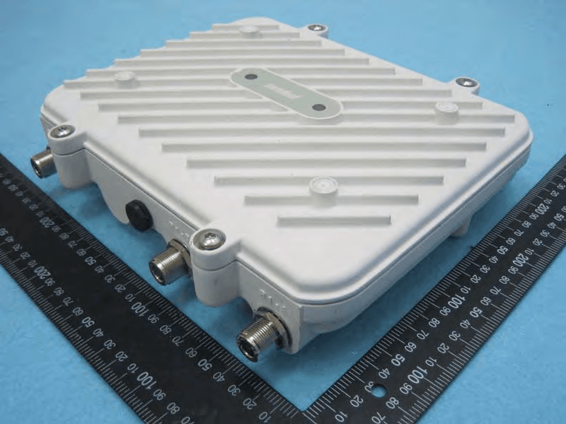
H9PAP7562
May 10, 2015802.11 abgn/ac Access Point
Equipment Class
DTS - Digital Transmission System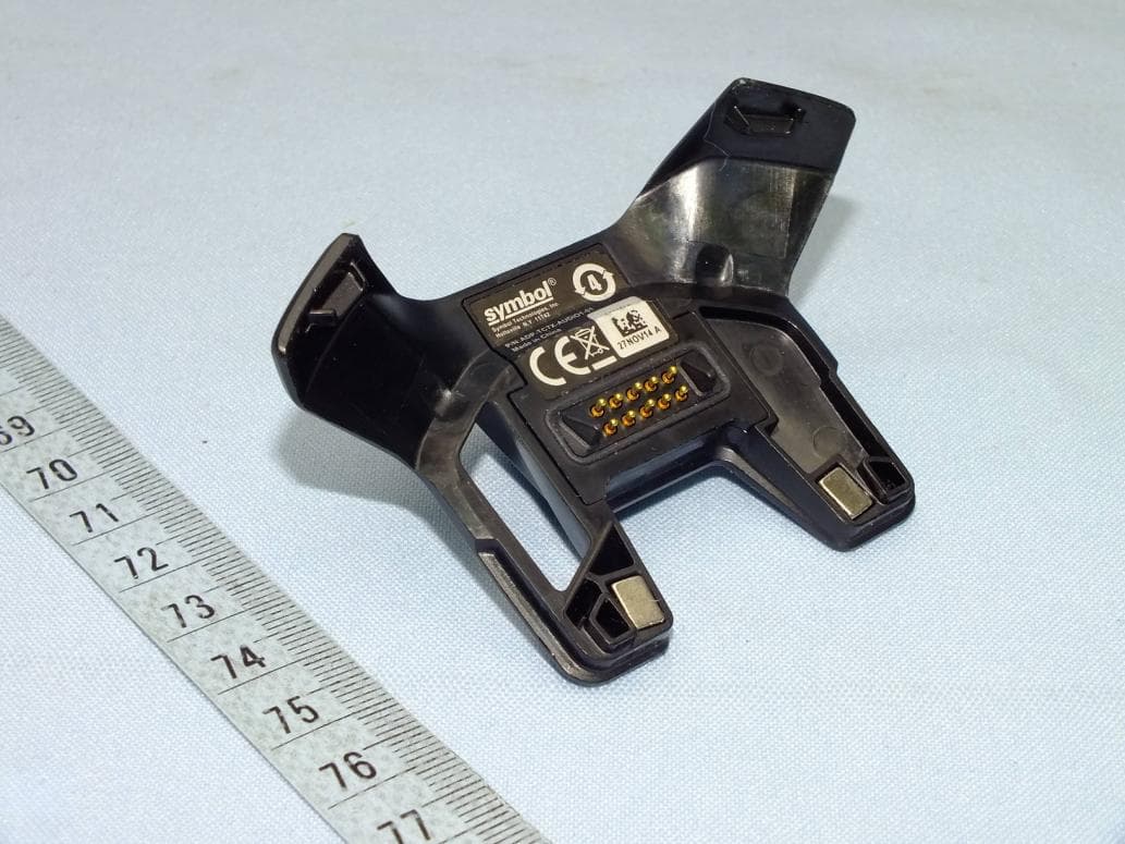
H9PTC75AH
Mar 26, 2015Touch Computer
Equipment Class
NII - Unlicensed National Information Infrastructure TX
H9PRA1202
Sep 24, 2014UHF Narrowband Radio Module
Equipment Class
TNB - Licensed Non-Broadcast Station Transmitter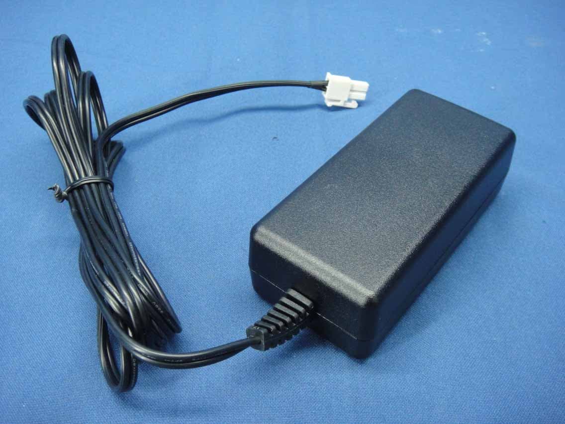
H9PEMG101
Aug 26, 2014802.15.4 Gateway
Equipment Class
DTS - Digital Transmission System