H9PPHASERMODULEPhaser Module
Symbol Technologies Inc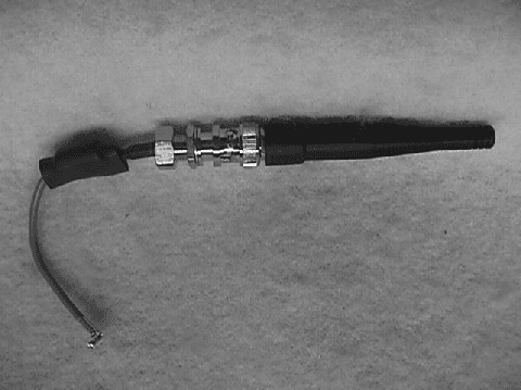
Click to zoom
Application Details
- Equipment Class
- DXX - Part 15 Low Power Communication Device Transmitter
- Date of Grant
- Oct 25, 2000
- Application Purpose
- Original Equipment
- Date of Application
- Sep 14, 2000
- Equipment Note
- Phaser Module
- Frequency Range
- 2402.00000000 - 2482.00000000
- Company
- Symbol Technologies Inc
- Country
- United States
Documents & Files
Document Text
Text extracted from the exhibit documents filed with the FCC. Open a document above to read the original.
Users Manual
The following regulatory information will be added to the final version of the Installation Guide. Regulatory Addendum Radio Frequency Interference Requirements This device has been tested and found to comply with the limits for a Class A digital device pursuant to Part 15 of the Federal Communications Rules and Regulation. These limits are designed to provide reasonable protection against harmful interference when the equipment is operated in a commercial environment. This equipment generates, uses, and can radiate radio frequency energy and, if not installed and used in accordance with the instruction manual, may cause harmful interference to radio communications. Operation of this equipment in a residential is likely to cause harmful interference in which case the user will be required to correct the interference at his own expense. However, there is no guarantee that interference will not occur in a particular installation. If the equipment does cause harmful interference to radio or television reception, which can be determined by turning the equipment off and on, the user is encouraged to try and correct the interference by one of the following measures: • Re-orient or relocate the receiving antenna. • Increase the separation between the equipment and receiver. • Connect the equipment into an outlet on a circuit different from that which the receiver is connected. • Consult the dealer or an experienced radio/TV technician for help. This device complies with FCC Part 15. Operation is subject to the following two conditions: (1) this device may not cause harmful interference and (2) this device must accept any interference received, including interference that may cause undesired operation.” Radio Frequency Interference Requirements- Canada This device complies with RSS 210 of Industry & Science Canada. Operation is subject to the following two conditions: (1) this device may not cause harmful interference and (2) this device must accept any interference received, including interference that may cause undesired operation.” This Class A digital apparatus meets the requirements of the Industry Canada Standard ICES-003. Cet appareil numerique de la Classe A est conforme a la norme NMB-003 du Canada. CE Marking and European Union Compliance Products intended for sale within the European Union are marked with the CE Mark which indicates compliance to applicable Directives and European Normes (EN), as follows, Amendments to these Directives or ENs are included: Applicable Directives • Electromagnetic Compatibility Directive 89/336/EEC • Low Voltage Directive 73/23/EEC Applicable Standards • EN 55022-Limits and Methods of Measurement of Radio Interference Characteristics of Information technology Equipment • EN 55024:1998; Information technology equipment-Immunity characteristics-Limits and methods of measurement. • IEC 1000-4-2(1995-01)-Electromagnetic Compatibility (EMC) – Part 4: Testing and measurement techniques-Section 2: Electrostatic Discharge immunity test. • IEC 1000-4-3(1995-03)-Electromagnetic Compatibility (EMC) –Part 4: Testing and measurement techniques-Section 3: Radiated, radio-frequency electromagnetic field immunity test. • IEC 1000-4-4(1995-01)-Electromagnetic Compatibility (EMC) –Part 4: Testing and measurement techniques-Section 4: E lectrical Fast transient /burst immunity test. • EN 60 950+Amd1 + Amd @-Safety of Information Technology Equipment Including Electrical Business Equipment • EN 60 825-1 (EN 60 825)- Safety of Devices Containing Lasers Laser Devices Symbol products using lasers comply with US 21 CFR1040.10, Subchapter J and IEC 825/EN 60 825 (or IEC 825-1/EN 60 825-1, depending on the date of manufacture). The laser classification is marked on one of the labels on the product. Class 1 Laser devices are not considered hazardous when used for their intended purpose. The following statement is required to comply with US and international regulations: Caution: Use of controls, adjustments or performance of procedures other than those specified herein may result in hazardous laser light exposure. Class 2 laser scanners use a low power visible light diode. As with any very bright light source such as the sun, the user should avoid staring directly into the light beam. Momentary exposure to a Class 2 laser is not known to be harmful. RF Devices Symbol’s RF products are designed to be compliant with the rules and regulations in the locations into which they are sold and will be labeled as required. The majority of Symbol’s RF devices are type approved and do not require the user to obtain license or authorization before using the equipment. Any changes or modifications to Symbol Technologies equipment not expressly approved by Symbol Technologies could void the user’s authority to operate the equipment. “Important Note: To comply with FCC and Industry Canada RF exposure requirements, this mobile device is approved for operation when there is 20 cm or more between the antenna and the user’s body.” .
Attestation Statements
Phaser RF Module - 24-42507-01 FCC ID:H9PPHASERMODULE These are the responses to the specific questions posed by the FCC for module approval: Note that we are applying for a limited modular approval since we do not comply with all module requirements. A limited modular approval is acceptable since Symbol Technologies will have complete control over all design and integration efforts. 1) The modular transmitter must have its own RF shielding. This is intended to ensure that the module does not have to rely upon the shielding provided by the device into which it is installed in order for all modular transmitter emissions to comply with Part 15 limits. It is also intended to prevent coupling between the RF circuitry of the module and any wires or circuits in the device into which the module is installed. Such coupling may result in non-compliant operation. The module contains its own RF shielding. A snap-on shield is attached to one side of the PCB shielding the VCO and other RF components. The module will pass all radiated emissions tests with this shield in place. 2) The modular transmitter must have buffered modulation/data inputs (if such inputs are provided) to ensure that the module will comply with Part 15 requirements under conditions of excessive data rates or over-modulation. The TXD data input to the module is buffered and thresholded with a comparator. This removes the voltage effects on the RF modulation. Data rate control is limited not by buffering on the TXD input, but the response time of the phase lock loop that produces the RF output. Other inputs to the module, such as the data signals to the synthesizer are CMOS inputs buffered internal to the synthesizer chip. Note that the module also requires a reference clock for the phase lock loop. The value of this clock must be 6.2Mhz ± ±± ± 22ppm. 3) The modular transmitter must have its own power supply regulation. This is intended to ensure that the module will comply with Part 15 requirements regardless of the design of the power supplying circuitry in the device into which the module is installed. The module does not have its own power supply regulation. Although a voltage regulator is present to provide power to the VCO and synthesizer circuitry, other parts of the design rely on a stable Vcc into the module. 4) The modular transmitter must comply with the antenna requirements of Section 15.203 and 15.204(c). The antenna must either be permanently attached or employ a “unique” antenna coupler (at all connections between the module and the antenna, including the cable). Any antenna used with the module must be approved with the module, either at the time of initial authorization or through a Class II permissive change. The “professional installation” provision of Section 15.203 may not be applied to modules. One variant of the module contains an integral, permanently attached antenna. The other variant, which uses an external antenna, contains a coaxial connection using a unique antenna coupler. 5) The modular transmitter must be tested in a stand-alone configuration, i.e., the module must not be inside another device during testing. This is intended to demonstrate that the module is capable of complying with Part 15 emission limits regardless of the device into which it is eventually installed. Unless the transmitter module will be battery powered, it must comply with the AC line conducted requirements found in Section 15.207. AC or DC power lines and data input/output lines connected to the module must not contain ferrites, unless they will be marketed with the module (see Section 15.27(a)). The length of these lines shall be length typical of actual use or, if that length is unknown, at least 10 centimeters to insure that there is no coupling between the case of the module and supporting equipment. Any accessories, peripherals, or support equipment connected to the module during testing shall be unmodified or commercially available (see Section 15.31(i)).an authorized module is installed must still be authorized as a PC peripheral, subject to the appropriate equipment authorization). The module submitted for test is a stand-alone module, with all signal and power lines attached to a connector. In order to exercise the module, it is connected to a host test box which contains a microprocessor that programs the transmit frequency and provides transmit data. No ferrites or other suppression components are present – the what you see is what you get. The goal of the modular approval is to copy the module PCB artwork (exact copy) and integrate it onto other PCB designs. During the integration, the module will clearly be separated by the absence of copper on all layers of the PCB and all signals will be routed to the module through a single “bridge” on the PCB. 6) The modular transmitter must be labeled with its own FCC ID number, and, if the FCC ID is not visible when the module is installed inside another device, then the outside of the device into which the module is installed must also display a label referring to the enclosed module. This exterior label can use wording such as the following: “Contains Transmitter Module FCC ID: XYZMODEL1” or “Contains FCC ID: XYZMODEL1.” Any similar wording that expresses the same meaning may be used. The Grantee may either provide such a label, an example of which must be included in the application for equipment authorization, or, must provide adequate instructions along with the module which explain this requirement. In the latter case, a copy of these instructions must be included in the application for equipment authorization. Symbol will comply. Sample label file shows correct wording. 7) The modular transmitter must comply with any specific rule or operating requirements applicable to the transmitter and the manufacturer must provide adequate instructions along with the module to explain any such requirements. A copy of these instructions must be included in the application for equi…
Text truncated - open the document above for the full version.
Block Diagram
BPF 2.4 - 2.5GHZ RX/TX SWITCH x IF BPF 10.7MHZ ±230KHZ IF SYSTEM Adjustable Amplifier VCO LOOP FILTER FREQ SYNTH + TX DATA FROM MICRO- PROCESSOR 3 6.2MHZ REFERENCE GENERATED BY MICROPROCESSOR LNALNA PA DATA SLICER RX DATA 2402 - 2480MHZ 10.7 MHZ BASEBAND (25KHZ) RX LO: 2412.7 - 2490.7 MHZ TX: 2402 - 2480 MHZ FM DEVIATION ADJUSTMENT TXV TXV* RXV SVCC SVCC RXV* TXV POWER SUPPLIES: TXV = LAST OUTPUT STAGE POWER (ACTUALLY TRANSMITTING) RXV = RECEIVER CIRCUIT POWER SVCC = +5V, POWER CIRCUITS COMMON TO TX AND RX SYMBOL TECHNOLOGIES PHASER RF MODULE 24-42507-01 SVCC MODULE INTERFACE: +5V GROUND VCC_ENABLE* TX_ENABLE* RX_ENABLE* SYNTHESIZER_DATA SYNTHESIZER_LATCH SYNTHESIZER_CLOCK SYNTHESIZER_REFERENCE RF_CARRIER_SENSE TRANSMIT_DATA RECEIVE_DATA
ID Label/Location Info
Sample FCC Label Symbol Technologies Inc. Contains Transmitter Module: FCC ID: H9PPHASERMODULE This device complies with Part 15 of the FCC rules. Operation is subject to the following two conditions: (1) this device may not cause harmful interference and (2) this device must accept any interference received, including interference that may cause undesired operation. This is a sample draft of the label that will be located on the underside of the product. Sandy Mazzola
Operational Description
Theory of Operation (Phaser RF Module) Symbol ConfidentialUnless marked otherwise, printed copies are uncontrolled Page 1 of 5 Theory of Operation: Phaser RF Module (24-42507-01) FCC ID:H9PPHASERMODULE 1. Purpose The purpose of this document and the respective schematic is to provide a description of the detailed design of the Phaser RF module. 2. References [1] Schematic: Phaser RF Module17-42507-01 3. Overview This document details the RF sections of the Phaser module. It is not intended to describe the in-depth details of component value selection and matching. Rather it is an overview of the radio architecture. 4. Module Interface The interface to the module consists of eleven signals. Four are for various power enables. RF_VCC_ENB* enables power to the radio, RF_TXV_ENB* enables power to the transmitter output stage U308, RF_RXV_ENB* enables power to the receiver, and RF_/RXV_ENB* which enables power to U305 (the first transmitter stage). See the figure at the end of this document for a timing diagram of a transmit/receive session. The next three, RF_SYNTH_DATA, RF_SYNTH_CLK, and RF_SYNTH_LATCH are used to serially program the frequency synthesizer on the radio. The synthesizer needs to be reprogrammed during each RF session because the PLL is used as a reference for both receive and transmit. Thus, it must change frequency by 10.7Mhz (the IF frequency) each time it switches between receive and transmit. For example, the synthesizer is programmed to 2402 MHz to transmit, after the data is transmitted the synthesizer is reprogrammed to 2412.7 MHz and set to receive to await an acknowledgment. The next signal is RF_SYNTH_REF. The RF synthesizer needs a reference clock to generate its timing and synchronization. The reference clock frequency must be either a sine wave or square wave at 6.2Mhz ±22ppm. Setting the synthesizer’s reference divide ratio to 62 allows the RF frequency to be resolved in 100 kHz steps (6.2 MHz/62 = 100 kHz). This will provide for the 10.7 MHz difference between TX and RX frequencies. The next two lines are RF_RXD, and RF_TXD. These are the raw received data from the radio and the desired transmit data to the radio, respectively. They are connected to a UART channel of a microprocessor. The baud rate used on this channel is 48 kbps. The last line is RF_CARR_SENS. This signal originates from a comparator on the radio’s RSSI line. It provides an indication about a received RF signal’s strength. It is used to alert the microprocessor that the receiver senses a strong carrier signal. So far this signal has not proved to be sensitive enough to be used reliably as an indicator of RF data. Theory of Operation (Phaser RF Module) Symbol ConfidentialUnless marked otherwise, printed copies are uncontrolled Page 2 of 5 5. Transmit Duty Cycle Limitations Since the transmit output power of the Phaser module exceeds 0dBm (1 milliwatt), a duty-cycle limitation must be placed on the transmission of data. This is done to keep the average transmit power within FCC specifications. The maximum transmit duty cycle for the Phaser RF module is 30%. This means that the module cannot transmit more than 30ms out of every 100ms interval. The duty cycle is controlled inherently by setting a maximum data frame size. The software that generates a frame imposes a limit of 30ms in total length. After the transmission, the software delays 70ms minimum to guarantee the 30% duty cycle. During actual transmission, a raw bit rate of 48kbps is transmitted. The transmit data is connected directly to a UART. 6. Radio Section The radio used in the Phaser design is based on the older Nomad (predecessor to Phaser) architecture, with many improvements. It is tuned for 50Kbps operation, using 81 1Mhz channels between 2.4GHz and 2.5GHz. Based on the standard single conversion super-heterodyne FM digital radio design, both the scanner and base contain transmit and receive sections designed to communicate half-duplex. 6.1 Transmit section To produce the FM signal at the desired RF channel frequency, the output from a VCO is directly modulated with the transmit data. The VCO (U310), working in conjunction with the RF synthesizer (U307) and low pass filter U312 to form a PLL. In an attempt to lock the VCO to a certain phase and frequency, U307 provides an error voltage, which becomes the VCOADJ signal. Once locked, the output of the VCO is a constant frequency. This frequency (the carrier) is set by the microprocessor via the three serial control signals (RF_SYNTH_DATA, RF_SYNTH_CLK, and RF_SYNTH_LATCH). The transmit data arrives at comparator U309 via the RF_TXD signal. The comparator’s output is directly coupled to the VCO error signal. Thus, as the data switches between 1 and 0, the frequency of the VCO shifts slightly around some middle frequency (the carrier). Note that if the data contained on RF_TXD contains too many consecutive 1’s or 0’s, the PLL will have time to correct and depth of modulation reduces to zero. Thus, the radio has certain limitations on the transmit data, discussed in the later section. Resistor R322 controls the amount of “pull” the transmit data has on the VCO, thus controlling the FM deviation (or modulation). The VCO output is passed through two stages of RF amplifiers and enters the RF switch, U302. In transmit mode, this switch is set to pass the output signal through the filter FL301 and onto the antenna. The nominal output power is 8dBm, at the antenna connector. 6.2 Receive section The incoming RF signal arrives at the antenna and passes through a band pass filter FL301. In receive mode, the RF signal passes through an RF switch and two stages of high gain RF amplifiers (U302, U303 & U304). Then it enters a mixer (U306) which down converts the signal to the IF frequency of 10.7Mhz. Note that the previously discussed VCO is used to mix with the incoming RF signal. Thus, the microprocessor sets the synthesizer (U307) to 10.7Mhz above the desired receive frequency. The IF signal …
Text truncated - open the document above for the full version.
Parts List/Tune Up Info
Symbol Technologies Phaser RF Module 24-42507-01 STUFF LIST - 1 CAP-0.01UF,10%,X7R,16V,0402 50-11515-103 C310 CAP-0.01UF,10%,X7R,16V,0402 50-11515-103 C318 CAP-0.01UF,10%,X7R,16V,0402 50-11515-103 C323 CAP-0.01UF,10%,X7R,16V,0402 50-11515-103 C339 CAP-0.01UF,10%,X7R,16V,0402 50-11515-103 C341 CAP-0.01UF,10%,X7R,16V,0402 50-11515-103 C344 CAP-0.01UF,10%,X7R,16V,0402 50-11515-103 C346 CAP-0.01UF,10%,X7R,16V,0402 50-11515-103 C357 CAP-0.01UF,10%,X7R,16V,0402 50-11515-103 C358 CAP-0.01UF,10%,X7R,16V,0402 50-11515-103 C359 CAP-0.01UF,10%,X7R,16V,0402 50-11515-103 C371 CAP-0.01UF,10%,X7R,16V,0402 50-11515-103 C390 ---------------- CAP-0.01UF,10%,X7R,50V,0603 50-11512-103 C309 CAP-0.01UF,10%,X7R,50V,0603 50-11512-103 C348 CAP-0.01UF,10%,X7R,50V,0603 50-11512-103 C351 CAP-0.01UF,10%,X7R,50V,0603 50-11512-103 C363 CAP-0.01UF,10%,X7R,50V,0603 50-11512-103 C388 ---------------- CAP-0.1UF,10%,X7R,16V,0603 50-11517-104 C302 ---------------- CAP-1.2PF,5%,COG,50V,0603 50-11509-1R2 C312 CAP-1.2PF,5%,COG,50V,0603 50-11509-1R2 C321 ---------------- CAP-1000PF,5%,X7R,50V,0603 50-11511-102 C334 CAP-1000PF,5%,X7R,50V,0603 50-11511-102 C389 ---------------- CAP-100PF,5%,COG,50V,0603 50-11509-101 C313 CAP-100PF,5%,COG,50V,0603 50-11509-101 C364 ---------------- CAP-1200PF,5%,COG,50V,0603 50-11511-122 C342 CAP-1200PF,5%,COG,50V,0603 50-11511-122 C345 ---------------- CAP-120PF,1%,COG,50V,0603 50-11513-121 C350 ---------------- CAP-180PF,5%,COG,50V,0603 50-11509-181 C305 ---------------- CAP-1UF,Z%,Y5V,16V,0805 50-21500-005 C324 CAP-1UF,Z%,Y5V,16V,0805 50-21500-005 C349 CAP-1UF,Z%,Y5V,16V,0805 50-21500-005 C356 CAP-1UF,Z%,Y5V,16V,0805 50-21500-005 C360 ---------------- CAP-22PF,5%,COG,25V,0402 50-11514-220 C343 CAP-22PF,5%,COG,25V,0402 50-11514-220 C367 ---------------- CAP-22PF,5%,COG,50V,0603 50-11509-220 C304 CAP-22PF,5%,COG,50V,0603 50-11509-220 C306 CAP-22PF,5%,COG,50V,0603 50-11509-220 C307 CAP-22PF,5%,COG,50V,0603 50-11509-220 C311 CAP-22PF,5%,COG,50V,0603 50-11509-220 C314 CAP-22PF,5%,COG,50V,0603 50-11509-220 C316 CAP-22PF,5%,COG,50V,0603 50-11509-220 C317 CAP-22PF,5%,COG,50V,0603 50-11509-220 C320 CAP-22PF,5%,COG,50V,0603 50-11509-220 C325 ---------------- CAP-3.3PF,5%,COG,50V,0603 50-11509-3R3 C326 ---------------- CAP-33PF,5%,COG,50V,0603 50-11509-330 C308 CAP-33PF,5%,COG,50V,0603 50-11509-330 C319 ---------------- CAP-390PF,5%,COG,50V,0603 50-11509-391 C362 ---------------- CAP-4.7PF,5%,COG,50V,0603 50-11509-4R7 C303 ---------------- CAP-56PF,5%,COG,25V,0402 50-11514-560 C337 ---------------- FDC6306P-FDC6306P 50-24800-035 Q302 FDC6306P-FDC6306P 50-24800-035 Q303 ---------------- INDUCTOR-1.2UH,0805 50-21803-1R2 L326 ---------------- INDUCTOR-1.5UH,SMD_LQS33 50-21806-1R5 L311 ---------------- INDUCTOR-1.8NH,0603 50-11801-1R8 L323 ---------------- INDUCTOR-2.7NH,0603 50-11801-2R7 L308 ---------------- INDUCTOR-22NH,0603 50-11801-220 L304 INDUCTOR-22NH,0603 50-11801-220 L307 INDUCTOR-22NH,0603 50-11801-220 L324 INDUCTOR-22NH,0603 50-11801-220 L325 ---------------- INDUCTOR-3.3NH,0603 50-11801-3R3 L306 INDUCTOR-3.3NH,0603 50-11801-3R3 L309 INDUCTOR-3.3NH,0603 50-11801-3R3 L322 ---------------- INDUCTOR-BEAD,1206 50-11800-007 L310 ---------------- J-1S-S1HDINS-76D 50-12100-621 J301 J-1S-S1HDINS-76D 50-12100-621 J305 J-1S-S1HDINS-76D 50-12100-621 J306 ---------------- J-1S-SLT30X140 PART_OF_PCB J307 J-1S-SLT30X140 PART_OF_PCB J308 J-1S-SLT30X140 PART_OF_PCB J309 J-1S-SLT30X140 PART_OF_PCB J310 ---------------- LFSN30-LFSN30 50-22700-017 FL301 ---------------- LM358-SO8 50-03130-177 U312 ---------------- LMX2325-TSSOP20 50-13130-470 U307 ---------------- LP2982-LP2982_4V 50-13130-618 U314 ---------------- MGA81563-SOT363 50-23450-023 U308 ---------------- MGA87563-SOT363 50-23450-021 U303 MGA87563-SOT363 50-23450-021 U304 ---------------- NPN-MMBT3904WT1,SOT323 50-24800-022 Q300 ---------------- PCAP-0.47UF,16V,5%,TANT 50-01500-251 C365 ---------------- PCAP-2.2UF,6.3V,10%,TANT_A 50-11523-225A6R3 C366 ---------------- PCAP-4.7UF,10V,20%,TANT 50-11524-475A010 C361 ---------------- RES-0,5%,1_16W,0603 50-14701-000 R312 ---------------- RES-1.5K,5%,1_16W,0402 50-14707-152 R326 ---------------- RES-10,5%,1_16W,0402 50-14707-100 R306 RES-10,5%,1_16W,0402 50-14707-100 R307 ---------------- RES-10,5%,1_16W,0603 50-14701-100 R303 RES-10,5%,1_16W,0603 50-14701-100 R345 RES-10,5%,1_16W,0603 50-14701-100 R425 ---------------- RES-10K,1%,1_16W,0603 50-14702-1002 R319 RES-10K,1%,1_16W,0603 50-14702-1002 R327 RES-10K,1%,1_16W,0603 50-14702-1002 R328 ---------------- RES-180,5%,1_16W,0402 50-14707-181 R351 ---------------- RES-180,5%,1_16W,0603 50-14701-181 R308 ---------------- RES-1K,1%,1_16W,0603 50-14702-1001 R305 RES-1K,1%,1_16W,0603 50-14702-1001 R315 RES-1K,1%,1_16W,0603 50-14702-1001 R325 RES-1K,1%,1_16W,0603 50-14702-1001 R342 RES-1K,1%,1_16W,0603 50-14702-1001 R343 RES-1K,1%,1_16W,0603 50-14702-1001 R344 RES-1K,1%,1_16W,0603 50-14702-1001 R428 ---------------- RES-1K,5%,1_16W,0402 50-14707-102 R320 ---------------- RES-2.2K,5%,1_16W,0402 50-14707-222 R350 ---------------- RES-3.3K,5%,1_16W,0603 50-14701-332 R347 RES-3.3K,5%,1_16W,0603 50-14701-332 R348 RES-3.3K,5%,1_16W,0603 50-14701-332 R349 ---------------- RES-33,5%,1_16W,0603 50-14701-330 R332 RES-33,5%,1_16W,0603 50-14701-330 R338 ---------------- RES-33K,5%,1_16W,0603 50-14701-333 R321 ---------------- RES-4.7K,5%,1_16W,0402 50-14707-472 R302 ---------------- RES-4.7K,5%,1_16W,0603 50-14701-472 R334 RES-4.7K,5%,1_16W,0603 50-14701-472 R336 ---------------- RES-47,5%,1_16W,0603 50-14701-470 R309 ---------------- RES-470,5%,1_16W,0402 50-14707-471 R352 ---------------- RES-470,5%,1_16W,0603 50-14701-471 R333 ---------------- RES-47K,5%,1_16W,0603 50-14701-473 R329 ---------------- RES-5.6K,5%,1_16W,0603 50-14701-562 R318 ---------------- RES-51,5%,1_16W,0402 50-14707-510 R310 ---------------- RES-51,5%,1_16W,0603 50-14701-510 R330 ---------------- RES-51K,5%,1_16W,0402 50-14707-513 R324 RES-51K,5%,1_16W,0402 50-14707-513 R331 ---------------- RES-62,5%,1_1…
Text truncated - open the document above for the full version.
Test Report
APPLICANT Symbol Technologies, Inc. One Symbol Plaza Holtsville, NY 11742 Manufacturer Symbol Technologies, Inc. One Symbol Plaza Holtsville, NY 11742 TEST SPECIFICATION:FCC Rules and Regulations Part 15, Subpart C TEST PROCEDURE:FCC 15.249(a) TEST SAMP LE DESCRIP TION BRANDNAME:Symbol PART NUMBER:24-42507-01FCC ID: H9PPHASERMODULE TYPE:2.4 GHz Pulsed RF Transmitter Module FREQUENCY RANGE:2402 to 2482 MHz POWER REQUIREMENTS: +5 VDC derived from Host Terminal TESTS P ERFORMED - 15.207(a)Conducted Emissions, 450 kHz to 30 MHz - 15.209(a)Radiated Emissions, Spurious Case - 15.249(a)Radiated Emissions, Fundamental and Harmonics - 15.249(c)Occupied Bandwidth REPORT OF MEASUREMENTS Applicant:Symbol Technologies, Inc. Device:Pulsed RF Transmitter Module FCC ID:H9PPHASERMODULE Power Requirements:+5 VDC derived from the Host Terminal Applicable Rule Section:Part 15, Subpart C, Section 15.249 TEST RESULTS 15.249(a):Field strength of emissions from the intentional radiator operating in the 2400-2483.5 MHz frequency band did not exceed 50 mV/m average for the fundamental and 500 uV/m average for harmonics. 15.249(b):Field strength readings were recorded at a distance of three meters from the Intentional Radiator unless otherwise specified. 15.249(c):Emissions radiated outside the specified frequency band except for harmonics, were attenuated by at least 50dB or to the emissions limits of 15.209, whichever was the lesser attenuation. 15.249(d):All measurements were taken utilizing a peak detector. The peak field strength did not exceed the average limits under any condition of modulation. GENERAL NOTES 1.All user accessible controls were adjusted to produce maximum emissions. 2.The unit operates in the band of 2400 to 2483.5 MHz. 3.The frequency range was scanned from 30 MHz to 25 GHz. All emissions not reported were more than 20dB below the specified limit. 4. See Attestation Statements for modular approval requirements. EXHIBIT 4 Radiated Emissions, Spurious Case Para. 15.209(a) (Please see separate e-file attachments named: integ spur.pdf, patch spur.pdf & whip spur.pdf) EXHIBIT 4 Radiated Emissions, Fundamental & Harmonic Para. 15.249(a) (Please see separate e-file attachments named: integ fund harm.pdf, patch fund harm.pdf & whip fund harm.pdf) EXHIBIT 4 Occupied Bandwidth Para. 15.249(c) (Please see separate e-file attachment named CEdata.pdf) EXHIBIT 4 Occupied Bandwidth Para. 15.249(c) (Please see separate e-file attachment named OccBw.pdf) EQUIPMENT LIST FCC Part 15, Subpart C, Paragraph 15.207 AC Line Conducted Emissions, 450 kHz to 30 MHz ENTypeManufacture rDe scriptionMode l No.Cal Date Due Date 076LISNSolar Electronics10 kHz - 30 MHz8012-50-R-24BNC01/12/200001/12/2001 7016EMC AnalyzerHewlett Packard9kHz - 1.8GHz8591EM02/18/200002/18/2001 7017Transient Limite rHe wle tt P a c k a rd9 k Hz - 200MHz11947A04/25/200004/25/2001
Test Report
Retlif Testing Laboratories R Data Sheet 1 of 4 Test Method: FCC Part 15 Subpart C Radiated Emissions, Fundamental & Harmonic Emissions Customer: Symbol Technologies Job No. R-8637-1 Test Sample: Pulsed RF Transmitter with integrated antenna. Paragraph: 15.249 Model No.: N/A FCC ID: H9PPHASERMODULE Operating Mode: Continuously Transmitting a 2.402GHz Signal Technician: Peter Lananna Date: August 22, 2000 Notes: Test Distance: 3 Meters Detector: Peak, Unless otherwise specified Test Freq. Antenna Pol./Height EUT Orientation Meter Reading Correction Factor Corrected Reading Converted Reading Peak Limit MHz (V/H)/Meters X / Y / Z dBuV dB dBuV/m uV/m uV/m 2402 H / 1.5 X 50.4 36.6 87.0 22387.2 500000 | H / 3.0 Y 55.6 36.6 92.2 40738.0 | | H / 1.1 Z 59.8 36.6 96.4 66069.3 | | V / 1.3 X 52.2 36.6 88.8 27542.3 | | V / 1.8 Y 45.7 36.6 82.3 13031.7 | 2402 V / 1.1 Z 48.2 36.6 84.8 17378.0 500000 4804 H / 1.1 X 53.7 -4.1 49.6 302.0 5000 | H / 1.1 Y 62.5 -4.1 58.4 831.8 | | H / 1.0 Z 56.1 -4.1 52.0 398.1 | | V / 1.0 X 53.0 -4.1 48.9 278.6 | | V / 1.0 Y 48.1 -4.1 44.0 158.5 | 4804 V / 1.0 Z 62.9 -4.1 58.8 871.0 5000 7206 H / 1.0 X 46.7 -2.0 44.7 171.8 5000 | H / 1.0 Y 50.7 -2.0 48.7 272.3 | | H / 1.0 Z 49.9 -2.0 47.9 248.3 | | V / 1.0 X 48.3 -2.0 46.3 206.5 | | V / 1.0 Y 47.7 -2.0 45.7 192.8 | 7206 V / 1.0 Z 52.1 -2.0 50.1 319.9 5000 9608 H / 1.0 X 44.2 -1.9 42.3 130.3 5000 | H / 1.0 Y 45.9 -1.9 44.0 158.5 | | H / 1.0 Z 50.3 -1.9 48.4 263.0 | | V / 1.0 X 46.5 -1.9 44.6 169.8 | | V / 1.0 Y 47.3 -1.9 45.4 186.2 | 9608 V / 1.0 Z 49.8 -1.9 47.9 248.3 5000 12010 H / 1.0 X 40.0 3.8 43.8 154.9* 5000 | H / 1.0 Y 40.0 3.8 43.8 154.9* | | H / 1.0 Z 40.0 3.8 43.8 154.9* | | V / 1.0 X 40.0 3.8 43.8 154.9* | | V / 1.0 Y 40.0 3.8 43.8 154.9* | 12010 V / 1.0 Z 40.0 3.8 43.8 154.9* 5000 The frequency range was scanned from 30 MHz to 25 GHz. All emissions not recorded were more Than 10 dB below the specified limit. Emissions from the EUT do not exceed the specified limits. *=Noise Floor Measurements (Minimum system sensitivity) Retlif Job Number R-8637-1 Retlif Testing Laboratories R Data Sheet 2 of 4 Test Method: FCC Part 15 Subpart C Radiated Emissions, Fundamental & Harmonic Emissions Customer: Symbol Technologies Job No. R-8637-1 Test Sample: Pulsed RF Transmitter with integrated antenna. Paragraph: 15.249 Model No.: N/A FCC ID: H9PPHASERMODULE Operating Mode: Continuously Transmitting a 2.402 GHz Signal Technician: Peter Lananna Date: August 22, 2000 Notes: Test Distance: 3 Meters **= Readings taken at 1 meter, correction factor includes distance extrapolation. Detector: Peak, unless otherwise specified Test Freq. Antenna Pol./Height EUT Orientation Meter Reading Correction Factor Corrected Reading Converted Reading Peak Limit MHz (V/H)-Meters X / Y / Z dBuV dB dBuV/m uV/m uV/m 14410 H / 1.0 X 35.0 10.8 45.8 195.0* 5000 | H / 1.0 Y 35.0 10.8 45.8 195.0* | | H / 1.0 Z…
Text truncated - open the document above for the full version.
Contact Information
Applicant
Qianlin Zhou(Regulatory Specialist)
Technical Contact
Retlif Testing LaboratoriesThomas J Schneider
[email protected]631-737-1500
795 Marconi Avenue · Ronkonkoma, New York · United States
Non-Technical Contact
Retlif Testing LaboratoriesMichelle White
[email protected]631-737-1500
Technical Specifications
| # | Rule Parts | Frequency Range | Power Output |
|---|---|---|---|
| 1 | 15C | 2.40 GHz - 2.48 GHz | - |
Other Applications from Symbol Technologies Inc

H9PCCHUB1
Jun 30, 2015Customer Concierge
Equipment Class
NII - Unlicensed National Information Infrastructure TX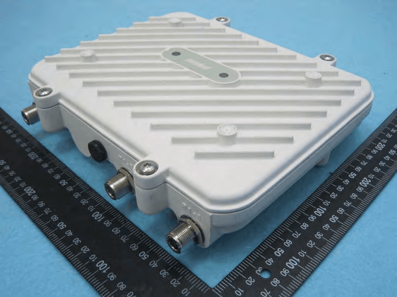
H9PAP7562
May 10, 2015802.11 abgn/ac Access Point
Equipment Class
DTS - Digital Transmission System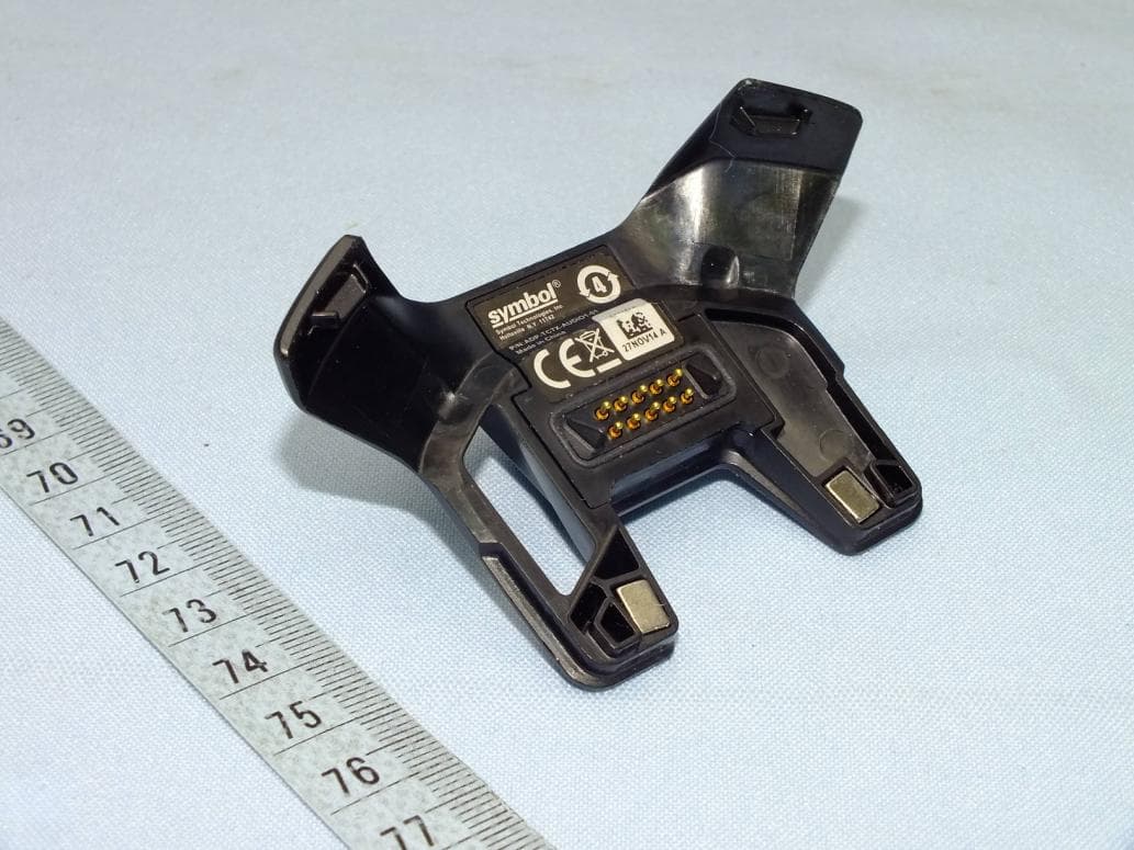
H9PTC75AH
Mar 26, 2015Touch Computer
Equipment Class
NII - Unlicensed National Information Infrastructure TX
H9PRA1202
Sep 24, 2014UHF Narrowband Radio Module
Equipment Class
TNB - Licensed Non-Broadcast Station Transmitter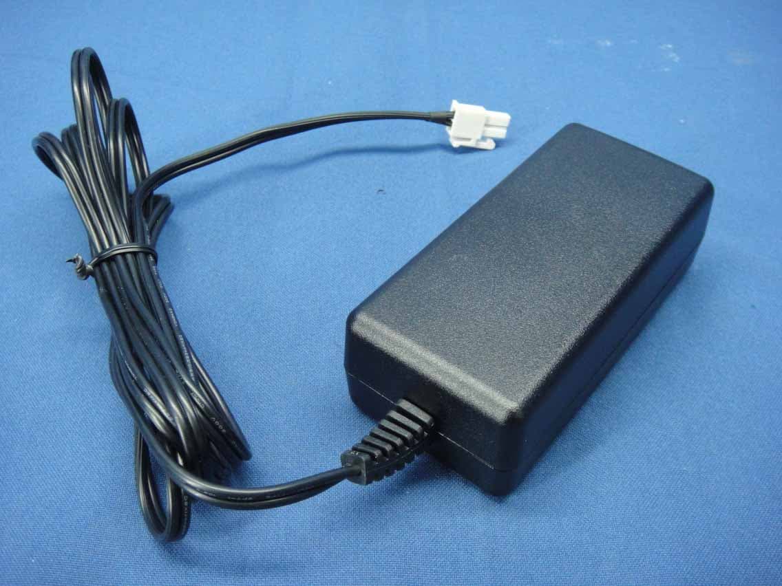
H9PEMG101
Aug 26, 2014802.15.4 Gateway
Equipment Class
DTS - Digital Transmission System