H9PWWC1049AWSS 1000 Wearable Data Entry System
Symbol Technologies Inc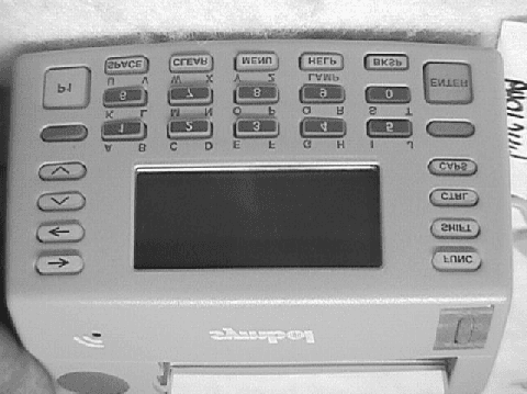
Click to zoom
Application Details
- Equipment Class
- DXX - Part 15 Low Power Communication Device Transmitter
- Date of Grant
- Dec 13, 2000
- Application Purpose
- Original Equipment
- Date of Application
- Sep 27, 2000
- Equipment Note
- WSS 1000 Wearable Data Entry System
- Frequency Range
- 916.00000000 - 916.00000000
- Company
- Symbol Technologies Inc
- Country
- United States
Documents & Files
Document Text
Text extracted from the exhibit documents filed with the FCC. Open a document above to read the original.
Users Manual
WSS 1000 System WSS 1000 System 1999-2000 SYMBOL TECHNOLOGIES, INC. All rights reserved. Symbol reserves the right to make changes to any product to improve reliability, function, or design. Symbol does not assume any product liability arising out of, or in connection with, the application or use of any product, circuit, or application described herein. No license is granted, either expressly or by implication, estoppel, or otherwise under any patent right or patent, covering or relating to any combination, system, apparatus, machine, material, method, or process in which Symbol products might be used. An implied license only exists for equipment, circuits, and subsystems contained in Symbol products. Symbol and the Symbol logo are registered trademarks of Symbol Technologies, Inc. Other product names mentioned in this manual may be trademarks or registered trademarks of their respective companies and are hereby acknowledged. Symbol Technologies, Inc. One Symbol Plaza Holtsville, N.Y. 11742-1300 http://www.symbol.com Quick Reference 1 Introduction The WSS 1000 is a wearable data entry system consisting of a laser bar code scanner, usually worn on the operator’s fingers or back of hand, and a wrist computer (WWC 1000) worn on the operator’s forearm. The detachable components work equally well for right- and left-handed individuals. Detachable personal mounts allow multiple operators to share both scanner and wrist computer without having to use the same mount. About This Guide This guide presents information on system components, assembling the WWC 1000, battery installation and charging, attaching the system, using the keyboard, and disassembly for use by others. For wearable scanner information, refer to the WSS 1000 Product Reference Guide , or the Quick Reference Guide provided with your scanner. 2 WSS 1000 System Parts of the WSS 1000 System Keyboard Display Speaker Battery Latch Power Switch Battery Charging Contacts Lithium-Ion Battery WWC 1000 Top WWC 1000 (Wrist Computer) Front Adjustable Straps Snap-On Bar WWC 1000 Wrist Mount Quick Reference 3 Installing and Charging the Battery The wrist computer and scanner are powered by a Lithium-Ion battery pack. The pack provides power for a typical 8-hour shift. Note: Before using the wrist computer, install and fully charge the Lithium-Ion battery pack. To install the battery pack in the WWC 1000: 1. Insert the battery pack, base first, in the battery compartment. 2. Line up the pack’s locking mechanism with the notch in the battery compartment wall by sliding the battery latch, and press the pack into place. 3. Release the battery latch to lock in place. Battery Latch Notch Battery Compartment Battery Pack Base 4 WSS 1000 System Charging the Battery in WWC 1000 To charge the Lithium-Ion battery in the WWC 1000: 1. Place the WWC 1000 in the cradle as shown be- low: 2. The cradle’s CHARGING light illuminates (RED) if the WWC 1000 is properly seated and the bat- tery is charging. 3. The battery requires approximately 2 hours to charge fully. The CHARGING light changes to GREEN when the battery is fully charged. 4. To remove the WWC 1000 from the cradle, tilt the WWC 1000 upward and pull out. For more information on the CS 1000 Cradle, re- fer to the CS 1000 Single-Slot Cradle QRG , p/n 70-16237-xx, or the CS 1000 4-Slot Cradle QRG , p/n 70-17661-xx. Quick Reference 5 Charging the Spare Battery Spare battery packs can be charged separate from the WWC 1000. To charge a spare battery pack in the cradle: 1. Insert the pack in the cradle’s spare charging slot. 2. The CHARGING light illuminates red. 3. The spare pack is charged in approximately two hours, even if the WWC 1000 is charging at the same time. The CHARGING light changes to green when the battery is fully charged. 6 WSS 1000 System Assembling the WSS 1000 System To assemble the WWC 1000 (wrist computer): 1. Place the WWC 1000 wrist computer onto the wrist mount, facing you. Be sure the mount is ori- ented so that the longer strap will be further up the forearm. 2. Snap the bar over the WWC 1000 using the snaps on either side of the mount. The straight part of the bar should lay across the front of the WWC 1000; the curved part in back. Quick Reference 7 Note: The snaps on the wrist mount act as a tear- away device allowing the wrist computer to detach from the mount if it catches on an object. 3. Plug the cable connector from the WWC 1000 in the interface port on the back of the scanner. 4. Place the WWC 1000 on your arm: a. Slide the wrist mount on your arm, so that the WWC 1000 wrist computer faces you. 8 WSS 1000 System b. Pull the straps through the buckles so the wrist mount is secure but not tight. c. Use the Velcro to secure the straps. 5. Assemble and mount your scanner. See your scan- ner’s Quick Reference Guide , or the WSS 1000 Product Reference Guide . Quick Reference 9 Powe r Once the battery pack is fully charged, you are ready to use the wrist computer. To power the wrist computer on, press the power switch on top of the WWC 1000. Display Light and Contrast To turn the display light and keypad backlight on, press LAMP ( Left Alpha and Help ). To adjust the contrast: •press FUNC and SPACE to darken the contrast, •press FUNC and BKSP to lighten the contrast. 10 WSS 1000 System Communicating with the Host Using the Cradle The CS 1000 cradle is used to perform communications with a host PC. To set up the cradle for operation: 1. Plug one end of a null modem cable (p/n 59846- 03-00) into the communications port located on the left end of the cradle. 2. Connect the other end of the cable to the host com- puter’s serial (COMM) port. 3. Provide power to the cradle by plugging the power supply’s round connector into the power port on the cradle and the other end of the power cable in an electrical outlet. 4. Insert the WWC 1000 in the cradle (the ring scan- ner can be attached). 5. Start the communications program as detailed in the WSS 1000 Product Reference Guide . Radio Co…
Text truncated - open the document above for the full version.
Block Diagram
Document Number 71-40735-01 916.5MHz Short Range Radio (with RFM TR1000 IC) – Theory of Operation Symbol Confidential Page 1 of 6 REVISIONS REVDESCRIPTIONDATEAPPROVED A 916.5MHz Short Range Radio (with RFM TR1000 IC) – Theory of Operation Author: Chris Paul Document Number 71-40735-01 916.5MHz Short Range Radio (with RFM TR1000 IC) – Theory of Operation Symbol Confidential Page 2 of 6 BLOCK DIAGRAM: 916.5MHz Short Range Radio (with RFM TR1000 IC ) RADIO DESCRIPTION The radio is a half duplex OOK-modulated (On/Off Keyed) homodyne transceiver operating over a narrow band centered at 916.5MHz. Operating only as a portable device, its antenna and ground plane are internal to the unit in which it is installed and therefore inaccessible to users. Its major functional blocks are listed below (please refer to the block diagram above.) An antenna; A Hybrid 916.5MHz Transceiver (TR1000) A data-slicing comparator preceded by a filter; A 3.0V linear voltage regulator plus a voltage switch operating from a single 5V supply (both of which can be enabled or disabled by the externally provided RAD_EN signal); And logic gates. PTT (low to TX, hi to RX) Filter and Comparator A n t e n n a Logic Gates RF_TXD RF_RXD RAD_EN* (low for radio on) +3V Linear Regulator +5V slow turn on switch Logic Gates TR1000 Transceiver SAW filterControl Logic Transmit Oscillator Detector, Low Pass Filter, BbdA Sequenced RF Receiver +5V 4 . 7 K To Logic Gates To Comparator Document Number 71-40735-01 916.5MHz Short Range Radio (with RFM TR1000 IC) – Theory of Operation Symbol Confidential Page 3 of 6 Power Supplies, Control Logic and Data A single +5V supply powers the entire radio. The +5V supply directly powers a P-channel MOSFET switch which implements a +5V slow turn on switched supply rail. The switched supply is controlled by the RAD_EN* signal, which controls power to most of the radio and affords a power saving mode. A +3V LDO linear regulator receives power through the switched supply and in turn provides power to the TR1000 transceiver. Some circuitry is powered all the time. A 4.7K pull up resistor on the receive data lead is powered directly from the +5V supply. In this manner, a logic high (idle) out can be generated toward the UART to which the radio is connected even when the radio is powered off. 74HC03 logic gates serve as level translators between the +5V level signals which interface with the radio and the +3V-powered TR1000 RF Monolithics radio transceiver. These gates are powered from the unswitched supply to prevent current from being drawn during radio power down from the control leads which drive the gates. Two control signals are supplied to the radio. The RAD_EN* signal activates the radio power supplies when low. PTT selects the receive mode of transceiver operation when high and the transmit mode when low. TXD and RXD signals are serial data streams connected to a standard 8 data bit, one start bit, one stop bit asynchronous UART not contained in the radio. Nothing in the radio itself precludes other formats such as synchronous protocols. However, there are some restraints on the nature of the signals being handled by the radio. These will be discussed in the later section on communications protocol. Transceiver: Transmitter Path When signal PTT is low, a low is applied to the CNTRL_1 pin of the TR1000, deactivating the RF receive amplifiers and causing the TR1000 to operate in the transmit mode by enabling the transmit oscillator. With PTT low, IC TR1000 pin 8 (TXMOD) is controlled by the RF_TXD signal. When RF_TXD is low, the transmitter is on; when RF_TXD is high, the transmitter is off. The transmitter is a homodyne “CW” SAW-based oscillator running at 916.5MHz. The SAW filter is placed in the feedback loop of the transmit RF amplifier to establish the oscillating frequency. Output power is supplied to the antenna at a maximum level of less than .75mW. Transceiver: Receiver Path When signal PTT is high, a high is applied to the CNTRL_1 pin of the TR1000, activating the RF receive amplifiers. At the same time, a PTT high forces a low at the TX_MOD pin, deactivating the transmitter amplifiers. The Receiver is a homodyne. It incorporates a narrow band 916.5MHz SAW filter in its front end for RF selectivity. All of its pre-detector gain is provided at this frequency. Instability is precluded by a unique sampling design employing two cascaded and sequenced amplifiers. The first amplifier drives a SAW delay line and is turned on only for the time it takes a signal to propagate through the line. As the signal emerges from that line, the first amplifier is turned off and a second amplifier fed by the line is turned on. After the end of the sampled signal emerges from the second amplifier, that amplifier is turned off and the cycle repeats. Since the total amount of amplifier gain active at any one time is only the square root of the total gain provided, stray parasitics are prevented from causing oscillation. The remainder of the receiver design is unremarkable. The second RF amplifier drives a square law detector (logarithmic at higher signal levels). The output of this detector is low pass filtered and presented to a baseband amplifier. Normally, the baseband output would then be AC-coupled to one of several comparators available on the TR1000 chip. However, these comparators are not used in this design because measurements have shown that their thresholds are sensitive to temperature. Instead, the baseband amplifier output is brought off the chip for further processing by the Filter and Comparator. Document Number 71-40735-01 916.5MHz Short Range Radio (with RFM TR1000 IC) – Theory of Operation Symbol Confidential Page 4 of 6 It is worthwhile mentioning a few other aspects of the TR1000: A baseband filter with programmable bandwidth is available. A resistor connected from pin 9 (LPFADJ) to ground sets the bandwidth. Unfortunately, slew rate is reduced with bandwidth and causes demonstrable bias disto…
Text truncated - open the document above for the full version.
ID Label/Location Info
Sample FCC Label Symbol Technologies Inc. FCC ID: H9PWWC1049A This device complies with Part 15 of the FCC rules. Operation is subject to the following two conditions: (1) this device may not cause harmful interference and (2) this device must accept any interference received, including interference that may cause undesired operation. This is a sample draft of the label that will be located on the underside of the product. Sandy Mazzola
Operational Description
Document Number 71-40735-01 916.5MHz Short Range Radio (with RFM TR1000 IC) – Theory of Operation Symbol Confidential Page 1 of 6 REVISIONS REVDESCRIPTIONDATEAPPROVED A 916.5MHz Short Range Radio (with RFM TR1000 IC) – Theory of Operation Author: Chris Paul Document Number 71-40735-01 916.5MHz Short Range Radio (with RFM TR1000 IC) – Theory of Operation Symbol Confidential Page 2 of 6 BLOCK DIAGRAM: 916.5MHz Short Range Radio (with RFM TR1000 IC ) RADIO DESCRIPTION The radio is a half duplex OOK-modulated (On/Off Keyed) homodyne transceiver operating over a narrow band centered at 916.5MHz. Operating only as a portable device, its antenna and ground plane are internal to the unit in which it is installed and therefore inaccessible to users. Its major functional blocks are listed below (please refer to the block diagram above.) An antenna; A Hybrid 916.5MHz Transceiver (TR1000) A data-slicing comparator preceded by a filter; A 3.0V linear voltage regulator plus a voltage switch operating from a single 5V supply (both of which can be enabled or disabled by the externally provided RAD_EN signal); And logic gates. PTT (low to TX, hi to RX) Filter and Comparator A n t e n n a Logic Gates RF_TXD RF_RXD RAD_EN* (low for radio on) +3V Linear Regulator +5V slow turn on switch Logic Gates TR1000 Transceiver SAW filterControl Logic Transmit Oscillator Detector, Low Pass Filter, BbdA Sequenced RF Receiver +5V 4 . 7 K To Logic Gates To Comparator Document Number 71-40735-01 916.5MHz Short Range Radio (with RFM TR1000 IC) – Theory of Operation Symbol Confidential Page 3 of 6 Power Supplies, Control Logic and Data A single +5V supply powers the entire radio. The +5V supply directly powers a P-channel MOSFET switch which implements a +5V slow turn on switched supply rail. The switched supply is controlled by the RAD_EN* signal, which controls power to most of the radio and affords a power saving mode. A +3V LDO linear regulator receives power through the switched supply and in turn provides power to the TR1000 transceiver. Some circuitry is powered all the time. A 4.7K pull up resistor on the receive data lead is powered directly from the +5V supply. In this manner, a logic high (idle) out can be generated toward the UART to which the radio is connected even when the radio is powered off. 74HC03 logic gates serve as level translators between the +5V level signals which interface with the radio and the +3V-powered TR1000 RF Monolithics radio transceiver. These gates are powered from the unswitched supply to prevent current from being drawn during radio power down from the control leads which drive the gates. Two control signals are supplied to the radio. The RAD_EN* signal activates the radio power supplies when low. PTT selects the receive mode of transceiver operation when high and the transmit mode when low. TXD and RXD signals are serial data streams connected to a standard 8 data bit, one start bit, one stop bit asynchronous UART not contained in the radio. Nothing in the radio itself precludes other formats such as synchronous protocols. However, there are some restraints on the nature of the signals being handled by the radio. These will be discussed in the later section on communications protocol. Transceiver: Transmitter Path When signal PTT is low, a low is applied to the CNTRL_1 pin of the TR1000, deactivating the RF receive amplifiers and causing the TR1000 to operate in the transmit mode by enabling the transmit oscillator. With PTT low, IC TR1000 pin 8 (TXMOD) is controlled by the RF_TXD signal. When RF_TXD is low, the transmitter is on; when RF_TXD is high, the transmitter is off. The transmitter is a homodyne “CW” SAW-based oscillator running at 916.5MHz. The SAW filter is placed in the feedback loop of the transmit RF amplifier to establish the oscillating frequency. Output power is supplied to the antenna at a maximum level of less than .75mW. Transceiver: Receiver Path When signal PTT is high, a high is applied to the CNTRL_1 pin of the TR1000, activating the RF receive amplifiers. At the same time, a PTT high forces a low at the TX_MOD pin, deactivating the transmitter amplifiers. The Receiver is a homodyne. It incorporates a narrow band 916.5MHz SAW filter in its front end for RF selectivity. All of its pre-detector gain is provided at this frequency. Instability is precluded by a unique sampling design employing two cascaded and sequenced amplifiers. The first amplifier drives a SAW delay line and is turned on only for the time it takes a signal to propagate through the line. As the signal emerges from that line, the first amplifier is turned off and a second amplifier fed by the line is turned on. After the end of the sampled signal emerges from the second amplifier, that amplifier is turned off and the cycle repeats. Since the total amount of amplifier gain active at any one time is only the square root of the total gain provided, stray parasitics are prevented from causing oscillation. The remainder of the receiver design is unremarkable. The second RF amplifier drives a square law detector (logarithmic at higher signal levels). The output of this detector is low pass filtered and presented to a baseband amplifier. Normally, the baseband output would then be AC-coupled to one of several comparators available on the TR1000 chip. However, these comparators are not used in this design because measurements have shown that their thresholds are sensitive to temperature. Instead, the baseband amplifier output is brought off the chip for further processing by the Filter and Comparator. Document Number 71-40735-01 916.5MHz Short Range Radio (with RFM TR1000 IC) – Theory of Operation Symbol Confidential Page 4 of 6 It is worthwhile mentioning a few other aspects of the TR1000: A baseband filter with programmable bandwidth is available. A resistor connected from pin 9 (LPFADJ) to ground sets the bandwidth. Unfortunately, slew rate is reduced with bandwidth and causes demonstrable bias disto…
Text truncated - open the document above for the full version.
Test Report
APPLICANT Symbol Technologies, Inc. One Symbol Plaza Holtsville, NY 11742 Manufacturer Symbol Technologies, Inc. One Symbol Plaza Holtsville, NY 11742 TEST SPECIFICATION:FCC Rules and Regulations Part 15, Subpart C TEST PROCEDURE:FCC 15.249(a) TEST SAMP LE DESCRIP TION BRANDNAME:Symbol MODEL:WWC1049FCC ID: H9PWWC1049A TYPE:Pulsed RF Transmitter FREQUENCY RANGE:916 MHz POWER REQUIREMENTS: 3.6 VDC derived from Lithium rechargeable batteries, P/N: 20-16228-09 TESTS P ERFORMED - 15.209(a)Radiated Emissions, Spurious Case - 15.249(a)Radiated Emissions, Fundamental and Harmonics - 15.249(c)Occupied Bandwidth REPORT OF MEASUREMENTS Applicant:Symbol Technologies, Inc.. Device:Pulsed RF Transmitter FCC ID:H9PWWC1049A Power Requirements: 3.6 VDC derived from Lithium rechargeable batteries, P/N: 20-16228-09 Applicable Rule Section:Part 15, Subpart C, Section 15.249 TEST RESULTS 15.249(a):Field strength of emissions from the intentional radiator operating in the 902 to 928 MHz frequency band did not exceed 50 mV/m average for the fundamental and 500 uV/m average for harmonics. 15.249(b):Field strength readings were recorded at a distance of three meters from the Intentional Radiator unless otherwise specified. 15.249(c):Emissions radiated outside the specified frequency band except for harmonics, were attenuated by at least 50dB or to the emissions limits of 15.209, whichever was the lesser attenuation. 15.249(d):All measurements were taken utilizing a peak detector. The peak field strength did not exceed the average limits under any condition of modulation. GENERAL NOTES 1.All user accessible controls were adjusted to produce maximum emissions. 2.The unit operates in the band of 902 to 928 MHz band at a single frequency of 916 MHz. 3.The frequency range was scanned from 30 MHz to 9.2 GHz. All emissions not reported were more than 20dB below the specified limit. EXHIBIT 4 Radiated Emissions, Spurious Case Para. 15.209(a) (Please see separate e-file attachment named RE Spur.doc) EXHIBIT 4 Radiated Emissions, Fundamental & Harmonic Para. 15.249(a) (Please see separate e-file attachment named REFundHarm.doc) EXHIBIT 4 Occupied Bandwidth Para. 15.249(c) (Please see separate e-file attachment named OccBw.pdf) EQUIPMENT LISTS Radiated Emissions, Spurious Case, 30MHz-9.2GHz Radiated Emissions, Fundamental and Harmonics, 916MHz ENTypeManufacture rDe scriptionMode l No.Cal Date Due Date 062High Gain Horn AntennaMicrolab/FXR1.7 GHz - 2.6 GHzR638A01/25/200001/25/2001 063High Gain Horn AntennaMicrolab/FXR2.6 GHz-3.95 GHzS638A01/26/200001/26/2001 064High Gain Horn AntennaMicrolab/FXR3.95 GHz - 5.85 GHzH638A01/26/200001/26/2001 065High Gain Horn AntennaMicrolab/FXR5.85 GHz - 8.2 GHzC638A01/26/200001/26/2001 066High Gain Horn AntennaMicrolab/FXR8.2 GHz - 12.4 GHzX638A01/26/200001/26/2001 067Open Area Test SiteRetlif3 MeterRNY10/15/199710/15/2000 133Broadband Pre-AmplifierElectro-Metrics10 kHz - 1 GHz, 26dBBPA-100006/13/200006/13/2001 141Spectrum AnalyzerHewlett Packard100 Hz - 40 GHz8566B08/03/200002/03/2001 141AGraphics PlotterHewlett PackardN/A7470A03/08/200003/08/2001 141BQuasi-Peak AdaptorHewlett Packard100 Hz - 1 GHz85650A08/02/200002/02/2001 206B6.0 dB AttenuatorTexscan0 - 1.0 GHzFP-50 - 6 dB06/13/200006/13/2001 523BiconilogElectro-Mechanics26 - 2000 MHz3142B06/08/200006/08/2001 543PreamplifierHewlett Packard1.0 GHz - 26.5 GHz8449B06/16/199906/16/2001
Test Report
Retlif Testing Laboratories R Data Sheet 1 of 2 Test Method: FCC Part 15 Subpart C Radiated Emissions, Fundamental & Harmonic Emissions Customer: Symbol Technologies Job No. R-8706-1 Test Sample: Pulsed RF Transmitter Paragraph: 15.249(a) Model No.: WWC1049 FCC ID: H9PWWC1049A Operating Mode: Continuously Transmitting a 916 MHz Signal Technician: Peter Lananna Date: September 12, 2000 Notes: Test Distance: 3 Meters Detector: Peak, passes Average limit. Test Freq. Antenna Pol./Height EUT Orientation Meter Reading Correction Factor Corrected Reading Converted Reading Avg. Limit MHz (V/H)/Meters X / Y / Z dBuV dB dBuV/m uV/m uV/m 916 H / 1.3 X 65.6 8.6 74.2 5128.6 50000 | H / 1.0 Y 67.1 8.6 75.7 6095.4 | | H / 2.0 Z 71.5 8.6 80.1 10115.8 | | V / 1.0 X 77.0 8.6 85.6 19054.6 | | V / 1.5 Y 73.4 8.6 82.0 12589.3 | 916 V / 1.0 Z 67.0 8.6 75.6 6025.6 50000 1832 H / 1.0 X 40.0 -6.8 33.2 45.7* 500 | H / 1.0 Y 40.0 -6.8 33.2 45.7* | | H / 1.0 Z 40.0 -6.8 33.2 45.7* | | V / 1.0 X 40.0 -6.8 33.2 45.7* | | V / 1.0 Y 40.0 -6.8 33.2 45.7* | 1832 V / 1.0 Z 40.0 -6.8 33.2 45.7* 500 2748 H / 1.0 X 39.0 -1.7 37.3 73.3* 500 | H / 1.0 Y 39.0 -1.7 37.3 73.3* | | H / 1.0 Z 39.0 -1.7 37.3 73.3* | | V / 1.0 X 39.0 -1.7 37.3 73.3* | | V / 1.0 Y 39.0 -1.7 37.3 73.3* | 2748 V / 1.0 Z 39.0 -1.7 37.3 73.3* 500 3664 H / 1.0 X 38.0 -0.8 37.2 72.4* 500 | H / 1.0 Y 38.0 -0.8 37.2 72.4* | | H / 1.0 Z 38.0 -0.8 37.2 72.4* | | V / 1.0 X 38.0 -0.8 37.2 72.4* | | V / 1.0 Y 38.0 -0.8 37.2 72.4* | 3664 V / 1.0 Z 38.0 -0.8 37.2 72.4* 500 4580 H / 1.0 X 38.0 -3.3 34.7 54.3* 500 | H / 1.0 Y 38.0 -3.3 34.7 54.3* | | H / 1.0 Z 38.0 -3.3 34.7 54.3* | | V / 1.0 X 38.0 -3.3 34.7 54.3* | | V / 1.0 Y 38.0 -3.3 34.7 54.3* | 4580 V / 1.0 Z 38.0 -3.3 34.7 54.3* 500 The frequency range was scanned from 30 MHz to 9.2 GHz. All emissions not recorded were more Than 10 dB below the specified limit. Emissions from the EUT do not exceed the specified limits. *=Noise Floor Measurements (Minimum system sensitivity) Retlif Job Number R-8706-1 Retlif Testing Laboratories R Data Sheet 2 of 2 Test Method: FCC Part 15 Subpart C Radiated Emissions, Fundamental & Harmonic Emissions Customer: Symbol Technologies Job No. R-8706-1 Test Sample: Pulsed RF Transmitter Paragraph: 15.249(a) Model No.: WWC1049 FCC ID: H9PWWC1049A Operating Mode: Continuously Transmitting a 916 MHz Signal Technician: Peter Lananna Date: September 12, 2000 Notes: Test Distance: 3 Meters Detector: Peak, passes Average limit. Test Freq. Antenna Pol./Height EUT Orientation Meter Reading Correction Factor Corrected Reading Converted Reading Avg. Limit MHz (V/H)-Meters X / Y / Z dBuV dB dBuV/m uV/m uV/m 5496 H / 1.0 X 35.0 -3.1 31.9 39.4* 500 | H / 1.0 Y 35.0 -3.1 31.9 39.4* | | H / 1.0 Z 35.0 -3.1 31.9 39.4* | | V / 1.0 X 35.0 -3.1 31.9 39.4* | | V / 1.0 Y 35.0 -3.1 31.9 39.4* | 5496 V / 1.0 Z 35.0 -3.1 31.9 39.4* 500 6412 H / 1.0 X 35.0 -0.1 34.9 55.6* 500 | H / 1.0 Y 35.0 -0.1 34.9 55.6* | | H / 1.0 Z 35.0 -0.1 34.9 55.6* | | V / 1.0 X 35.0 -0.1 34.9 55.6* | | V / 1.0 Y 35.0 -0.1 34.9 55.6* | 6412 V / 1.0 Z 35.0 -0.1 34.9 55.6* 500 7328 H / 1.0 X 35.0 -1.9 33.1 45.2* 500 | H / 1.0 Y 35.0 -1.9 33.1 45.2* | | H / 1.0 Z 35.0 -1.9 33.1 45.2* | | V / 1.0 X 35.0 -1.9 33.1 45.2* | | V / 1.0 Y 35.0 -1.9 33.1 45.2* | 7328 V / 1.0 Z 35.0 -1.9 33.1 45.2* 500 8244 H / 1.0 X 35.0 -0.5 34.5 53.1* 500 | H / 1.0 Y 35.0 -0.5 34.5 53.1* | | H / 1.0 Z 35.0 -0.5 34.5 53.1* | | V / 1.0 X 35.0 -0.5 34.5 53.1* | | V / 1.0 Y 35.0 -0.5 34.5 53.1* | 8244 V / 1.0 Z 35.0 -0.5 34.5 53.1* 500 9160 H / 1.0 X 35.0 1.9 36.9 70.0* 500 | H / 1.0 Y 35.0 1.9 36.9 70.0* | | H / 1.0 Z 35.0 1.9 36.9 70.0* | | V / 1.0 X 35.0 1.9 36.9 70.0* | | V / 1.0 Y 35.0 1.9 36.9 70.0* | 9160 V / 1.0 Z 35.0 1.9 36.9 70.0* 500 The frequency range was scanned from 30 MHz to 9.2 GHz. All emissions not recorded were more Than 10 dB below the specified limit. Emissions from the EUT do not exceed the specified limits. *=Noise Floor Measurements ( Minimum system sensitivity) Retlif Job Number R-8706-1 Retlif Job Number R-
Test Report
Retlif Testing Laboratories R Retlif Job Number R-8706-1 Data Sheet 1 of 1 Test Method: FCC Part 15 Subpart C, Spurious Case Radiated Emissions, Paragraph 15.209(a) Customer: Symbol Technologies Job No. R-8706-1 Test Sample: Pulsed RF Transmitter Model No.: WWC1049 FCC ID: H9PWWC1049A Operating Mode: Continuously Transmitting a Pulsed RF Signal at 916MHz. Technician: Peter Lananna Date: September 12, 2000 Notes: Test Distance: 3 Meters Temp:27C Humidity:47% Detector: Quasi-Peak Below 30 MHz to 1 GHz, Peak above 1 GHz Test Freq. Antenna Position EUT Orientation Meter Readings Correction Factor Corrected Reading Converted Reading LIMIT MHz (V/H) / Meters Degrees dBuV dB dBuV/m uV/m uV/m 30.00 100 | | | | | | | | | | | | 88.00 100 88.00 150 | | | | | | No emissions detected at specified test distance | | | | l | 216.00 150 216.00 200 | | | | l | 960.00 200 960.00 500 l | | | | | 92000.0 500 The EUT was scanned from 30 MHz to 9.2 GHz The emissions observed from the EUT do not exceed the specified limits. Emissions not recorded were more than 10dB under the specified limit
Contact Information
Applicant
Qianlin Zhou(Regulatory Specialist)
Technical Contact
Retlif Testing LaboratoriesThomas J Schneider
[email protected]631-737-1500
795 Marconi Avenue · Ronkonkoma, New York · United States
Non-Technical Contact
Retlif Testing LaboratoriesMichelle White
[email protected]631-737-1500
Technical Specifications
| # | Rule Parts | Frequency Range | Power Output |
|---|---|---|---|
| 1 | 15C | 916 MHz - 916 MHz | - |
Other Applications from Symbol Technologies Inc

H9PCCHUB1
Jun 30, 2015Customer Concierge
Equipment Class
NII - Unlicensed National Information Infrastructure TX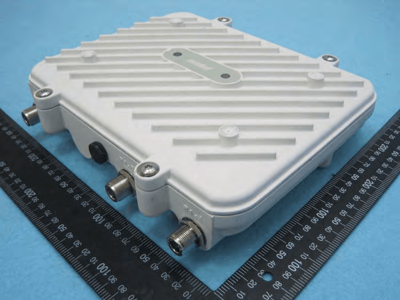
H9PAP7562
May 10, 2015802.11 abgn/ac Access Point
Equipment Class
DTS - Digital Transmission System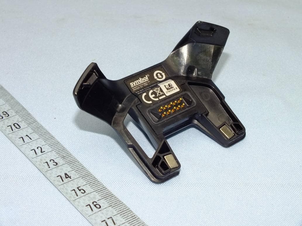
H9PTC75AH
Mar 26, 2015Touch Computer
Equipment Class
NII - Unlicensed National Information Infrastructure TX
H9PRA1202
Sep 24, 2014UHF Narrowband Radio Module
Equipment Class
TNB - Licensed Non-Broadcast Station Transmitter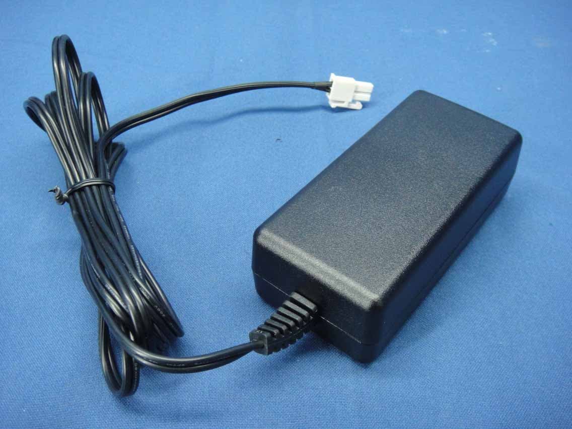
H9PEMG101
Aug 26, 2014802.15.4 Gateway
Equipment Class
DTS - Digital Transmission System