I2OMCPA4080PCS Multicarrier Ultra-Linear Power Amplifier
Powerwave Technologies, Inc.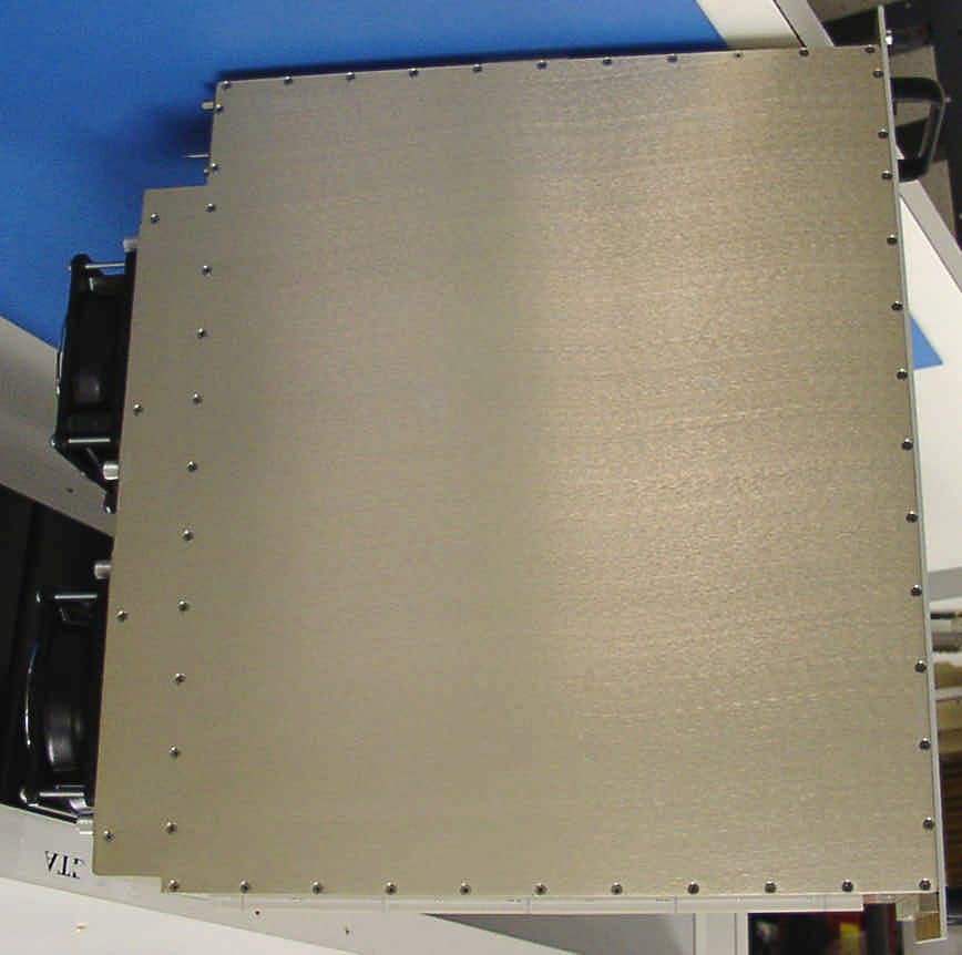
Click to zoom
Application Details
- Equipment Class
- AMP - Amplifier
- Date of Grant
- Dec 05, 2001
- Application Purpose
- Original Equipment
- Date of Application
- Dec 05, 2001
- Equipment Note
- PCS Multicarrier Ultra-Linear Power Amplifier
- Frequency Range
- 1930.00000000 - 1990.00000000
- Company
- Powerwave Technologies, Inc.
- Country
- United States
Documents & Files
Document Text
Text extracted from the exhibit documents filed with the FCC. Open a document above to read the original.
Users Manual
SPECTRIAN MCPS4080 SERIES MCPA MultiCarrier Amplifier Systems INSTALLATION & OPERATION MANUAL December 2001 Rev 1.5 Introduction iiMCPS4080 Operations Manual 2001 Spectrian Corporation. All rights reserved. 2001 Spectrian Corporation. This document co ntains proprietary information of Spectrian Corporation . No part of this manual may be copied or disclosed witho ut written authorizatio n of Spectrian Corporation. All rights reserved. Introduction MCPS4080 System Operationiii 2001 Spectrian Corporation. All rights reserved. TABLE OF CONTENTS 1Introduction .................................................................................................................................... 1 1.1About this Manual................................................................................................................... 1 1.2Safety Information................................................................................................................... 2 1.3Introduction to the MCPS4080 Family ................................................................................... 3 1.3.1MCPA Module Functional Description .......................................................................... 4 1.3.2MCPS4080 Amplifier System......................................................................................... 5 2Planning and Preparation................................................................................................................. 7 2.1Installation Planning................................................................................................................ 7 2.2Site Planning Guide................................................................................................................. 7 2.2.1Site Considerations.......................................................................................................... 7 2.2.2Rack Installation Considerations..................................................................................... 8 2.2.3Cable Connections........................................................................................................... 9 2.3Determine the required RF input power................................................................................ 10 2.3.1Set RF input drive power for each channel ................................................................... 11 2.4Prepare for Installation .......................................................................................................... 12 2.4.1Inventory Received Equipment..................................................................................... 12 2.4.2Unpack Received Equipment ........................................................................................ 12 2.4.3Repackaging for Return Shipment ................................................................................ 13 3MCPS4080 Installation ................................................................................................................. 14 3.1Introduction ........................................................................................................................... 14 3.2Task safety equipment, tools and materials .......................................................................... 14 3.3Rack Installation.................................................................................................................... 15 3.3.1Install Shelf Subassembly ............................................................................................. 15 3.3.2Install Modules in Shelf ................................................................................................ 16 3.4Cable and Wire Connections................................................................................................. 16 3.4.1Connect Chassis Ground Wire ...................................................................................... 16 3.4.2Connect DC Input Power Cables .................................................................................. 16 3.4.3Connect RF Output and Input Cables ........................................................................... 17 3.4.4Connect Alarm Interface Cables ................................................................................... 18 3.5Finish Installation.................................................................................................................. 18 3.5.1Set the MCPS4080 unit address .................................................................................... 18 3.5.2Verify Installation.......................................................................................................... 18 4System Start-Up ............................................................................................................................ 19 4.1Introduction ........................................................................................................................... 19 4.2Safety Information and Tools................................................................................................19 4.3Verify system installation...................................................................................................... 19 Introduction ivMCPS4080 Operations Manual 2001 Spectrian Corporation. All rights reserved. 4.4Power Up the MCPS4080......................................................................................................20 5MCPS4080 System Monitoring.....................................................................................................21 5.1Introduction............................................................................................................................21 5.2Monitoring the MCPS4080 System Operation......................................................................21 5.3Alarm Definitions ....................................................................................…
Text truncated - open the document above for the full version.
Cover Letter(s)
(November 14, 2001) Federal Communications Commission Authorization and Evaluation Division 7435 Oakland Mills Road Columbia, MD 21046 Re: Request for Confidentiality In reference to the application under FCC ID: (I20MCPA4080), and pursuant to Sections 0.457(d)(1)(ii) and 0.459 of the Commission's Rules, the Applicant hereby requests confidential treatment of the accompanying information as outlined below: Schematics Bill of Material of 02-000174-7 Block Diagram Function of Active Circuit Components Rationale for request for confidentiality: Spectrian has invested considerable time and materials in research and development to produce the referenced product. Disclosure of the confidential portions of this application to competitors would give them competitive advantage in developing similar products. The Applicant understands that pursuant to Rule 0.457(d)(1)(ii), disclosure of this Application and all accompanying documentation will not be made before the date of the Grant for this application. Sincerely, (Charles S Robertson III) Executive Director of Engineering) (Telephone) (408) 745-5507 (Fax) (408) 541-0265 (E-mail) [email protected] Spectrian 350 West Java Drive Sunnyvale, CA 94089
Parts List/Tune Up Info
PCS MCPA Top Level Alignment Procedure Page 1 of 12 PCS MCPA Top Level Amplifier Alignment Procedure (Version 1.7) December 6, 2001 Rev 1.7 PCS MCPA Top Level Alignment Procedure Page 2 of 12 1 Purpose: The intent of this document is to describe the specifics of a method to tune and align the PCS MCPA Power Amplifier. This procedure is based upon the Universal Method proposed by Steve Avis. At the beginning of the procedure the operator (engineer, technician or otherwise) will have an un-tuned, complete assembly. If the unit successfully passes through the procedure the assembly will be a fully tuned and functional unit. 2 Outline: This document is divided into 4 major sections to show below. The document will elaborate on each step, giving step-by-step instructions for all portions of the procedure. PROCESS STEPS: I. Prep Check connections and quality of assembly Set default settings for each of the loops II. Network Analyzer Measurements Small signal alignment of Loop1 Small signal alignment of loop2 III. Spectrum Analyzer Measurements Verification of proper Loop1 Carrier Cancellation Verification of proper Loop2 performance/targets IV. Detector Calibration and Alarm settings 3 Procedure 3.1 Prep 3.1.1 Inspection Inspect all RF and DC connections for proper installation. [Refer to the AI-02-000174] Make sure all DC connections are present and firmly plugged in. Make sure all RF cables are installed and firmly plugged in. 3.1.2 Setting Defaults A. Start the GUI B. Attach the cable adapter to the RF/DC connector on the PA. Affix with 4 screws to secure the connection. C. Disconnect RF in from the unit, at the input to the preamp. PCS MCPA Top Level Alignment Procedure Page 3 of 12 D. Set Power Supply to +27V. When brought up, the unit should have about 19.3A of current. (18.6 - 21.5 A spec range) E. Measure the voltage at points and insure the voltage is 27±.1 Vdc F. On the GUI Hit “Cal DC” The DC input should read 26.97V on the GUI. G. Hit “Disable” on the GUI (Note: The fans will turn off when this is done). Unit should be drawing 0.9-1.1A H. Open the “Loop1” window and with Loop1 disabled, and Manual control set to ON, set the DAC Sliders On Loop1 to the following setting: Slider NameSlider Value PA275 PP512 L1A2210 L1P3512 L1A190 L1P1120 Measure voltage between these 2 points Disconnect input cable here. PCS MCPA Top Level Alignment Procedure Page 4 of 12 L1P2120 L1P4“ON” Insert a picture of the GUI 1. Click on <Save to Flash> 2. Click on <Revert> 3. Click on <Manual Control> OFF then <Manual Control> ON to make sure the values got stores. 4. Hit quit and go back to main GUI screen when done. I. Open the “Loop2B” window, 1. make sure Loop2 is disabled, 2. manual control is ON and 3. set the DAC Sliders On Loop2 to the following settings: Slider NameSlider Value L2A2210 L2P3512 L2A190 L2P2120 L2P1120 L2P4“ON” Insert a picture of the GUI 4. Click on <Revert> 5. Click on <Manual Control> OFF then <Manual Control> ON to make sure the values got stores. 6. Hit quit and go back to main GUI screen when done. Finished with Initial Setup – Go to next section! 3.2 Network Analyzer Measurements 3.2.1 Loop 1 Carrier Cancellation Alignment Steps 1. From the Main GUI enable the amplifier 2. Select the Loop 1 GUI 3. In the lower left hand corner of the GUI are the Main amp and Error amp controls. Select off for these amplifiers and click on <Change>. Current should be 6.3-7.2A (6.9A typ). 4. Select <Disable> for the loop. 5. Recall “Loop1” calibration on network analyzer – the calibration should be from 1910MHz to 2010MHz. Note that the measurement bandwidth is 1930-1990MHz in this case. 6. Connect the VNA port 1 to the input to the preamp (if applicable) and port 2 to the output of the carrier cancellation board. (insert a photo here) 7. Disconnect the main path sample cable from J9 and terminate that port in 50 ohms. 8. Go into the manual mode (Manual mode ON) PCS MCPA Top Level Alignment Procedure Page 5 of 12 9. Measure the reference delay path from 1930-1990MHz. Use split screen display on VNA to measure gain and phase at the same time. Set Marker 1 to 1930MHz, Marker 2 to 1960MHz, Marker 3 to 1990MHz. Phase, Channel 1, scale=2°/div, buttons sequence. a) Make Marker 2 active (1960MHz) b) Press <Marker Function>, <Marker to delay>, <Marker to reference> c) <Scale>, <Electrical delay> d) Adjust delay for flattest phase response 1930-1990MHz (scale 2°/div), <Marker to reference> e) Peak to peak flatness should be less than 2 degrees, if it is more than 2 degrees, then there is something wrong with the reference path – move the unit to the troubleshooting area and mark the test as FAIL and indicate REFERENCE PATH PHASE FLATNESS OUT OF SPEC. f) <Display>, <Data to Memory>, <Data – Memory> g) <Scale>, <phase offset>, on the keypad put in 180 and hit the <x> button. Gain, Channel 2, scale=.2dB/div, buttons sequence. a) <scale>, <marker to reference> b) Using R279 adjust the loop 2 gain slope adjuster for optimum flatness. c) Repeat step a). ** Peak to peak flatness should be less than 1.0dB, if it is more than 1.0dB, then there is something wrong with the reference path – move the unit to the troubleshooting area and mark the test as FAIL and indicate REFERENCE PATH AMPLITUDE FLATNESS OUT OF SPEC. Disconnect this cable (J1) and insert test cable from port 1 of the vector Network Analyzer Disconnect this cable (J10) and insert test cable from port 2 of the vector Network Anal yzer PCS MCPA Top Level Alignment Procedure Page 6 of 12 <Display>, <Data to Memory>, <Data – Memory> 10. Reconnect the main path sample cable to the carrier cancellation board. 11. Enable main amplifier (Loop1 -> Main Amp ON, Error Amp OFF) 12. Using manual gain slider (L1A1) adjust gain to reference value. Use the Loop1 slope adjustment (R34) if necessary to match gain flatness with reference path. This must be done prior to adjusting the phase as it can modify the delay. Main Path should have a flatness of less than 1.0dB peak…
Text truncated - open the document above for the full version.
Test Report
FCC CFR47 PART 24 E CERTIFICATION TEST REPORT FOR PCS MULTI CARRIER POWER AMPLIFIER MODEL: MCPA4080 FCC ID: I2OMCPA4080 REPORT NUMBER: 01U1044-1 ISSUE DATE: November 12, 2001 Prepared for SPECTRIAN 350 WEST JAVA DRIVE SUNNYVALE, CA 94089 USA Prepared by COMPLIANCE ENGINEERING SERVICES, INC. 561F MONTEREY ROAD, ROUTE 2 MORGAN HILL, CA 95037, USA TEL: (408) 463-0885 FAX: (408) 463-0888 REPORT NO: 01U1044-1 DATE: NOVEMBER 12, 2001 FCC ID: I2OMCPA4080 EUT: PCS MULTI CARRIER POWER AMPLIFIER Page 2 of 102 COMPLIANCE CERTIFICATION SERVICES DOCUMENT NO: CCSUP4031A 561F MONTEREY ROAD, MORGAN HILL, CA 95037 USA TEL: (408) 463-0885 FAX: (408) 463-0888 This report shall not be reproduced except in full, without the written approval of CCS. This document may be altered or revised by Compliance Certification Services personnel only, and shall be noted in the revision section of the document. TABLE OF CONTENT 1. TEST RESULT CERTIFICATION------------------------------------------------------------------------3 2. EUT DESCRIPTION------------------------------------------------------------------------------------------4 3. TEST METHODOLOGY------------------------------------------------------------------------------------4 4. TEST FACILITY----------------------------------------------------------------------------------------------4 5. ACCREDITATION AND LISTING-----------------------------------------------------------------------4 6. MEASURING INSTRUMENT CALIBRATION--------------------------------------------------------4 7. APPLICABLE RULES AND BRIEF TEST RESULT--------------------------------------------------5 8. TEST SETUP, PROCEDURE AND RESULT-----------------------------------------------------------8 8.1. SECTION 2.1046: RF POWER OUTPUT-------------------------------------------------------------8 8.2. SECTION 2.1047: MODULATION CHARACTERISTICS-------------------------------------------9 8.3. SECTION 2.1049: OCCUPIED BANDWIDTH--------------------------------------------------------9 8.4. SECTION 2.1051: SPURIOUS EMISSION AT ANTENNA TERMINAL---------------------------12 8.5. SECTION 2.1053: FIELD STRENGTH OF SPURIOUS RADIATION----------------------------82 8.6. SECTION 2.1055: FREQUENCY STABILITY--------------------------------------------------------89 8.7. ELECTROSTATIC DISCHARGE: EN61000-4-2 -----------------------------------------------------91 ATTACHMENT----------------------------------------------------------------------------------------------------95 8.1. EUT PHOTOS--------------------------------------------------------------------------------------------95 8.2. PROPOSED FCC ID LABEL FORMAT---------------------------------------------------------------96 8.3. REQUEST FOR CONFIDENTIALITY-----------------------------------------------------------------97 8.4. USER’S MANUAL----------------------------------------------------------------------------------------98 8.5. TECHNICAL DESCRIPTION---------------------------------------------------------------------------99 8.6. THEORY OF OPERATION---------------------------------------------------------------------------100 8.7. SCHEMATIC, PART LISTS AND BLOCK DIAGRAM---------------------------------------------101 8.8. TUNE UP PROCEDURE------------------------------------------------------------------------------102 REPORT NO: 01U1044-1 DATE: NOVEMBER 12, 2001 FCC ID: I2OMCPA4080 EUT: PCS MULTI CARRIER POWER AMPLIFIER Page 3 of 102 COMPLIANCE CERTIFICATION SERVICES DOCUMENT NO: CCSUP4031A 561F MONTEREY ROAD, MORGAN HILL, CA 95037 USA TEL: (408) 463-0885 FAX: (408) 463-0888 This report shall not be reproduced except in full, without the written approval of CCS. This document may be altered or revised by Compliance Certification Services personnel only, and shall be noted in the revision section of the document. 1. TEST RESULT CERTIFICATION COMPANY NAME: SPECTRIAN 350 WEST JAVA DRIVE SUNNYVALE, CA 94089, USA CONTACT PERSON: CHARLES S ROBERTSON III / EXECUTIVE DIRECTOR OF ENGINEERING TELPHONE NO: (408) 745-5507 EUT DESCRIPTION: PCS MULTI CARRIER POWER AMPLIFIER MODEL NAME: MCPA4080 DATE TESTED: NOVEMBER 12, 2001 EQUIPMENT TYPE 1930-1990 MHz POWER AMPLIFIER MEASUREMENT PROCEDURE ANSI 63.4 / 1992, TIA/EIA 603 PROCEDURE CERTIFICATION FCC RULE CFR 47 PART 24 Subpart E Compliance Certification Services, Inc. tested the above equipment for compliance with the requirement set forth in CFR 47, PART 24 Subpart E-Broadband PCS. This said equipment in the configuration described in this report, shows the maximum emission levels emanating from equipment are within the compliance requirements. Warning : This document reports conditions under which testing was conducted and results of tests performed. This document may not be altered or revised in any way unless done so by Compliance Certification Services and all revisions are duly noted in the revisions section. Any alteration of this document not carried out by Compliance Certification Services will constitute fraud and shall nullify the document. Released For CCS By: Tested By: STEVE CHENG KERWIN CORPUZ EMC ENGINEERING MANAGER ASSOCIATE EMC ENGINEER COMPLIANCE CERTIFICATION SERVICES COMPLIANCE CERTIFICATION SERVICES REPORT NO: 01U1044-1 DATE: NOVEMBER 12, 2001 FCC ID: 120MCPA4080 EUT: PCS MULTI CARRIER POWER AMPLIFIER Page 4 of 102 COMPLIANCE CERTIFICATION SERVICES DOCUMENT NO: CCSUP4031A 561F MONTEREY ROAD, MORGAN HILL, CA 95037 USA TEL: (408) 463-0885 FAX: (408) 463-0888 This report shall not be reproduced except in full, without the written approval of CCS. This document may be altered or revised by Compliance Certification Services personnel only, and shall be noted in the revision section of the document. 2. EUT DESCRIPTION This product is designed to provide power gain over the PCS cellular band transmit frequency range of 1930 MHz to 1990 MHz, with a minimum channel frequency separation of 60 kHz and a maximum channel frequency separation of 20 MHz. 3. TEST METHODOLOGY Both conducted and radiated testing…
Text truncated - open the document above for the full version.
Test Setup Photos
REPORT NO: 01U1044-1 DATE: NOVEMBER 12, 2001 FCC ID: 120MCPA4080 EUT: PCS MULTI CARRIER POWER AMPLIFIER Page 13 of 102 COMPLIANCE CERTIFICATION SERVICES DOCUMENT NO: CCSUP4031A 561F MONTEREY ROAD, MORGAN HILL, CA 95037 USA TEL: (408) 463-0885 FAX: (408) 463-0888 This report shall not be reproduced except in full, without the written approval of CCS. This document may be altered or revised by Compliance Certification Services personnel only, and shall be noted in the revision section of the document. TEST PROCEDURE 1) Three balanced signals were applied to the RF input. One set as close as possible to the bottom of the block edge and one set as close as possible to the top of the block edge. Set the RES BW to 1% of the emission bandwidth to show compliance with the –13dBm limit, in the 1 MHz bands immediately outside and adjacent to the top and bottom edges of the frequency block. 2) For the Out-of-Band measurements a 1 MHz RES BW was used to scan from 15 MHz to 10fo of the fundamental carrier for all frequency block. A display line was placed at –13dBm to show compliance. RESULT The following table indicates the plot number associated with the Input Bandwidth, Output Bandwidth, Block Edges, Intermodulation and Out-of-Band emission plots. All measurements are in peak detector mode. REPORT NO: 01U1044-1 DATE: NOVEMBER 12, 2001 FCC ID: 120MCPA4080 EUT: PCS MULTI CARRIER POWER AMPLIFIER Page 83 of 102 COMPLIANCE CERTIFICATION SERVICES DOCUMENT NO: CCSUP4031A 561F MONTEREY ROAD, MORGAN HILL, CA 95037 USA TEL: (408) 463-0885 FAX: (408) 463-0888 This report shall not be reproduced except in full, without the written approval of CCS. This document may be altered or revised by Compliance Certification Services personnel only, and shall be noted in the revision section of the document. Fig 2: Radiated Emission – Substitution Method set-up 1 – 18 GHz Radiated Emission Setup RF Test Receiver Ant 1m 4m 0.8m 1m Ground Plane Turn Table SG Substitution Ant REPORT NO: 01U1044-1 DATE: NOVEMBER 12, 2001 FCC ID: 120MCPA4080 EUT: PCS MULTI CARRIER POWER AMPLIFIER Page 84 of 102 COMPLIANCE CERTIFICATION SERVICES DOCUMENT NO: CCSUP4031A 561F MONTEREY ROAD, MORGAN HILL, CA 95037 USA TEL: (408) 463-0885 FAX: (408) 463-0888 This report shall not be reproduced except in full, without the written approval of CCS. This document may be altered or revised by Compliance Certification Services personnel only, and shall be noted in the revision section of the document. 18 – 20 GHz Radiated Emission Setup 1 – 18 GHz Substitution Method Setup REPORT NO: 01U1044-1 DATE: NOVEMBER 12, 2001 FCC ID: 120MCPA4080 EUT: PCS MULTI CARRIER POWER AMPLIFIER Page 85 of 102 COMPLIANCE CERTIFICATION SERVICES DOCUMENT NO: CCSUP4031A 561F MONTEREY ROAD, MORGAN HILL, CA 95037 USA TEL: (408) 463-0885 FAX: (408) 463-0888 This report shall not be reproduced except in full, without the written approval of CCS. This document may be altered or revised by Compliance Certification Services personnel only, and shall be noted in the revision section of the document. 18 – 20 GHz Substitution Method Setup TEST PROCEDURE 1). On a test site, the EUT shall be placed on a turntable, and in the position closest to the normal use as declared by the user. 2). The test antenna shall be oriented initially for vertical polarization located 1m from the EUT to correspond to the frequency of the transmitter. 3). The output of the test antenna shall be connected to the measuring receiver and either a peak or average detector was used for the measurement as indicated on the report. The detector selection is based on how close the emission level was approaching the limit. 4). The transmitter shall be switched on, if possible, without the modulation and the measurement receiver shall be tuned to the frequency of the transmitter under test. 5). The test antenna shall be raised and lowered through the specified range of height until a maximum signal level is detected by the measuring receiver. 6). The transmitter shall than be rotated through 360° in the horizontal plane, until the maximum signal level is detected by the measuring receiver. 7). The test antenna shall be raised and lowered again through the specified range of height until a maximum signal level is detected by the measuring receiver. 8). The maximum signal level detected by the measuring receiver shall be noted. 9). The transmitter shall be replaced by a substitution antenna. 10). The substitution antenna shall be oriented for vertical polarization. 11). The substitution antenna shall be connected to a calibrated signal generator. 12). If necessary, the input attenuator setting of the measuring receiver shall be adjusted in order to increase the sensitivity of the measuring receiver. 13). The test antenna shall be raised and lowered through the specified range of the height to ensure that the maximum signal is received. REPORT NO: 01U1044-1 DATE: NOVEMBER 12, 2001 FCC ID: 120MCPA4080 EUT: PCS MULTI CARRIER POWER AMPLIFIER Page 92 of 102 COMPLIANCE CERTIFICATION SERVICES DOCUMENT NO: CCSUP4031A 561F MONTEREY ROAD, MORGAN HILL, CA 95037 USA TEL: (408) 463-0885 FAX: (408) 463-0888 This report shall not be reproduced except in full, without the written approval of CCS. This document may be altered or revised by Compliance Certification Services personnel only, and shall be noted in the revision section of the document. TEST SETUP ESD Test Setup Power Supply Laptop Signal Generator Coupler Combiner BP filter (part of EUT) EUT Power Meter Power Sensor BI-Directional Coupler 500W Attenuator
Contact Information
Applicant
Robert Biedka(Sr. Quality Engineer)
Test Firm
Compliance Certification Services IncSteve Cheng
Technical Specifications
| # | Rule Parts | Frequency Range | Power Output | Emission | Tolerance |
|---|---|---|---|---|---|
| 4 | 24 | 1.93 GHz - 1.99 GHz | 100 W | F9W | Amp |
Other Applications from Powerwave Technologies, Inc.
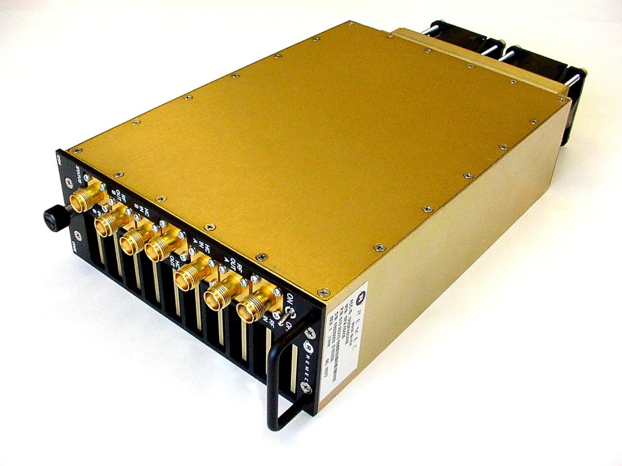
I2ODPA4040E
Jul 15, 2003PCS Dual Amplifer Booster/Combiner
Equipment Class
AMP - Amplifier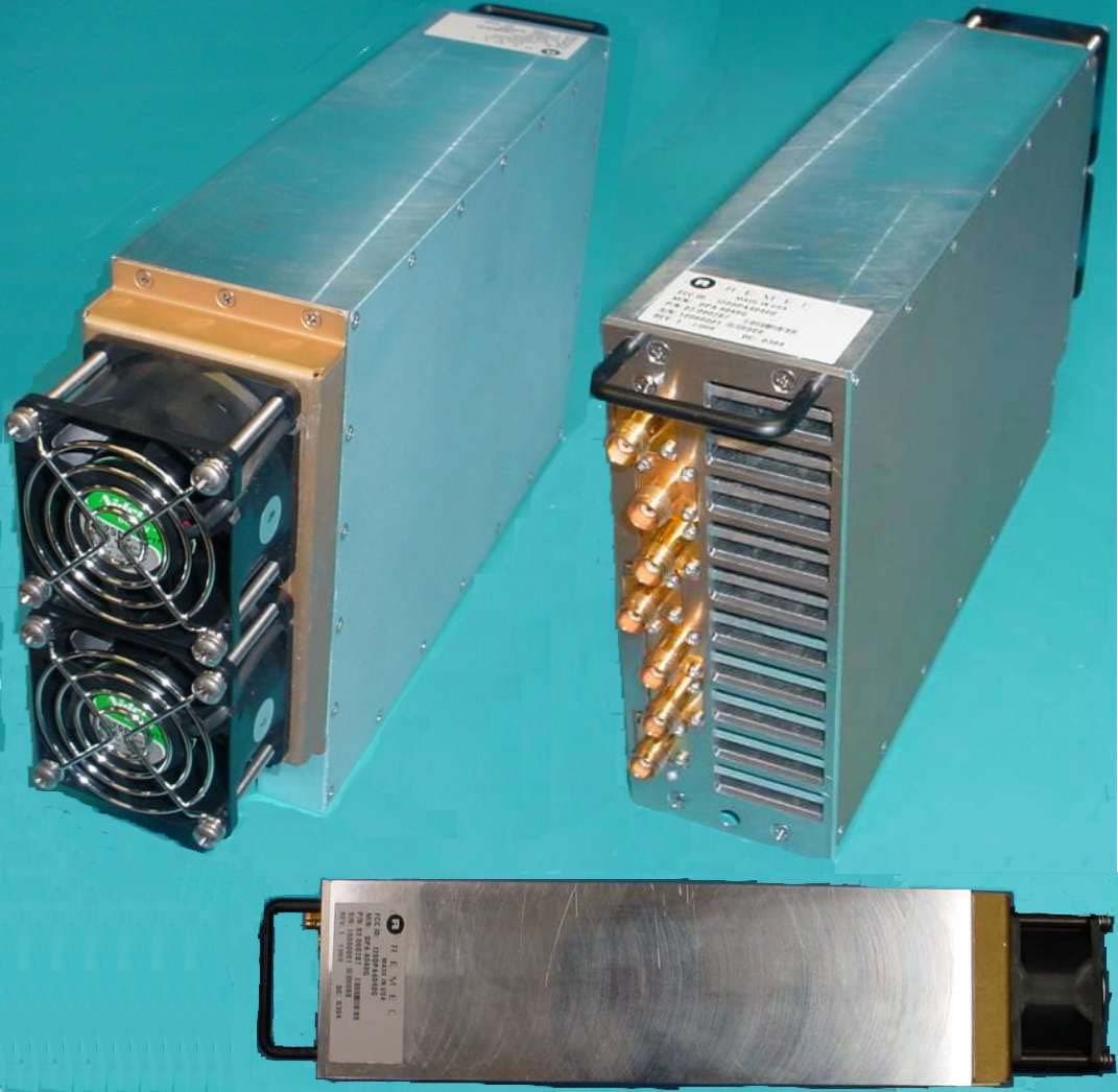
I2ODPA4040G
Mar 09, 2003PCS Dual Amplifier Booster/Combiner
Equipment Class
AMP - Amplifier
I2OMCPS2135
Aug 06, 2001MultiCarrier Amplifier System
Equipment Class
AMP - Amplifier
I2OMCPS2000
Mar 16, 1999350 Watt Multi-Carrier Power Amplifier
Equipment Class
AMP - AmplifierI2O-ORIOLE1
Feb 01, 1999Single channel PCS Base station unit
Equipment Class
AMP - Amplifier