INGIN-264TBWireless Body-Pack Transmitter
JTS PROFESSIONAL CO., LTD.
Click to zoom
Application Details
- Equipment Class
- TBC - Licensed Broadcast Station Transmitter
- Date of Grant
- Nov 05, 2012
- Application Purpose
- Original Equipment
- Date of Application
- Nov 05, 2012
- Equipment Note
- Wireless Body-Pack Transmitter
- Frequency Range
- 614.12500000 - 697.87500000
- Company
- JTS PROFESSIONAL CO., LTD.
- Country
- Taiwan
Documents & Files
Document Text
Text extracted from the exhibit documents filed with the FCC. Open a document above to read the original.
Users Manual
59508-021-02 UHF PLL Dual Channel Diversity Wireless System * The system is of the innovative design to allow changing the transmitter’s frequency by long-distance . * IN264R with band width of 36 MHz.* Preset 6 groups, maximum 23 channels in one group. 2 IN 4 6 REMOSET IN 4 2 6 R SET REMOSET SET AF RF AF RF Music Life INFINITY SET + - IN 4 2 6 TB Music INFINITY Life 01 2 IN 4 6 1. Important Caution 2. Features 3. Parts Identification 3-1 IN264R3-2 IN264TH3-3 IN264TB3-4 Accessories 4. Connection 4-1 Connect to the subsequent unit4-2 Connect the power supply unit 5. Operation 5-1 Set up the system5-2 Set up ID code5-3 Synchronize the channel5-4 Check system status5-5 Manual select channel5-6 REMOSET button lock5-7 Adjust the sensitivity of the microphone 6. Specification 01010202030404050505060606070809101113 1. Important Caution Always make all connections before plugging the unit into an AC power outlet. Do not leave the devices in a place with high temperature or high humidity.Do not handle the power cord with wet hands !Keep the devices away from fire and heat sources. Pair the ID codes of the transmitter and the receiver to have proper function. 2. Features JTS IN264 wireless microphone system is designed with the world first RF remote setting function (REMOSET). A user can set the receiver with desired frequency and press the “REMOSET” Key; then the transmitter will automatically be set. The operation distance can reach 10 meters. This brings great convenience to sound engineers during live performance. IN264 is of 36MHz bandwidth to render 23 transmitters work simultaneously. It provides great convenience to large venue. A new capsule has been developed for IN264TH . The capsule, SAM-8W, is designed for large venue with hundreds of thousands watt power. The SAM-8W delivers vivid details of vocal and instruments. The IN264 is of stylish industry design. Yet JTS bombproof quality remains as always. 2 IN 4 6 Music INFINITY Life 02 03 REMOSET IN 4 2 6 R SET REMOSET SET AF RF AF RF 3. Parts Identification 3-1 IN264R Front panel Power SwitchChannel Selector: including “ up”, “ down” and “Set” button LCD PanelREMOSET Key: press it to send a desired channel data to a transmitter Rear panel BNC antenna connectorPower Supply Jack (12-18V/600mA): for connecting the power supply unit Squelch adjuster: to adjust radio signal level of both channels Mixed AF Output (6.3mm jack, unbalanced): for connection to a balanced input, e.g. of a mixer or amplifier Balanced XLR Output: for connection to the balanced input, e.g. of a mixer or an amplifier Output Level Attenuation(-10dB,-20dB): to attenuate the balanced XLR output level by 10dB,20dB LIFT / GND 123456 768 9 1011 abc d e f g 12131415 16 17 AF RF ab d c e LCD Panel of the Receiver AF Level: display the strength of audio signal RF Level: display the strength of radio signal Antenna Status: the receiver will automatically select an antenna with stronger signal level Low battery indicator: display the low battery status of its transmitter Group & Channel: there are 6 groups, maximum 23 channels in one group. 3-2 IN264TH LCD DisplayBattery TraySet button: set the configuration of handheld transmitter Up button: select the settings of transmitter Down button: select the settings of transmitter Power and Mute Switch LCD Panel of the Handheld Transmitter Battery status: display battery status Group & Channel: there are 6 groups, maximum 23 channels in one group. 1 2 2 4 4 3 3 5 5 6 7 8 9 10 11 10 9 7 f g 1415 16 12 17 13 2 IN 4 6 Music INFINITY Life 04 05 h i 1819 20212322242625 3-3 IN264TB LCD DisplayBattery TraySet button: set the configuration of bodypack transmitter Up button: select the settings of transmitter Down button: select the settings of transmitter 4 Pin mini XLR mic. input Power SwitchGain control: control sensitivity of the transmitter Pad: -20dB, -6dB, 0dB LCD Panel of the Body-Pack Transmitter Battery status: display battery status Group & Channel: there are 6 groups, maximum 23 channels in one group. 27 3-4 Accessories AC/DC adaptorAF output cable (with Φ6.3 plug at both ends) Screwdriver (IN264TB)CM-501 (IN264TB) 27282930 27 7 9 10 4. Connection 4-1 Connect to the subsequent unit (e.g. mixer, or amplifier) Connect one end of a proper AF cable to the AF Output or Balanced XLR Output socket , then plug another end to the “MIC IN” input socket of a mixer or a amplifier (Step 1 of Figure 1) 4-2 Connect the power supply unit Plug in one end of AC/DC adaptor cable to Power Supply Jack in the rear panel of receiver, and plug another end into an AC outlet (Step 2 of Figure 1) 25 26 28 - i h 18 19 23 24 20 21 22 -20 -6 0 29 30 MIXER AUDIO OUTPUT DC INPUT Figure 1 2 1 2 IN 4 6 Music INFINITY Life 06 07 5. Operation 5-1 Set up the system A) Turn on the power of the receiver Switch the “Power Switch” to “ON”. The “LCD Panel” and “REMOSET” Key will light up.B) Turn on the power of the transmitter Press the “Power Switch” . The “LCD Display” will light up. C) Mute Function ( for IN264TH ) After the transmitter's power is on, short pressing the "Power Switch " will mute the microphone. Press the "Power Switch" again will re-activate the microphone.Notice: You have to hold the "Power Switch" for 3 seconds in order to turn off the transmitter. D) Install the antennas in a vertical position 5-2 Set up ID code In order to match one receiver channel to one transmitter, IN264 is designed with“ ID code”. If and only if both ID codes of a receiver channel and a transmitter match each other, the “REMOSET” function works. When setting the ID code, system will automatically avoid the ID code used by the other channel. There are 100 ID codes available.A) Press "Set" button for 3 seconds, LCD Panel will start flashing.B) Press "Set" to enter "ID Code" setting window. (Figure 2) C) Press " Up" or Down" button to select a distinct ID code from "id 0" to "id 99". D) After setting, press "Set" again to save the setting. 2 5 4 17 24 12 18 1 6 3 17 Receiver Handheld…
Text truncated - open the document above for the full version.
External Photos
ETC Report No.:11-07-RBF-190 Sheet 1 of 7 Sheets FCC ID.:INGIN-264TB Rev. 2.0 CONSTRUCTED PHOTOS of EUT 1. Top View of EUT 2. Side View of EUT ETC Report No.:11-07-RBF-190 Sheet 2 of 7 Sheets FCC ID.:INGIN-264TB Rev. 2.0 CONSTRUCTED PHOTOS of EUT 3. Side View of EUT 4. Front View of EUT ETC Report No.:11-07-RBF-190 Sheet 3 of 7 Sheets FCC ID.:INGIN-264TB Rev. 2.0 CONSTRUCTED PHOTOS of EUT 5. Front View of EUT 6. Bottom View of EUT
ID Label/Location Info
FCC ID label location Label here 得琦電子股份有限公司 TEL: 04-24938803 FAX: 04-24914890 MO-- 完成日發稿日再完稿再完稿 董事長副總營業研發設計 材質發稿方式尺寸顏色 廠商: Date: 料號: From: 品名: 註 解 成品 鈺婷 2012 05 18 20120522 e-mail E-mail: [email protected]分機550 其它標籤 印FCC ID :INGIN-264TB 52884-010 RD 25*6mm灰底白字反銀龍紙 FCC ID: INGIN-264TB
Internal Photos
ETC Report No.:11-07-RBF-190 Sheet 5 of 7 Sheets FCC ID.:INGIN-264TB Rev. 2.0 CONSTRUCTED PHOTOS of EUT 8. Internal View of EUT ETC Report No.:11-07-RBF-190 Sheet 6 of 7 Sheets FCC ID.:INGIN-264TB Rev. 2.0 CONSTRUCTED PHOTOS of EUT 9. Solder View of PCB 10. Component View of PCB ETC Report No.:11-07-RBF-190 Sheet 7 of 7 Sheets FCC ID.:INGIN-264TB Rev. 2.0 CONSTRUCTED PHOTOS of EUT 11. Solder View of PCB 12. Component View of PCB
Schematics
1 2 3 4 5 6 78 ABCD 8 7 6 5 4 3 2 1 D CBA R9390 R104.7K C1633N R1833K C221N R1610K C21100P R1222K R1322K + C2010uF/16V + C1210uF + C410uF C727P VR210K R2810K AF-OUT + C2310uF R3568K R3610K C2510P C29470N R421K R43100K R2110K R2210K + C1510uF C2422P + C3410uF +R5V R3815K C2722N C3610N 1 2 3 4 56 7 8 9 10 U3NJM2761 + C4110uF C19100N C26100P R2510K C31N C3110N C81N R851K R3510K 234 1 SW1SW 1P3T R1 R171M C171N R1510K R1422K 1234 CON1 MH1-41-043N R1122K R191K + C3310uF R3094.7K Q305DTC144EE AFC ToneCtrl C307470N R30815K C3081N R302100 + C31010uF Q303 DTC144EE 1234 CON2 21 3 U2ASA575 1819 17 U2CSA575 161511 20 12 8 10 13 14 U2DSA575 C5100N C6100N R42.2K R582K 23 1 8 U1A2115 65 7 4 U1B2115 C22.2uF C11uF R304100K R303100K R305100K C303120P C3024.7P C3041N C306330P C305220P X30132.768KHz R3071M R306100K R27 43 1 25 U301MCP6291 284 5167 3 U47411 C3712P C38100N R6 Q2AUMX18N Q1A UMX18N Q1BUMX18N Q2BUMX18N Sen0Sen1Sen2 Sen0 Sen1Sen2 C11100P R253.9K C1410uF C3210uF C3510uF C301uF C1310uF R3410K R3710K C181uF VDD 8 CS 1 SCK 2 SDI 3 VSS 4 PA0 5 PW0 6 PB0 7 U6MCP4151 Q301AUMX1N Q301BUMX1N 3 2 VR1100K 1 2 3 4 5 6 78 ABCD 8 7 6 5 4 3 2 1 D CBA R1064.7K R107220 R1081K + C1101uF + C1130.1uF C114100P L101100N SVC1T8 C119100P L1055.6nH C1200.5P C12212P + C11122uF X1014MHz VC10120P C10647P C1051N + C14110uF C13922N R113100K R10110KR10210KR10310K C102100P C103100P R114 10K C101100P + C13810uF C14022N L104100N P_3V SVC2T8 C1210.5P C13010N C129100P C117100P C115180P R1112.2K R1102.7K C10910N L103100N C131100N R121100K + C13410uF C209100P C205100P Q202P1 Q201 P5 C13622P R2053.9K AF-OUT VC10210P C143100N + C14210uF + C14522uF C2171N C144100N C2181N C2201N +R4V R10910K C146100N R10522 + C10710uF C108100N +R5V C2081N C2191N ANT201 ANT C2155.6P C2135.6P M1EMI C2115.6P L20810N L20710N C210100P L20610N C2031P C22210N R20922 C22110N C206100P L205100N R2071.5K C20712P L2042.2N R20310 R202100 R208560 C2041N L202100nH R2132.2K R2042.7K C2022.7P L20112nH R2061K C216100P L20322N OSCin 1 OSCout 2 Vp 3 Vcc 4 Do 5 GND 6 Xfin 7 fin 8 Clock 9 Data 10 LE 11 PS 12 ZC 13 LD/fout 14 @P 15 @R 16 U101MB15E03SL 1 5 2 3 4 U103TC1014-4.0 L10712nH C133100P RFCPLL_SCKPLL_SDAPLL_LE 2 1 3 U102MCP1700-3.0 AFCToneCtrl C1231.5P R20110 C126 1N C1243.3P Q10224 C1252.2P R1173.3K R118330 R1202.7K R1165.6K R122390 L10210nH R1155.6K C1275.6P Q10124 C1324.7P R125 + C12822uF + C14747uF C1354.7P C148100P C149100N Q204P6002CYG Q203P6002CYG R21510 R214390 R216100K L106L Q209DTC144EE R223100K R22010K Q207AUMF5N Q208AUMF5N Q207BUMF5N Q208BUMF5N R221100K R2224.7K R218100K R21910K 1 2 3 4 U201XC8102 1 2 3 4 5 6 7 8 9 10 11 12 13 14 15 16 17 18 19 20 CON101CPB7220-12 PLUG Sen0Sen2Sen1 1 5 2 3 4 U104TK70008S C1374.7uF D1011SS400 R123390K R1240 C1182.2uF C2121P C2141P R217 1 2 3 4 5 6 78 ABCD 8 7 6 5 4 3 2 1 D CBA Title Number Revision Size A3 Date: 27-Sep-2010 Sheet of File: C:\Documents and Settings\All Users\Documents\MyDesign1\MyDesign1.ddb Drawn By: VSS 41 VSS 56 AVSS 25 VSS 9 RD6/SEG19 1 RD7/SEG20 2 RF0/SEG32 11 RF1/SEG33 12 RF2/SEG34 13 RF3/SEG35 14 RG0/SEG36 3 RG1/SEG37 4 RG2/SEG38 5 RG3/SEG39 6 RG4/SEG40 7 VDD 10 AVDD 26 VDD 38 VDD 57 VDD 19 VSS 20 RA7/OSC1/T1OSI 39 RA6/OSC2/T1OSO 40 RG5/SEG41 8 RB0/INT/SEG0 15 RB1/SEG1 16 RB2/SEG2 17 RB3/SEG3 18 RB4/COM0 21 RB5/COM1 22 RB6/SEG14 23 RB7/SEG13 24 RA0/AN0/SEG12 27 RA1/AN1/SEG7 28 RA2/AN2/COM2 29 RA3/AN3/SEG15 30 RA4/AN4/SEG4 31 RA5/AN5/SEG5 32 RE0/AN5/SEG21 33 RE1/AN6/SEG22 34 RE2/AN7/SEG23 35 RE3/MCLR 36 RE4/SEG24 37 RE5/SEG25 42 RE6/SEG26 43 RE7/SEG27 44 RF4/SEG28 45 RF5/SEG29 46 RF6/SEG30 47 RF7/SEG31 48 RC0/VLCD1 49 RC1/VLCD2 50 RC2/VLCD3 51 RC3/SEG6 52 RD0/COM3 53 RD1 54 RD2/CCP2 55 RD3/SEG16 58 RC4/T1G/SDO/SEG11 59 RC5/T1CKI/SEG10 60 RC6/TX/SCL/SEG9 61 RC7/RX/SDA/SEG8 62 RD4/SEG17 63 RD5/SEG18 64 U503PIC16F946 COM1 15 COM2 14 COM3 13 SEG1 11 SEG2 10 SEG3 9 SEG4 8 SEG5 7 SEG6 6 SEG7 5 SEG8 4 SEG9 3 SEG10 2 SEG11 1 SEG12 22 SEG13 21 SEG14 20 SEG15 19 SEG16 18 COM4 12 SEG17 17 SEG18 16 LCD501LCD950 R53147K R53247K +M3V SW502SETSW504DownSW503Up R53047K KeySetKeyUpKeyDN COM0COM1 COM2 PGCPGDVLCD1VLCD2VLCD3 SEG00SEG01SEG02SEG03SEG04SEG05SEG06SEG07SEG08SEG09SEG10SEG11SEG12SEG13SEG14SEG15SEG16SEG17 seg00seg01seg02seg03seg04seg05seg06seg07seg08seg09seg10seg11seg12seg13seg14seg15seg16seg17BLCRmLEDRmEN COM0COM1COM2COM3 RmSDRmSK PWCSwInBattIn COM3 C514100N C513100N C512100N C511100N C510100N C517100N C516100N C515100N VLCD1VLCD2VLCD3 R51410KR51510KR51610K +5V SDA 5 SCL 6 WP 7 VCC 8 A0 1 A1 2 A2 3 GND 4 U50424LC16B/SN R5284.7K R5274.7K MCLRSCLSDA +M3V PGCPGD MCLR C508100N R51210K C507100NR5291K R52651 C506100N Q501DTC124XE R524100K SwIn R51833K D501RB520 R501100K D502RB520 R517100K R51933K C50422N + C50210uF C50322N BattIn D503RB520 + C5091uF D504RB520 R52222K Batt +M3V +5V +5V +M3V D505RB520 + C50110uF PWCo PWC LED502LEDLED503LED R511100 BLC LED501LED R503100 RmLED C505100N +5V Q503DTC124XE +5V R51310K SW501NSS502 SDA 1 SCL 2 MCLR 3 VDD 4 GND 5 PGD 6 PGC 7 CON501ICSP & I2C +M3V RFCoPeakiPSKoPSDoPLEo AFCoToneCo +5V R504 100 R505 100 R506 100 R507 100 R508 100 R509 100 R510 100 PeakPSDPSKPLERFC AFCTC AFCTC PeakPSD PSK PLE RFC KeyUP KeyDN KeySetSCLSDAMCLR Batt+PWCo 2 1 3 U501 MCP1700-3.0 R502100 Batt+ RmRES RmSCKRmSDA RmEN RmRES RmENRmSDRmSKRmRES JP1 R533100K Batt+ Batt- Q601P5002CMG +5V R605 + C60122uF C60210uF RFH/L RFH/L 43 1 25 U502MCP6001 C606 10uF L60110uH C60412P R60218KR603180K L60210uH + C60847uF + C60722uF C60310uF 12345 6789 10 U601XC9128 1 2 3 4 U602XC8102 + C60947uF +5V 1 2 3 4 5 6 7 8 9 10 11 12 13 14 15 16 17 18 19 20 CON502HEADER 10X2 Sen0Sen1Sen2 Sen2Sen0Sen1 LED504LED Q502DTC124XE 3 1 2 4 5 U602-1 1 2 3 4 56 ABCD 6 5 4 3 2 1 D CBA Batt+ SCLK 1 SO/GDO1 2 GDO2 3 DVDD 4 DCOUPL 5 GDO0 6 CSn 7 Xosc1 8 AVDD 9 Xosc2 10 AVDD 11 RF_P 12 RF_N 13 AVDD 14 AVDD 15 GND 16 RBIAS 17 DGOARD 18 GND 19 SI 20 U703CC2500 C716100P C715100P C7171P L7021.2N C7181P L7011.2N C7191.8P L7031.2N C7201.5P R70856K C709100N C708100N X70126MHz C710100N C711100N C72122P C72222P TEST 22 VCC 23 P2.5 24 VSS 2 P2.7 3 P2.6 4 RST 5 P2.0 6 …
Text truncated - open the document above for the full version.
Test Report
Rev. 2.0 FCC Part 74 Subpart H EMI TEST REPORT of E.U.T. : Wireless Body-Pack Transmitter FCC ID. : INGIN-264TB Model No. : IN-264TB Working Frequency: 502~607.875, 614.125~697.875 MHz for APPLICANT : JTS Professional Co., Ltd. ADDRESS : No. 148, Industry 9th Road, Tali Dist., Taichung City 41280, Taiwan, R.O.C. Test Performed by ELECTRONICS TESTING CENTER (ETC) , TAIWAN NO. 34. LIN 5. DINGFU, LINKOU DIST., NEW TAIPEI CITY, TAIWAN, 24442, R.O.C. TEL : (02)26023052 FAX : (02)26010910 http:// www.etc.org.tw ; e-mail:[email protected] Report Number : 11-07-RBF-190 ETC Report No.:11-07-RBF-190 FCC ID.:INGIN-264TB Rev. 2.0 TEST REPORT CERTIFICATION Applicant : JTS Professional Co., Ltd. No. 148, Industry 9 th Road, Tali Dist., Taichung City 41280 Taiwan, R.O.C. Manufacturer : JTS Professional Co., Ltd. No. 148, Industry 9 th Road, Tali Dist., Taichung City 41280 Taiwan, R.O.C. Description of EUT : a) Type of EUT : Wireless Body-Pack Transmitter b) Trade Name : JTS c) Model No. : IN-264TB d) FCC ID : INGIN-264TB e) Working Frequency : 502~607.875, 614.125~697.875 MHz f) Power Supply : DC 1.5V Battery*2 Regulation Applied : FCC Rules and Regulations Part 74 Subpart H I HEREBY CERTIFY THAT; The data shown in this report were made in accordance with the procedures given in ANSI C63.4 and the energy emitted by the device was founded to be within the limits applicable. I assume full responsibility for accuracy and completeness of these data. ETC Report No.:11-07-RBF-190 FCC ID.:INGIN-264TB Rev. 2.0 Issued Date : Oct. 18, 2012 Test Engineer : ( Vincent Chang, Engineer ) Approve & Authorized Signer : S. S. Liou, Section Manager EMC Dept. II of ELECTRONICS TESTING CENTER, TAIWAN ETC Report No.:11-07-RBF-190 FCC ID.:INGIN-264TB Rev. 2.0 Table of Contents Page 1. GENERAL INFORMATION ............................................................................................................................... 1 1.1 PRODUCT DESCRIPTION........................................................................................................................................... 1 1.2 TEST METHODOLOGY.............................................................................................................................................. 1 1.3 TEST FACILITY........................................................................................................................................................ 1 2. REQUIREMENTS OF PROVISIONS ................................................................................................................ 2 2.1 DEFINITION............................................................................................................................................................. 2 2.2 FREQUENCIES AVAILABLE...................................................................................................................................... 2 2.3 REQUIREMENTS FOR RADIO EQUIPMENT ON CERTIFICATION.................................................................................. 2 2.4 LABELING REQUIREMENT........................................................................................................................................ 3 3. OUTPUT POWER MEASUREMENT ................................................................................................................ 4 3.1 PROVISION APPLICABLE.......................................................................................................................................... 4 3.2 MEASUREMENT PROCEDURE................................................................................................................................... 4 3.3 TEST DATA.............................................................................................................................................................. 6 3.4 RESULT CALCULATION............................................................................................................................................ 7 3.5 TEST EQUIPMENT.................................................................................................................................................... 7 4. MODULATION CHARACTERISTICS ............................................................................................................. 8 4.1 PROVISIONS APPLICABLE........................................................................................................................................ 8 4.2 MEASUREMENT METHOD........................................................................................................................................ 8 4.3 MEASUREMENT INSTRUMENT.................................................................................................................................. 9 4.4 MEASUREMENT RESULT.......................................................................................................................................... 9 5. OCCUPIED BANDWIDTH OF EMISSION .................................................................................................... 11 5.1 PROVISIONS APPLICABLE...................................................................................................................................... 11 5.2 MEASUREMENT METHOD...................................................................................................................................... 11 5.3 OCCUPIED BANDWIDTH TEST EQUIPMENT............................................................................................................ 11 5.4 BANDWIDTH MEASURED....................................................................................................................................... 12 5.4.1 Input Level Derived...................................................................................................................................... 12 5.4.2 Occupied Bandwidth Plotted.............................................................…
Text truncated - open the document above for the full version.
Test Setup Photos
ETC Report No.:11-07-RBF-190 Sheet 32 of 40 Sheets FCC ID.:INGIN-264TB Rev. 2.0 6.6 Radiated Measurement Photos
Contact Information
Applicant
Chao-Wei Chung(General Manager)
Test Firm
Taiwan Testing and Certification CenterAnderson Ku
Technical Specifications
| # | Rule Parts | Frequency Range | Power Output | Emission | Tolerance |
|---|---|---|---|---|---|
| 2 | 74 | 614.125 MHz - 697.875 MHz | 8.70 mW | 83K4F3E | 0.005 % |
Other Applications from JTS PROFESSIONAL CO., LTD.

INGSIEM-121T
Dec 01, 2024In-Ear Monitoring System
Equipment Class
DWM - Part 15 Wireless Microphone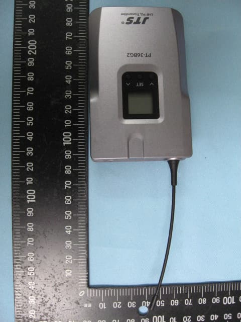
INGPT36BG2
Dec 02, 2014UHF PLL Body-Pack Transmitter
Equipment Class
TBT - Licensed Broadcast Transmitter Worn on Body
INGUF-10TH
May 06, 2013UHF PLL Handheld Transmitter
Equipment Class
TBC - Licensed Broadcast Station Transmitter
INGTG-64T
Mar 13, 2013Wireless Tour Guide Transmitter
Equipment Class
TBT - Licensed Broadcast Transmitter Worn on Body
INGMH-35
Oct 24, 2012UHF PLL Handheld Transmitter
Equipment Class
TBC - Licensed Broadcast Station Transmitter