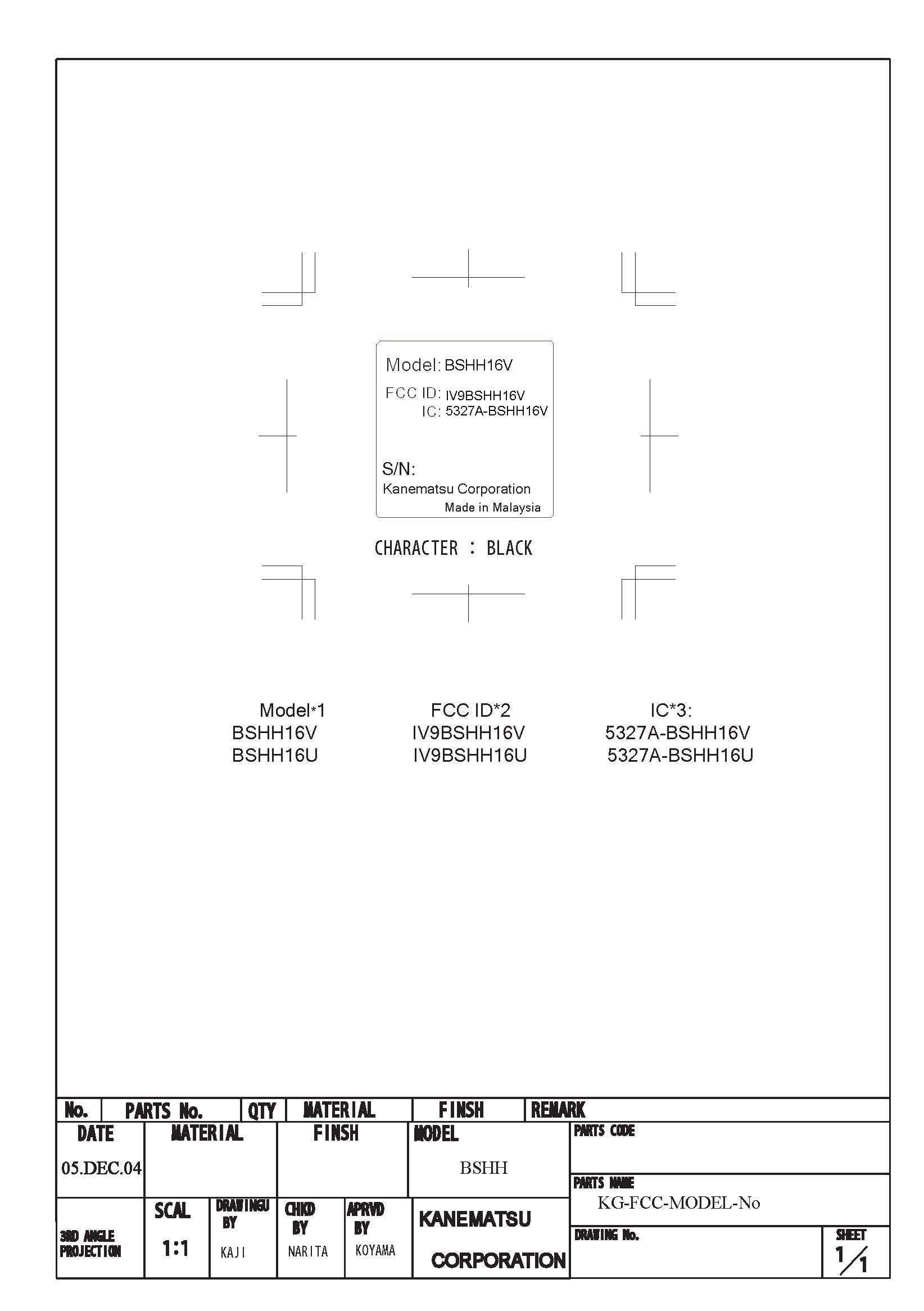
IV9BSHH16VVHF Transceiver
Kanematsu USA Inc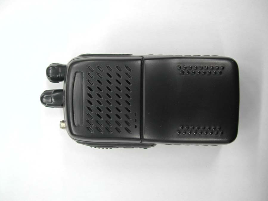
Click to zoom
Application Details
- Equipment Class
- TNF - Licensed Non-Broadcast Transmitter Held to Face
- Date of Grant
- Dec 30, 2004
- Application Purpose
- Original Equipment
- Date of Application
- Dec 30, 2004
- Equipment Note
- VHF Transceiver
- Frequency Range
- 136.00000000 - 174.00000000
- Company
- Kanematsu USA Inc
- Country
- United States
Documents & Files
Document Text
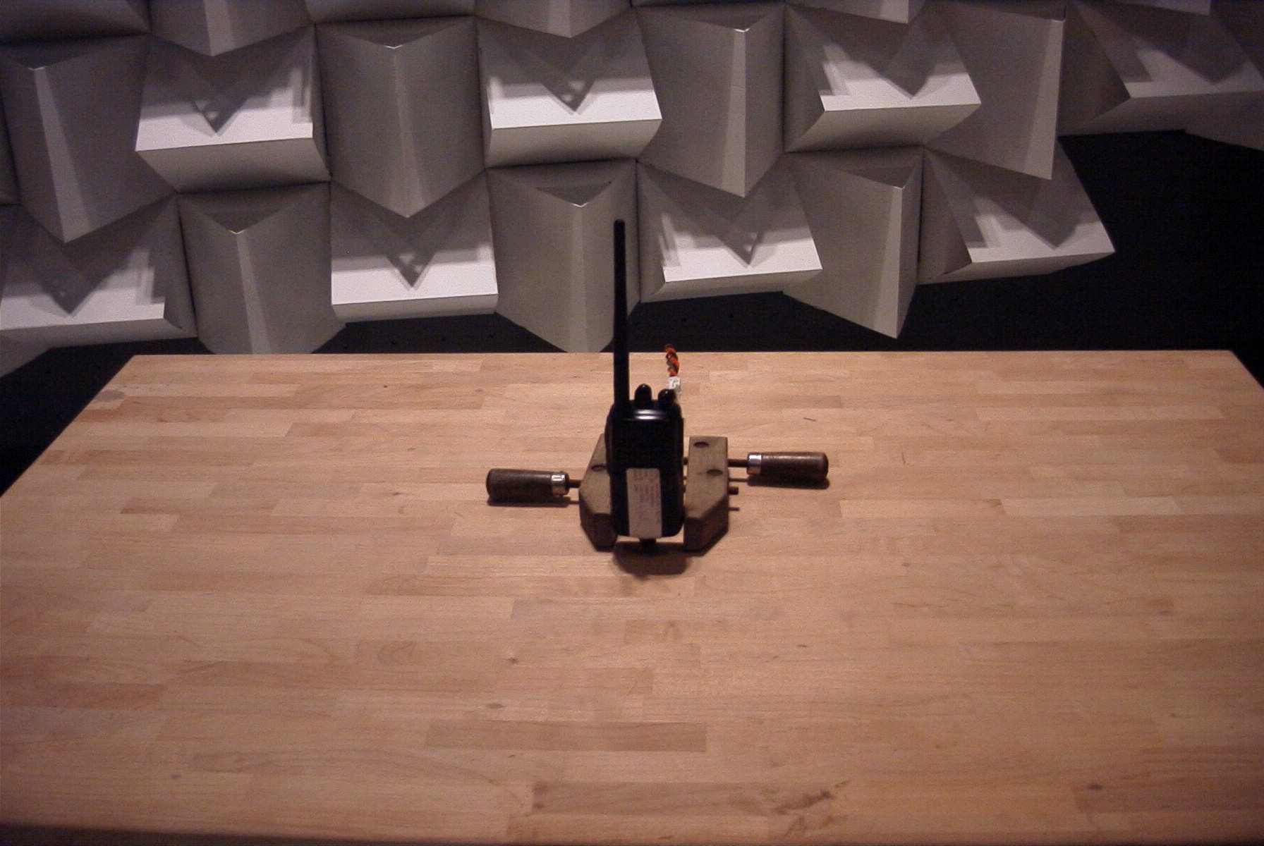
Text extracted from the exhibit documents filed with the FCC. Open a document above to read the original.
Users Manual
BS HH1 6 Users Manual INTRODUCTION This Manual describes the operation for the Kanematsu Handheld radio This Handheld is full-featured FM transceiver designed for flexible mobile business communications in the VHF or UHF Land mobile bands. This Land mobile radio can be programmed with 16 channels. Important channel frequency data is stored in EEPROM and flash memory on the CPU, and easily programmable by dealers using personal computer and PC EDITER software. FCC Requirements Your radio must be properly licensed Federal Communications Commission prior to use. Your Wireless dealer can assist you in meeting these requirements. Your dealer will program each radio with your authorized frequencies, signaling codes, etc., and will be there to meet your communications needs as your system expands. This device complies with part 15 of the FCC Rules. Operation is subject to the Condition that this devices does not cause harmful interference . NOTE: The manufacturer is not responsible for any radio or TV interference caused by unauthorized modifications to this equipment. Such modifications could void the user's authority to operate the equipment. SAFETY WARNING INFORMATION READ THIS IMPORTANT INFORMATION ON SAFE AND EFFICIENT OPERATION BEFORE USING YOUR LAND MOBILE RADIO Only qualified technicians are allowed to repair this product. Do not operate the radio without a proper antenna attached. As this may damage the radio and may also cause to exceed FCC RF exposure limits. Typical electronic systems that may malfunction due to the lack of protection from radio frequency energy present when transmitting. If the vehicle contains such equipment, consult the dealer. Just as it is dangerous to fuel a vehicle with motor running, similar hazard exist when operation a mobile radio. Be sure to turn the radio off while fueling a vehicle. Do not operate the radio without a proper antenna attached, as this may damage the radio and may also cause you to exceed FCC RF exposure limits. Do not transmit for more than 50% of total radio use time. Transmitting more than 50% of the time can cause FCC RF exposure compliance requirements to be exceeded. Always Keep at least 25cm (10inches) between the antenna and operator while transmitting. Always use authorized accessories. Dynamite blasting caps may be caused to explode by operating a radio within 500 feet of the blasting caps. Always obey the “Turn Off Two –Way radios” signs posted where dynamite is being used. Do not install the radio in the closed compartment that contains an LP gas container or its fitting. No changes or adjustments shall be made to the equipment except by an authorized or certified electronic technician. Using your radio to send personal messages is a violation of FCC rules. Control and Connectors FRONT PANEL 1 VOL/PWR Knob (3) Turn this control clockwise to turn the radio on and increase the volume. Turn it counterclockwise into the click-stop to the radio off. 2 BUSY/TX Indicator Indicate transceiver Transmit/Receive Status Steady Red: Transmitting in progress Steady Green: Busy Channel 3 Channel Selectable Knob (2) Selectable channel Knob. 4 UDC Terminal (7) Connect the microphone or speaker. An external loudspeaker may be connected to this 2-contact. Caution: Do not connect either wire of this line to ground, and be certain that the speaker has adequate capability to handle the audio output (4W) from the radio. 5 Moniter Buttons (6) All channel activity can be monitored by pressing the button. 6 SCAN Button (5) Switches the Scan Mode on and off. 7 Antenna Connector ( 1) The 50-ohm to the antenna must be connected here, using a SMA plug. 8 7.2V DC Input The supplied Battery must be connected to this 2-contact. BASIC OPERATION Important! – Before turning on the radio the first time, confirm that the power connections have been made correctly and that a proper antenna is connected to the antenna jack. Overview -Your authorized Dealer can program your radio for Conventional format. RECEIVE Switching Power ON Turn power on by the VOL/PWR knob. The radio will beep. Setting the volume Turn the VOL/PWR knob clockwise to increase the volume, and counterclockwise to decrease it. Select a Channel Use the rotary switch (channel knob) to select the operating channel. Transmitting Press the Monitor button to listen for channel activity When receiving a call, transmit only after the incoming call ends. The radio cannot receive a call and transmit simultaneously. Press PTT switch. If the channel is clear, the BUSY/TX indicator will grow red. The radio is now transmitting. While holding in the PTT switch, speak across the face of the microphone in a clear and normal voice. For best transmission, hold the microphone about 1-1/2 to 2 inches away from your month. Release the PTT switch to receive. If the Busy Channel Lockout feature has been programmed on a channel, the radio will not transmit when a carrier is present. Instead, the radio will generate a continuous low-pitched tone wile PTT switch is pressed. Release the PTT switch and wait for the channel to be clear of activity. If CTCSS or Digital Code Squelch (DCS) Lockout has been programmed on a channel, the radio can transmit only when there is no carrier being received or when the carrier being received includes the correct CTCSS tone or DCS code. Time-Out Timer If the selected channel has been programmed for Time-Out timer, you must limit the length of each transmission, Wile transmitting, a beep will sound 10 seconds before time-out. Another beep will sound just before the deadline; The TX indicator will disappear the transmission will cease soon thereafter. To resume transmitting, you must release the PTT switch and wait for the “penalty timer “ to expire (if you press the PTT switch before this timer expires, the timer restarts, and you will have to wait another “penalty” period) ADVANCED OPERATION MONITOR Press the monitor button hears background noise (unmute the audio); t…
Text truncated - open the document above for the full version.
Block Diagram
1 2 3 4 5 6 78 ABCD 8 7 6 5 4 3 2 1 D CBA Title Number Revision Size A3 Date: 29-Nov-2004 Sheet of File: \\ Fs\fs_c\3_‹@Ží•ÊŽ‘—¿\BSHH\BasicHH\‰ñ ̃H }\Main1. 24.Ddb Drawn By: 1st MIX 2nd Lo P.L BEEP LEV1 TUNE APC VCO TUNE TUNE APC TONE 3.3V5VRX ANT B RX 5VTX 6V SW B PS ST_BY D/A Cont SPC_CHK 2TONE_DETVOX_CHKDCS_DECSQL_CHK 2TONE DET BOX DET DCS_DECSW4SW3SW2SW1U.L BATT CHK RX 5V RX 5V RX 5V RX 5V RX 5V VBB VBB TX 6V TX 6V TX 6V TX 6V TX 6V D/A Cont(RX MUTE,N/W) D/A Cont(MIC MUTE/MIC GAIN) BEEP TONE PS 3.3V PS 3.3V VBB D101/102 D103/104 Q101 D105/106 Q403 Q402 Q401 IC401B IC401A ANT LPF ANT ANT SW BPF RF AMP BPF Pri AMP Power AMP APC AMP APC DET SW SPC_CHK SQL CHK RX 5VD202 D203 F203F204 D201 RX 5V CD201 BUFF AMP 1st IF BPF 2nd IF BPF2nd IF BPF 2nd MIX 2nd Lo IC201 SW SW Noise AMP Noise DET2nd IF AMP TX VCO RX VCO PLL_CLK TCXO PLL_LOCK PS 3.3V BUFF AMP BUFF AMP 1/N PHASEDET CHG PUMP 1/N PHASEDET CHG PUMP 1/N1/N BUFF DETLOCK SHIFT REG Loop Fil SWSW RX 8V TX 3.3V Q307 Q306 Q302 Q301 X301 D301Q303 D304/Z301 D302/303 Q304 IC301 5V5V 5V 3.3V PLL_LEPLL_DATA Loop Fil PS 3.3V MOD 5V Q308 BUFF AMP ATT PL H.P.F. PL DET ATT ATT VR H.P.F. MIC AMP VOX DET VOX AMP AMP(LIM) LPF SP AMP INT SP DRV AMP SW RX5 SW AMP PL LPF Q804 SW IC801 CPU 3.3V Q805 SW RESET 3.3V IC802 RESET IC804 3.3VEEP_CLKEEP_SDA EEPROM 3.3V REG5V REG SHIFT SW D/A IC803 TEMP DET RX SWANT SWPS SW Q406 Q102 F201/202 Q201 5V 5V SW VBB SW B SW EXT SP INT_SP IC202B/C/D IC202A QUAD DET IC803 3/8 IC502 IC803 8/8 IC501A IC501B IC503 IC504 IC803 7/8 Q502 IC805 RL901 Q803 IC501C 5V IC501D SW TX 3.3V Q305 VCO Q404/405Q602Q701/702IC702IC701 SHIFTTX_LEDBUSY_LED DAC_LDCLKDATA Q801 D901 2/2 D901 1/2 SW5 BEEP BEEP LEV2 PLL_CLKPLL_LEPLL_DATA D501 UDC_DET
Operational Description
CIRCUIT DESCRIPTION: BS HH16 VHF GENERAL INFORMATION The BS HH16 VHF has two printed circuit boards; Interface board, Radio Frequency, CPU and Audio Frequency (RF) board. The RF board contains the VCO/Synthesizer section, Transmitter Section, Receiver Section, Transmitter Audio circuitry, CPU (the Microprocessor/Control Section). Receiver Audio circuitry, and Battery Section. MICROPROCESSOR / CONTROL SECTION The microprocessor IC801 is constantly operating when the radio is turned ON. It is continuously monitoring,the PTT line and other internal inputs such as the squelch detect, etc. When a change occurs, the microprocessor makes the appropriate response. The microprocessor is used for control. The Radio emits a beep on channel change and the synthesizer is loaded with the correct frequency information. The microprocessor runs off a 8.4 MHz oscillator which is composed of X801, C802,C803,C804 and R802. When the radio is first turned on, the microprocessor reads the radio status from the EEPROM IC804. VCO / SYNTHESIZER SECTION This section consists of the Temperature-Compensated Crystal Oscillator (TCXO) circuit (X301), Voltage Controlled Oscillators (VCO) circuit, Synthesizer and the Loop Filter. Temperature-Compensated Crystal Oscillator (TCXO) circuit The circuit of TCXO is included in X801. The temperature compensated crystal-oscillator is held within the specified ±2.5 PPM from -30 to +60 degree C. Voltage-Controlled Oscillators circuit Only one of the VCOs runs at a time, which is controlled by IC801. When the PTT is pressed, IC801 pin55 goes low (approx. 0V) disabling the receive VCO by the Q302 and biases on Q304 to enable the transmitter VCO. The receive VCO consists of C301-C308, L301, L303, and Q301, Q302. This VCO oscillates at 45.1 MHz above the programmed receive frequency. The VCO’s oscillating frequency is tuned by the varactor D301 . The tuning voltage is supplied from the output of the Loop Filter. The output of the VCO is AC coupled (C303,312) to the synthesizer and the output VCO Q301,303 respectively. The output of the VCO buffer Q307 is AC coupled (C344) to the synthesizer and the output buffer Q308 respectively. The transmitter VCO consists of C312-C318, L304, L305, Q303, Q304 and D302. This VCO oscillates on the programmed transmit frequency. The VCO’s oscillating frequency is tuned by the varactor D304. The tuning voltage is supplied from the output of the Loop Filter. The transmit voltage controlled oscillator is directly frequency-modulated and operates on the carrier frequency. In the receive mode, the transmit VCO is disabled and the receive VCO is enabled, producing the receive local oscillator signal at a frequency 45.1MHz above the incoming receive frequency. The synthesizer is tuned in 5.00kHz or 6.25kHz step. Synthesizer The frequency synthesizer is a large-scale monolithic synthesizer integrated circuit IC301. The synthesizer IC contains a dual modulus prescaler, programmable divide-by-N counter, prescale control (swallow) counter, reference oscillator, reference divider, phase detector, charge pump and lock detector. Also, included in IC301 are shift registers and control circuits for frequency controls and general device control. RF output from the active VCO is AC coupled to the synthesizer IC301 prescaler input at Pin 8. The divide counter chain in IC301 , consisting of the dual-modulus prescaler, swallow counter and programmable counter, divides the VCO signal down to a frequency very close to 5.00kHz or 6.25kHz which is applied to the phase detector. The phase comparator compares the phase with the 5.00kHz or 6.25kHz reference signal from the reference divider. The synthesizer unlock detector circuit prevents the operation of the transmitter and receiver, when the phase lock loop (PLL) is unlocked. The following discussion assumes the unit has been placed in the transmit mode. IC301 lock detector Pin 6 goes high when the PLL is locked. This high level is applied to Pin 20 of the microprocessor IC801. A software timing routing brings the ANT _B/TX line High (Pin 28, 29 of IC801). With the ANT_B/TX line High, Q405 is on and Q405 is biases on passing TX6 to Q404, it biases on Q404 to pass switched TX6 to the transmitter amplifier string which enables transmission. When the PLL become unlocked, the lock detector at IC301 Pin7 will begin pulsing low. A RC circuit converts pulsing low to a low level for the microprocessor. The microprocessor then changes the RX/TX line to a high, thus signaling the other transistor switches to drive Q404 into cutoff which disable transmission. Loop Filter The Loop Filter, a passive lead-lag filter consisting of R312-R316, VR301 and C325-C327 output to produce the DC turning voltage for the VCO. One parasitic pole, consisting of RFchokes L303/L306, prevent modulation of the VCOs by the 5.00kHz or 6.25kHz reference energy remaining at the output of the loop filter. Direct FM is obtained for modulating frequencies outside the PLL bandwidth by applying the CTCSS/DCS signals and the pre-emphasized, limited microphone audio to the VCO modulation circuit. The modulation circuit consists of R310 and C324 . TRANSMITTER SECTION RF POWER Amplifier After the PTT is pressed, the TX6 line switches to approximately 6V. Q304 is turned on enabling transmit VCO. The VCO buffer, pre-driver, driver and power amplifier are biased on by Q404 and Q304. RF output from the transmit VCO(Q303) is applied to the VCO output buffer Q307. Output from Q307 feeds the buffer Q308 . The output signal from Q308 feeds the pre-driver amplifier Q401 , and feeds the driver amplifier Q402 , whose output from the driver stage feeds the final RF power amplifier Q403 to produce the rated output power of 5 watts. The output of the final is applied to a low-pass filter ( C414-C421 , C428 , L418 and L419) and then to the transmit/receive switch D101. RF power is then fed to the antenna via the output low-pass filter consisting of C101-C105, L101-104. Antenna Switchi…
Text truncated - open the document above for the full version.
Parts List/Tune Up Info
SymbolPart Name of Manufacturer C101GRM1882C1H221JA01D C102 Not use C103 GRM1882C1H4R0CZ01D C104 GRM1882C1H100DZ01D C105 GRM1882C1H6R0DZ01D C106 GRM1882C1H4R0CZ01D C107 GRM1882C1H330JZ01D C108 GRM1882C1H4R0BZ01D C109GRM188B11H102KA01D C110 GRM1882C1H3R0BA01D C111 Not use C112 GRM1882C1H4R0BZ01D C113 GRM1882C1H101JA01D C114GRM188B11H102KA01D C115 GRM1882C1H2R0BA01D C116 GRM1882C1H220JA01D C117GRM1882C1H0R5BZ01D C118 GRM1882C1H270CA01D C119GRM188B11E104KA01D C120 GRM1882C1H4R0BA01D C121GRM188B11H102KA01D C122 Not use C123GRM188B11H102KA01D C124GRM188B11H103KA01D C125GRM1882C1H560JA01D C126GRM188B11H103KA01D C127GRM188B11H102KA01D C128GRM188B11H102KA01D C129Not use C130Not use C131Not use C201GRM1882C1H4R0BZ01D C202GRM1882C1H100JA01D C203GRM1882C1H120JZ01D C204GRM188B11H103KA01D C205Not use C206GRM188B11H102KA01D C207GRM188B11H102KA01D C208SK-1V224M-RA C209GRM188B11H103KA01D C210GRM1882C1H4R0BZ01D C211GRM1882C1H8R0CZ01D C212GRM1882C1H220JA01D C213GRM1882C1H150JA01D C214GRM1882C1H220JA01D C215GRM188B11E104KA01D C216GRM188B11H103KA01D C217GRM188B11E104KA01D C218GRM188B11E104KA01D C219GRM188B11E104KA01D C220GRM188B11E104KA01D C221GRM188B11E104KA01D C222GRM188B11E104KA01D C223GRM1882C1H151JA01D C224GRM1882C1H151JA01D C225SK7-0J336M-RA C226GRM188B11E104KA01D C227GRM188B11E104KA01D C228GRM1882C1H101JA01D C229GRM188B11H223KA01D C230GRM188B11H332KA01D C231GRM188B11E473KA01D C232GRM188B11H152KA01D C233GRM188B11H333KA01D C234GRM1882C1H391JA01D C235GRM188B11E104KA01D C236GRM188B11H103KA01D C237GRM188B11H103KA01D C301SK7-0J336M-RA C302GRM188B11H102KA01D C303GRM1882C1H1R0BZ01D C304 GRM1882C1H100CA01D C305 GRM1882C1H8R0CZ01D C306 GRM1882C1H2R0BZ01D C307 GRM1882C1H2R0BA01D C308 GRM1882C1H6R0CZ01D C309SK-1V224M-RA C310GRM188B11H102KA01D C311Not use C312GRM1882C1H1R0BZ01D C313 GRM1882C1H8R0DZ01D C314 GRM1882C1H100CA01D C315 GRM1882C1H2R0BA01D C316 Not use C317 GRM1882C1H0R5BZ01D C318 GRM1882C1H0R5BZ01D C319 Not use C320GRM1882C1H101JA01D C321GRM188B11E104KA01D C322GRM188B11H102KA01D C323SK2-0J475M-RA C324SK8-0J107M-RB C325 SK2-1C225M-RA C326 SK-1V104M-RA C327GRM188B11E473KA01D C328GRM188B11H102KA01D C329GRM1882C1H1R0BZ01D C330GRM188B11H102KA01D C331SK7-0J336M-RA C332GRM188B11H103KA01D C333GRM188B11H102KA01D C334 GRM1882C1H4R0BZ01D C335GRM1882C1H101JA01D C336GRM188B11H102KA01D C337GRM1882C1H5R0BZ01D C338GRM188B11H102KA01D C339GRM188B11H102KA01D C340GRM1882C1H470JA01D C341GRM1882C1H470JA01D C342GRM1882C1H470JA01D C343GRM188B11H102KA01D C344GRM188B11H102KA01D C401GRM188B11H102KA01D C402 GRM1882C1H6R0CZ01D C403 GRM1882C1H5R0BZ01D C404 GRM1882C1H100JA01D C405 GRM1882C1H6R0CZ01D C406GRM188B11H102KA01D C407GRM1882C1H101JA01D C408GRM188B11E104KA01D C409Not use C410 GRM1882C1H470JA01D C411 GRM1882C1H120JZ01D C412GRM188B11H102KA01D C413 GRM1882C1H680JA01D C414Not use C415E2-0.3-0.7-4T C416GRM188B11H102KA01D C417GRM188B11A105KA01D C418 GRM1882C1H270JA01D C419 GRM1882C1H160JA01D C420 GRM1882C1H9R0CZ01D C421 GRM1882C1H101JA01D C422GRM188B11H102KA01D C423GRM188B11H102KA01D C424GRM188B11H102KA01D C425GRM188B11H102KA01D C426GRM188B11A105KA01D C427GRM188B11A105KA01D C428GRM1882C1H270JA01D C501GRM188B11E104KA01D C502GRM188B11H333KA01D C503GRM188B11H222KA01D C504GRM188B11H103KA01D C505GRM1882C1H680JA01D C506GRM188B11H222KA01D C507GRM1882C1H100JA01D C508GRM188B11A105KA01D C509SK7-0J336M-RA C510GRM1882C1H101JA01D C511GRM188B11E104KA01D C512GRM188B11E104KA01D C513GRM188B11H223KA01D C514GRM188B11H223KA01D C515ECHU1C103GX5 C516ECHU1C103GX5 C517ECHU1C103GX5 C518ECHU1C103GX5 C519Not use C520ECHU1C103GX5 C521ECHU1C103GX5 C522ECHU1C103GX5 C523ECHU1C103GX5 C524ECHU1C103GX5 C525ECHU1C103GX5 C526GRM188B11E104KA01D C527Not use C528GRM188B11E104KA01D C529GRM188B11E104KA01D C530GRM188B11H122KA01D C531GRM1882C1H681JA01D C532GRM188B11H332KA01D C533GRM1882C1H820JA01D C534SK7-0J336M-RA C535Not use C536Not use C537Not use C538Not use C539Not use C540Not use C541Not use C542Not use C543ECHU1C103GX5 C544GRM188B11A105KA01D C701SK6-1C106M-RA C702GRM188B11H103KA01D C703GRM188B11H103KA01D C704SK9-0G226M-RB C705GRM188B11H103KA01D C706GRM188B11E104KA01D C707SK6-1C106M-RA C708GRM188B11H103KA01D C709GRM188B11H103KA01D C801GRM188B11E104KA01D C802GRM1882C1H120JA01D C803Not use C804GRM1882C1H220JA01D C805SK6-1C106M-RA C806SK2-0J475M-RA C807GRM1882C1H100JA01D C808GRM1882C1H330JA01D C809GRM188B11A225KA01D C810SK6-1C106M-RA C811GRM188B11H102KA01D C812GRM188B11E104KA01D C813GRM188B11H102KA01D C814SK6-1C106M-RA C901GRM188B11H102KA01D C902GRM188B11H102KA01D CD201 IFD0455C24E03 CN101 U.FL-R-SMT CN801 ZVF-20S2-B-1 CN802 FPR-10-A-K D101 MA4PH262 D102 HVU131TRF D103 1SV305 D104 1SV305 D105 1SV281 D106 1SV281 D201 1SV329 D202 DAN235E D203 DAN235E D301 1SV329 D302 JDV2S02E D303 1SV329 D304 1SV329 D305 DAN235E D501 1SS372 D701 1SR154-400 D901 SML-020MLT F201 45N12A5 (45.1MHz) UM-6S F202 45N12A5 (45.1MHz) UM-6S F203 LTWC455G F204 LTWC455E IC201 TA31136FN IC202 NJM324V IC301 MB15F02SL IC401 NJM2904V IC501 NJM324V IC502 NJM324V IC503 TC75S51FE IC504 NJM2904V IC505 NJM2107F3 IC506 Not use IC701 TK11133CS IC702 TK11150CS IC801 H8_3687F IC802 XC61CN3002PR IC803 M62364FP IC804 M24C64-WDW6T IC805 TDA8541T/N1 J101 K907C350-1 L101 E2-0.3-1.7-15T L102CR 1/16 000JV L103 E2-0.4-1.5-4T L104 E2-0.4-1.5-4T L105 E2-0.4-1.5-4T L106 E2-0.3-1.0-3T L107 E2-0.3-1.0-6T L108 LLQ2012-E18NJ L109 E2-0.3-1.0-6T L110 E2-0.3-1.0-3T L111 LL1608-FSR10J L112 E2-0.3-1.0-4T L113 LLQ2012-E68NJ L114 E2-0.3-1.0-4T L115 LL1608-FS27NJ L116 LL2012-FSR22J L201 MLF1608A1R0J L202 LLQ2012-ER82J L203 LLQ2012-ER82J L301 E2-0.3-1.0-5T L302 Not use L303 LLQ2012-ER39J L304 E2-0.3-1.0-5T L305 LL1608-FSR10J L306 LLQ2012-ER39J L307 LL1608-FS22NJ L308 LL1608-FS10NJ L309 LL1608-FS27NJ L401 LL1608-FS22NJ L402 E2-0.3-1.0-5T L403 E2-0.3-1.7-7T L404 E2-0.4-0.9-3T L405 E2-0.3-1.7-7T L406 E2-0.4-0.9-3T L407 E2-0.4-1.5-3T L408 E2-0.3-1.7-7T Q101 2SC5086 (hfe-Y) Q102 3SK240 Q201 2SC4215 (hfe:Y) Q202 DTC144EE Q203 DTC144EE Q301 2SC4226 (hfe:R25) Q302 DTC144EE Q303 2SC4226 (hfe:R25) Q304 DTC144EE Q305 2SC4116 (hfe:GR) Q306 2SC5086 (hf…
Text truncated - open the document above for the full version.
Parts List/Tune Up Info
BSHH16 Tuning The HH16_PC Programmer should be used for tuning of this unit, “BSHH16”. This programmer is included in the CD we sent to TIMCO before. 1. The screen as below Fig.1 will be displayed when the HH16_PC Programmer is booted. Fig. 1 2. Connecting the BSHH16 with your PC by the Programming Cable. 3. Turning on the BSHH16. 4. Connecting: To click the “CONNECT” icon in the PC Programmer main window. ***Refer to Fig.2 as below. The icon is circled by red line. Fig.2 5. Reading the DATA from the unit: To click the “READ” icon so as to transfer the data in the unit to PC programmer. ***Refer to Fig.3 as below. The icon is circled by red line. Fig.3 6. To select “Tune (T)” thru the Setup Item tool bar. ***Refer to the Fig.4 as below. Fig.4 7. The screen like Fig.5 as below will be displayed once clicking the item “Tune (T)”. Fig.5 Fluctuations of RF Output Power, Modulation per frequencies will be kept as minimum as possible by having the 4-frequencies which would be adjusted in the band. Definition RX Frequency: Can select the RX Frequency to be adjusted. TX Frequency: Can select the TX Frequency to be adjusted. Frequency Adjust: Can adjust the TCXO Frequency. DCG Amplitude: Can adjust the Amplitude for CDCSS. DCG Level: Can adjust the Modulation for CDCSS. CG Amplitude: Can adjust the Amplitude for CTCSS. CG Level: Can adjust the modulation for CTCSS. APC High: RF Output Power Level APC Low: RF Output Power Level RX: RF Band Pass Filter Tuning SQL Narrow: SQL of Narrow Band SQL Wide: SQL of Wide Band VCO: Can adjust the modulation sensitivity of VCO at TX. TX Modulation: Modulation adjustment. 8. Writing the DATA To click the “Write” icon so as to transfer the adjusted data into the unit from PC programmer. ***Refer to Fig.6 as below. The icon is circled by red line. Fig.6 8, Disconnect To click the “Disconnect” icon will finish the operation. ***Refer to Fig.7 as below. The icon is circled by red line. Programming Cable can be disconnected and PC programming software can be ended. Fig.7
Schematics
1 2 3 4 5 6 78 ABCD 8 7 6 5 4 3 2 1 D CBA Title Number Revision Size A2 Date: 6-Dec-2004 Sheet of File: \\Fs\Fs_c\3_‹@Ží•ÊŽ‘—¿\BSHH\BasicHH\‰ñ ̃H }\Main1.24.Ddb Drawn By: L403 Table L402Table R406 100 C405 Table C404Table L401 Table Q4012SC3356(R24) R40422 R40212K C401 1000p C402Talbe C425 1000p C417 1u C426 1u R421 1M R413100K/1% C416 1000p C4231000p C421Table L407Table L408 Table R410 220 1/8W C422 1000p C424 1000p D101MA4PH262 L105 Table D102 HVU131 L103Table L102Table C418 Table C104 Table C102 Table C101Table C103a Table R412 0.1(1W) R41710K R416 2.2K R41597.6K1% R411100K/1% R41822K R414 100K/1% R407 100K C106 Table L406Table R403 N.U 23 OUT IC401A NJM2904 8 65 4 OUT 7 IC401BNJM2904 C528 0.1u C518 0.01u/CH R530 3.09K/1% R521 63.4K/1% R507560K R506560K R505 560K C505 68p C504 0.01u C503 2200p C516 0.01u/CH R524 4.7M R5311M/1% C515 0.01u/CH C524 0.01u/CH D701 1SR154-400 O 1 I 2 G 3 IC802XC61CN3002PR E0 1 E1 2 E2 3 Vss 4 SDA 5 SCL 6 WC 7 Vcc 8 IC804 M24C64-WDW6T 1 2 3 4 5 F204 BLFYM455E 1 2 3 4 5 F203 ALFYM455G C121 1000p L114 Table R113 15K R111 68K R114 150 C123 1000p C124 0.01u C127 1000p C1260.01u R115 1.8K R116 10 L116 220nH/LL2012 C125 56p C202 10p R20447K C2061000p C2040.01u R205100 C228 100p C207 1000p C216 0.01u C226 0.1u C225 33u/6.3V T(A) C224150p C222 0.1u L202 820nH/LLQ2012 R2073.3K C212 22p C211 8p C214 22p C215 0.1u R208 6.8K R215 22K R21722k R209 22K C2200.1u C2170.1u C2210.1u R21222K R210 22K C218 0.1u C2190.1u R21322K Q2012SC4215Y D202 DAN235E D203DAN235E C534 33u/6.3V T(A) C810 10u/16V T(A) Q1012SC5086Y R103 47K L111 100nH/LL1608 R105220 R104 Table C1141000p C113Table C112 Table D104 1SV305 D103 1SV305 R102100K R101100K C108 Table C107Table L106 Table L113 Table R107 100K C115Table L112 Table C109 1000p L110 Table C128 1000p R222 1.2K Q402 RD07MVS1 R301100 C301 33u/6.3V T(A) C302 1000p C3031p C304Table R303 Table Q3012SC4226-T1 L301 Table C307 Table C308Table D301 Table L303 390nH/LLQ2012 C309 0.22u/35V T(A) R311Table Q3052SC4116GR R314 Table C325 Table C326 Table R312 Table C327 0.047u C328 1000p C3441000p C3431000p C331 33u/6.3V T(A) C306Table R3021.5K C310 1000p C313 Table C3121p R305 1K L304 Table Q3032SC4226-T1 C315Table L306 Table C34247pC34147pC34047pC3391000p C3381000p C3301000p R3164.7K C318 Table C321 0.1u C320 100p R307 47K R30610K C322 1000p C323 4.7u/6.3V T(A) C317 Table R3094.7K D302 Table D304 Table D303 Table L307 Table R317 68K Q306 2SC5086Y R3043.3K R221 2.2K C420 Table C525 0.01u/CH R308Table R52339K R234220 R218 680K R220150K R219 2.2K C223150p C227 0.1u R324 2.2K L308 Table C333 1000p C332 0.01u R322220 R320 68K Q307 2SC5086Y C335100p Q308 2SC5086Y C3361000p C334 Table L309 Table R325 100 R323 100K R321 Table R401 2.2K R318 Table R509 1M D201 1SV329 C337 5p C21315p C208 0.22u/35V T(A) R206 6.8K R327 0 C2104p OSC IN 1 OSC OUT MIX OUT VCC IF IN DEC FIL OUT FIL IN 8 AF OUT 9 QUAD IF OUT RSSI N-DET GND N-REC MIX IN 16 IC201 TA31136FN R216 1K R211 1K Q202 DTC144EE RX 5V RX 5V TX6 5V RX 5V TX 5 5V 5V 3.3V R522 31.6K/1% R409 56 R42222K R419 3.3K C5170.01u/CH C403 Talbe Q1023SK240 GND RF 1 OSC IN GND IF FIN IF VCC IF LD PS IF DO IF 8 DO RF 9 PS RF XfinRF VCC RF finRF Data LE Clock 16 IC301 MB15F02 D5011SS372 CD201 IFD0455C24E03 34 12 X30114.4MHz (1/2) (1/2) (1/2) (1/2) (2/2) (2/2) (2/2) (2/2) (3/4) (3/4) (3/4) (3/4) L107 0.3-1.0-6T L109 0.3-1.0-6T C110 Table C201 4p R201100 R21410K L201 1uH/MLF1608 C209 0.01u L108Table R112Table R520 63.4K/1% R315 Table C324 100u/6.3V T(B) R310220 C419 Table Q403 RD01MUS1 C410 Table L404Table J101U.FL-R-SMT L405 Table F201 45N12A5 C412 1000p R420 220K(TH) R408 10K C406 1000p C705 0.01u C701 10u/16V T(A) RX 5V R5288.87K/1% R529232K/1% C522 0.01u/CH C523 0.01u/CH R526 7.32K/1% R527118K/1% C520 0.01u/CH C521 0.01u/CH 5V 65 7 IC501B NJM324V (2/4) (2/4) (2/4) (2/4) R539100k R538150K C7080.01u C5300.0012u C531 680p Q7012SA1362 GR R703100K R704 10K C707 10u/16V T(A) RX 5V R532100K C526 0.1u R535 100K R536 100k R22591K R223 100K C2310.047u C230 3300p 5V 65 7 IC202B NJM324V 9 10 8 IC202C NJM324V 1312 14 IC202D NJM324V (2/4) (2/4) (2/4) (2/4) (3/4) (3/4) (3/4) (3/4) (4/4) (4/4) (4/4) (4/4) R226110K R227100KC2330.033u C232 1500p R230 4.7K R231 2.2M C2360.01u (1/4) (1/4) (1/4) (1/4) C229 0.022u R224100k R228100K R229100KC2350.1u C234 390p RX 5V 23 1 411 IC202A NJM324V R502 3.3K R5012.2K C502 0.033u R50447K C5010.1u R503 10K MO 1 SVR 2 IN+ 3 IN- 4 OUT- 5 Vcc 6 GND 7 OUT+ 8 IC805 TDA8541 C813 1000p C812 0.1u R815 22 C80833pR813470K C806 4.7u/6.3V T(A) Q803DTC144EE R816 47K C811 1000p R543 2.2K 23 1 411 IC501A NJM324V R51333K R510 10K R5084.7K R5141M C507 10p C5062200p C510 100p C508 1u 3.3V R51510K C5110.1u R516 470K C512 0.1u R542470 3.3V R541100k R540100k C5320.0033u C533 82p 321 BATT THERM GND CN701 ?? 3.3V R823 100K TX6 V ref 5V C702 0.01u C704 220u/6.3V E(E55) 3.3V C7090.01u R805 10K R801100K R5371M R701 100K/1% R702 31.6K/1% C409N.U C4080.1u C407 100p D305DAN235E 9 10 8 IC501C NJM324V 1312 14 IC501D NJM324V (4/4) (4/4) (4/4) (4/4) 5V 31 4 25 IC503 TC75S51FE R33210K R33110K R33010K R32910K C814 10u/16V T(A) C329 1p C411 Table D105 Table D106 Table C116 Table C118Table C1170.5p C119 0.1u L115 Table R109 10K R110Table R108 100K C120Table C314Table C122 Table L101 0.3-1.7-15T C414 Table L305 Table C509 33u/6.3V T(A) Cont 1 GND 2 Vref 3 Vout 4 Vin 5 IC702TK11150CS C706 0.01u C809 2.2u C807 0.01u R405 N.U C413 Table R821 100K 3.3V RX 5V Cont 1 GND 2 Vref 3 Vout 4 Vin 5 IC701TK11133CS C703 0.01u R8021MX8018.4MHz C803 N.U C802 12p C804 22p R803N.U Q801 DTC144EE Q405 UMW1N Q404 2SA1362 GR R4268.2KR42510K R4244.7K R42310K Q702DTC144EE Q304DTC144EE Q302DTC144EE R313 Table C805 10u/16V T(A) 3.3V R5331M R51847K C514 0.022u C5130.022u R51747K Q203DTC144EE R328 100K RX 5V C801 0.1u 3.3V R809 10K R811 10K R812 10K R808 10K R804100K R8141.5K C529 0.1u R5341.5M R827 100K R826 100K R512 22K R51133K V ref V ref C203 N.U F202 45N12A5 R202N.U C427 1u R8182.2MR8171M 3.3V R326 180K 5V C2370.01u C305Table R825 100K R824 100K Q805 DTA144EE Q804DTA144EE…
Text truncated - open the document above for the full version.
Test Report
Test Data Sheet Model : BS HH16 Sample No. Test Date : December 2004 1 TEST DATA Model Number : BS HH16 VHF Sample Number : No.1 Date : 1 December 2004 KANEMATSU CORPORATION Test Data Sheet Model : BS HH16 Sample No. Test Date : December 2004 2 1. Carrier Output Power Rating Test Voltage [Vdc] Carrier Frequency[MHz] Output Power / Hi Output Power / Low Unit 6.375 134.125 4.8 0.98 [W] 7.5 155.125 5.05 1.02 [W] 8.625 173.975 5.12 1.12 [W] 2. Variation of Carrier Output Power vs. Voltage Nominal Voltage 7.5 [Vdc] Lower Voltage 6.375 [Vdc] , 85% of Nominal Higher voltage 8.625 [Vdc] , 115% of Nominal Test Voltage [Vdc] Carrier Frequency[MHz] Output Power / Hi Output Power / Low Unit 6.375 136.125 4.88 0.97 [W] 6.375 155.125 4.86 1.03 [W] 6.375 173.975 4.78 1.05 [W] Test Voltage [Vdc] Carrier Frequency[MHz] Output Power / Hi Output Power / Low Unit 8.625 136.125 5.02 0.95 [W] 8.625 155.125 5.12 1.08 [W] 8.625 173.975 5.20 1.04 [W] Test Data Sheet Model : BS HH16 Sample No. Test Date : December 2004 3 3. Variation of Carrier Output Power vs. Temperature Test Voltage : 7.5 [Vdc] High Power Test Temprature [Deg C] Carrier Frequency[MHz] Carrier Frequency[MHz] Carrier Frequency[MHz] Unit 136.125 155.125 173.975 -30 5.03 5.01 4.78 [W] -20 5.02 5.03 4.77 [W] -10 4.98 5.05 4.80 [W] 0 4.89 5.02 4.82 [W] 10 4.99 4.99 4.85 [W] 20 5.03 4.89 4.98 [W] 30 5.05 4.88 4.87 [W] 40 5.07 4.87 4.99 [W] 50 5.01 4.99 4.87 [W] 60 4.97 5.03 4.78 [W] Test Voltage : 7.5 [Vdc] Low Power Test Temprature [Deg C] Carrier Frequency[MHz] Carrier Frequency[MHz] Carrier Frequency[MHz] Unit 136.125 155.125 173.975 -30 0.90 0.96 0.98 [W] -20 0.91 0.90 0.97 [W] -10 0.93 0.92 0.99 [W] 0 0.94 0.93 0.99 [W] 10 0.94 0.94 0.99 [W] 20 0.92 0.93 0.98 [W] 30 0.99 0.91 0.97 [W] 40 0.95 0.89 0.95 [W] 50 0.90 0.85 0.92 [W] 60 0.98 0.84 0.92 [W] Test Data Sheet Model : BS HH16 Sample No. Test Date : December 2004 4 4. Variation of Carrier Output Power vs. Time Test Time [Sec] Carrier Frequency[MHz] Carrier Frequency[MHz] Carrier Frequency[MHz] Unit 136.125 155.125 173.975 Start 5.03 5.03 5.07 [W] 10 5.03 5.03 5.07 [W] 20 5.04 5.03 5.07 [W] 30 5.04 5.03 5.08 [W] 40 5.04 5.03 5.09 [W] 50 5.04 5.03 5.09 [W] 60 5.04 5.03 5.09 [W] 90 5.05 5.04 5.09 [W] 120 5.05 5.04 5.09 [W]…
Text truncated - open the document above for the full version.
Contact Information
Applicant
Masa Nishikawa(Manager)
Test Firm
Timco Engineering, Inc.Sid Sanders
Technical Specifications
| # | Rule Parts | Frequency Range | Power Output | Emission | Tolerance |
|---|---|---|---|---|---|
| 4 | 9 | 136 MHz - 174 MHz | 1.12 W | 10K8F3E | 2.5 ppm |
Other Applications from Kanematsu USA Inc

IV9FNCV-70
Oct 30, 2006VHF TRANSCEIVER
Equipment Class
TNB - Licensed Non-Broadcast Station Transmitter
IV9BSHH16U
Dec 30, 2004UHF Transceiver
Equipment Class
TNF - Licensed Non-Broadcast Transmitter Held to Face
IV9FNCU-M45
Sep 27, 200445W UHF RADIO
Equipment Class
TNB - Licensed Non-Broadcast Station Transmitter
IV9FNCU-H45
Sep 20, 2004UHF TRANSCEIVER
Equipment Class
TNB - Licensed Non-Broadcast Station Transmitter
IV9FNCV-50
Aug 26, 2004VHF TRANSCEIVER
Equipment Class
TNB - Licensed Non-Broadcast Station Transmitter