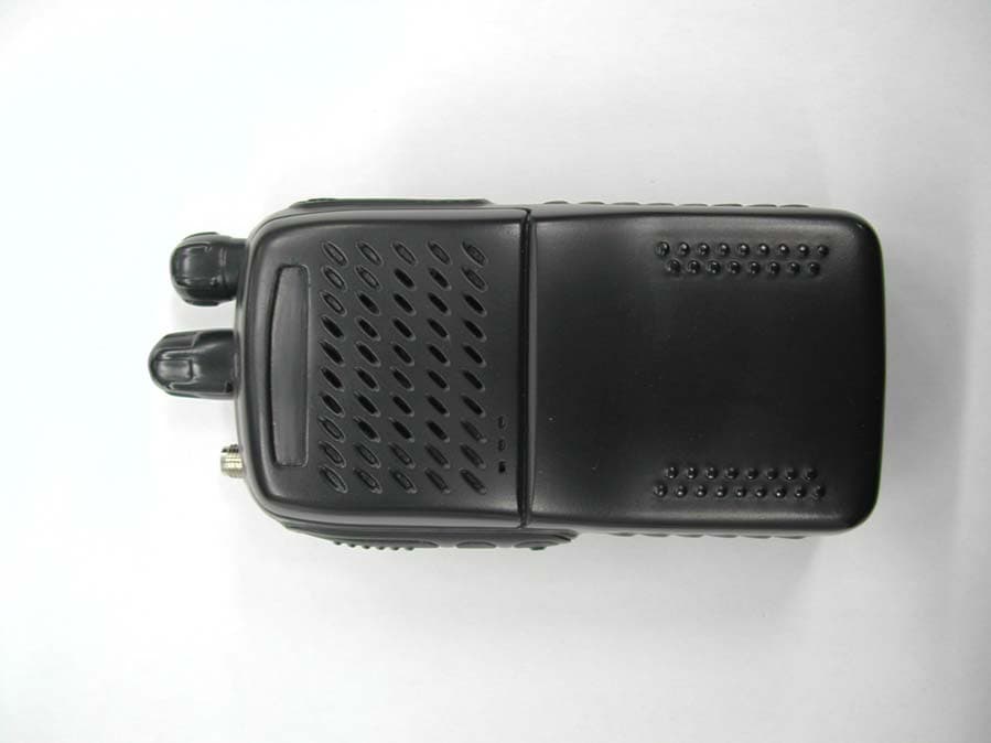
IV9FNCV-70VHF TRANSCEIVER
Kanematsu USA Inc
Click to zoom
Application Details
- Equipment Class
- TNB - Licensed Non-Broadcast Station Transmitter
- Date of Grant
- Oct 30, 2006
- Application Purpose
- Original Equipment
- Date of Application
- Oct 30, 2006
- Equipment Note
- VHF TRANSCEIVER
- Frequency Range
- 150.00000000 - 174.00000000
- Company
- Kanematsu USA Inc
- Country
- United States
Documents & Files
Document Text
Text extracted from the exhibit documents filed with the FCC. Open a document above to read the original.
Block Diagram
1 2 3 4 5 6 78 ABCD 8 7 6 5 4 3 2 1 D CBA Title Number Revision Size A3 Date: 30-Jul-2004 Sheet of File: \\Fs\FS_C\3_‹@Ží•ÊŽ‘—¿\Fennec\F_“d‹CŠÖ ̃AŽ‘—¿\01_Block Diagram\FENNEC_Block.DDB Drawn By: 1st MIX TX VCO RX VCO ANT SW LIMLV TUNE APC TUNE TUNE APC DVDD S_R_M SPC_CHG SPC_CHG CLK/DAT_PUB PLL_STB EXT_PTT DVDD RESET 2TONE DETVOX_CHKDCS_DETSQL_CHK SQL CHK T_A_ML_M_MA_P_MTONE_LEV TCXO PLL LOCK PLL_LOCK DVDD VDD 3.3V RX 8V RX 8V RX 8V RX 8V RX 8V +B ANT B ANT B TX 3V TX 3.3V 8V 8V VDD 3.3V D101/102/402 D103/104 Q101 D105/106 IC402 Q404 Q401 IC403A IC401A D403/405 PWR_CHK PWR_CHK IC403BD404 Temp_CHK Temp_CHK 8V Q404 ANT SW ANT B D107/401 Q102 F201/204 Q201 D202 D203 F203F203 D201 RX 8V CD201 2TONE_DET MIC_SEL IC505 3/4 IC505 2/4 IC505 1/4 IC504 B IC504 A INT MICEXT MIC MIC_LEV Q503/504 IC504 B VDD3.3 5V IC505 4/4 IC503 1/4 IC503 4/4 IC509 2/4 5V SPC_CHG T_A_M IC507 IC505 3/4 Q510/511 VOL1201 Line Out +B IC503 2/4 S_M_M A_P_M S_R_M L_R_M L_M_M VDD 3.3V IC506 B Q505/506 MIN_VOL Q507 5V TONE_LEV Q508 C BEEP IC508 D IC508 A IC508 B IC509 1/4 SPC_CHG IC509 4/4 C_L_1 IC509 3/4 C_L_2 FREQ_ADJ DCSCTCSS +B PWR SW 8V IC701 5V IC702 VDD 3.3V IC703 Q703/704 Q701/702 RX_B IC503 2/4 TX_B RX 8V TX 3.3V V_C VOL1201 5V LCD 8V VOL1201 8V VOL1201 8V VOL1201 8V VOL1201 LCD PWR KEY PWR FRNT LDG FRNT LDR IC1002 LCD CE/DATA/CLK LCD KEY IC1003 DVDD X1001 CTCSS BEEP DTMF FREQ ADJ MOD DCS Vref DAC DATA/CLK/LATCH CLK_PUBEEPROM_SDA IC504 B IC505 4/4 Sub AF Fil IC504 D BUFF AMP BUFF AMPBUFF AMP BPF BPF BUFF AMP RF AMP Pri AMP DRV AMP Power AMP RF AMP ANT LPF ANT SW Power DET SW SW Temp DET 1st IF BPF 2nd IF BPF2nd IF BPF 2nd MIX 2nd Lo Q205 IC201 SW SW Noise AMP Noise DET 2nd IF AMP QUAD DET RSSI_CHK RSSI_CHK Noise H.P.F. ATT ATT RX 8V IC202 B Noise AMP IC202 A NSE SQ TX_B RX_B S_M_M PLL_PDN Q206 SW SWSW SW SW SW SWSW SW MIC AMPMIC AMP AMP AMP AMP AMP SP AMP AMP AMP OSC BPF Splatter Fil AMPAMP AMP LPF Limiter X501 IC502 IC501 A AMP IC501 B AMP DCS_DET 1/N PHASEDET CHG PUMP 1/N PHASEDET CHG PUMP 1/N1/N BUFF DETLOCK SHIFT REG Loop Fil SWSW SW SW SW 8V REG 5V REG 3.3V REG NSE_SQV_C D/A IC1004 LCD driver IC1201 SWSW SWSW RESET EEPROM TONE Fil ATT MIN_VOLCONT VR VOX DET VOX_CHK ATT ATT Gain cont Gain cont Gain cont RX 8V TX 3.3V Q303 Q302 Q305 Q304 X301 D301Q307 D302/Z303 D303/304 Q306 IC301 Q301 8V8V 8V VDD 3.3V VDD 3.3V VDD 3.3V CLK_PUBDAT_PUB Loop Fil PLL_PDN SP AK_STBCLK_PUBDAT_PUB MIC_PTT EXT_HOOK EXT_EMG/LINE OUT EXT_HRN EXT_IGN SW Q1002 C_L_1 C_L_2 MIC_SEL PLL_STB MIC_LEV MIN_VOL VDD 3.3V IC1001 CPU DTMF MOD ANT 5V5V
ID Label/Location Info
ID Label Sample Proposed ID Label Location – Back of the DUT FCC ID: IV9FNCV-70 IC: 5327A-FNCV70 M/N: Fennec VHF70 S/N: XXXX Kanematsu Corporation Made in Malaysia This device complies with part 15 of the FCC Rules Operation is subject to the following two conditions : (1) This device may not cause harmful interference, and (2) this device must accept any interference received , including interference that may cause undesired operation.
Internal Photos
DUT without Case 1 DUT without Case 2 DUT without Case 3 DUT without Case 4 Front PCB 1 Front PCB 2 Main PCB 1 Main PCB 2 Main PCB 3 Main PCB 4 Main PCB 5 VR PCB 1 Main PCB 2 PCB 2
Operational Description
CIRCUIT DESCRIPTION: Fennec VHF,UHF GENERAL INFORMATION The Fennec VHF and UHF has two printed circuit boards; Front board, Radio Frequency and Audio Frequency (RF) board. The Front board contains the Display/Key Input Section. The RF board contains the VCO/Synthesizer section, Transmitter Section, Receiver Section, Transmitter Audio circuitry, the Microprocessor/Control Section. Receiver Audio circuitry. MICROPROCESSOR / CONTROL SECTION The microprocessor IC1001 is constantly operating when the radio is turned ON. It is continuously monitoring The keyboard, the PTT line and other internal inputs such as the squelch detect, etc. When a change occurs, the Microprocessor makes the appropriate response. The microprocessor is used for control. The Radio emits a beep On channel change and the synthesizer is loaded with the correct frequency information. The microprocessor runs off a 19.6608 MHz oscillator which is composed of X1001, C1003, C1004, and R1002. When the radio is first turned on, the microprocessor reads the radio status from the EEPROM IC1003. The microprocessor determines the receive frequency codes, and then loads the synthesizer via its pins 96,97 and 99. VCO / SYNTHESIZER SECTION This section consists of the Temperature-Compensated Crystal Oscillator (TCXO) circuit, Voltage Controlled Oscillators (VCO) circuit, Synthesizer and the Loop Filter. These circuits are found on the RF board. Temperature-Compensated Crystal Oscillator (TCXO) circuit The reference oscillator is a temperature compensated crystal-controlled, Oscillator is held within the specified ±2.5 PPM from -30 to +60 degree C. (X301) Voltage-Controlled Oscillators circuit Only one of the VCOs runs at a time, which is controlled by IC301 and IC1001. When the PTT is pressed, IC1001 pin35 goes High (RX_B) enabling the receive +8V by the Q703 and biases on Q701 to enable the transmitter VCO. The receive VCO consists of C323-C327, L305, and D301, Q304. This VCO oscillates at 45.1 MHz above the programmed receive frequency. The VCO’s oscillating frequency is tuned by the varactor D301. The tuning voltage is supplied from the output of the Loop Filter. The output of the VCO is AC coupled (C317) to the synthesizer and the output buffer Q303 respectively. The output of the VCO buffer Q303 is AC coupled (C317 and R308-R310, C316, C318) to the synthesizer and the output buffer Q302 respectively. The transmitter VCO consists of C339 – C345, C347, C357, C358, L308, L309, Z302, Z303, Q307, D303 . This VCO oscillates on the programmed transmit frequency. The VCO’s oscillating frequency is tuned by the varactor D303. The tuning voltage is supplied from the output of the Loop Filter. The transmit voltage controlled oscillator is directly frequency-modulated and operates on the carrier frequency. In the receive mode, the transmit VCO is disabled and the receive VCO is enabled, producing the receive local oscillator signal at a frequency 45.1MHz above the incoming receive frequency. The synthesizer is tuned in 5.00 kHz or 6.25 kHz step. Synthesizer The frequency synthesizer is a large-scale monolithic synthesizer integrated circuit C301. The synthesizer IC contains a dual modulus prescaler, programmable divide-by-N counter, prescale control (swallow) counter, reference oscillator, reference divider, phase detector, charge pump and lock detector. Also, included in IC301 are shift registers and control circuits for frequency controls and general device control. RF output from the active VCO is AC coupled to the synthesizer IC301 prescaler input at Pin 13. The divide counter chain in IC301, consisting of the dual-modulus prescaler, swallow counter and programmable counter, divides the VCO signal down to a frequency very close to 5.00 kHz or 6.25kHz which is applied to the phase detector. The phase comparator compares the phase with the 5.00kHz or 6.25kHz reference signal from the reference divider and drives the charge pump. The synthesizer unlock detector circuit prevents the operation of the transmitter and receiver, when the phase lock loop (PLL) is unlocked. The following discussion assumes the unit has been placed in the transmit mode. IC301 lock detector Pin 6 goes high when the PLL is locked. This high level is applied to Pin 98 of the microprocessor IC1001. A software timing routing brings the TX line High (Pin 47 of IC1001). With the TX line low, Q702 is cut off and Q208 is biases on passing +5VTX-B to Q202, it biases on IC701 to pass switched TX-B to the transmitter amplifier staring which enables transmission. When the PLL become unlocked, the lock detector at IC301 Pin6 will begin pulsing low. A RC circuit converts pulsing low to a low level for the microprocessor. The microprocessor then changes the TX_B line to a low, thus signaling the other transistor switches to drive Q702 into cutoff which disable transmission. Therefore, the transmitter remains disabled while the loop remains out of lock and “PLL ERR” is displayed. Loop Filter The Loop Filter, a passive lead-lag filter consisting of R317- R322 and C332 - C335, integrates the charge pump output to produce the DC turning voltage for the VCO. One parasitic pole, consisting of RFchokes L306/L307, Prevent modulation of the VCOs by the 5.00 kHz or 6.25 kHz reference energy remaining at the output of the loop filter. Direct FM is obtained for modulating frequencies outside the PLL bandwidth by applying the CTCSS/DCS signals and the pre-emphasized, limited microphone audio to the VCO modulation circuit. The modulation circuit consists of R326, R327and D304. TRANSMITTER SECTION RF POWER Amplifier After the PTT is pressed, the RX 8V off and +3.3VTX-B line switches to approximately 3.3V. Q305 is turned off enabling transmit VCO. The VCO buffer, pre-driver, driver and power amplifier are biased on by Q701, which is biased on by the TX 3.3V line switching to 3.3V. RF output from the transmit VCO (Q307) is applied to the VCO output buffer Q303, Q301. Output from Q303, Q301 feeds th…
Text truncated - open the document above for the full version.
Parts List/Tune Up Info
FENNECALIGNMENT 1) POWER ALIGNMENT NO. PROCESS DESCRIPTION 1 "CONNECT FRONT LCD DISPLAY , VOLUME CONTROL PCB , PROGRAMMING CABLE AND ANTENNA CABLE." 2 "SWITCH ""ON"" THE POWER." 3 CHECK THE POWER ACROSS CH1 ~ CH6 BY PTT AT EVERY CH. 4 "OPEN ""FennecWin.exe""." 1 POWER ALIGNMENT 1.1. "OPEN ""FennecWin.exe"" AND SELECT DEALER" "i) CLICK ""Dealer"" AT HEADER MANUAL AND AFTER CLICK ON ""Alignment"" " "ii) WAIT UNTIL DISPLAY ""Upload Completed"" AND ""Adjustment"" DIALOG BOX DISPLAY ." "iii) ALIGNMENT THE HIGH POWER FOR CH1 ~ CH3 BY CHANGING THE SOFTPOT AT "" Tx_P High (Wide) "" AND CLICK ""OK""." iv) CONFIRM THE POWER READING FROM HP8920. v) IF THE POWER ALREADY IN SPEC. THEN CONTINUE STEP (vi) ; IF NOT BACK TO ( i~iv) vi) CLICK ""Dealer"" AT HEADER MANUAL AND AFTER CLICK ON ""Alignment"" " vii) WAIT UNTIL DISPLAY ""Upload Completed"" AND ""Adjustment"" DIALOG BOX DISPLAY ." viii) ALIGNMENT THE LOW POWER FOR CH4 ~ CH6 BY CHANGING THE SOFTPOT AT "" Tx_P Low (Wide) "" AND CLICK ""OK""." ix) CONFIRM THE POWER READING FROM HP8920. x) IF THE POWER ALREADY IN SPEC. THEN CONTINUE STEP (xi) ; IF NOT BACK TO ( vi~ix) xi) TEST END REMARKS :MAKESURE ATTENUETOR IS ATTACH. (20dB ; 50W) 2 VCO CHECK & ALIGNMENT NO. PROCESS DESCRIPTION 1 VCO CHECK & ALIGNMENT 1. """ON"" POWER BY TURNING VOL1201 AT VOL CONTROL PCB." 2. "LCD WILL DISPLAY ""CH 001"" " 3. "SET THE CHANNEL TO ""CH 003""." 4. CHECK THE RX VCO VOLTAGE FROM THE MULTIMETER. SPEC - RX VCO = 3.0 Vdc ~ 3.2 Vdc i) For VHF ONLY CONFIRMATION AND UHF HAVE TO ALIGN. ii) ADD SILICON (TSE 399) UHF ALIGN BY OPENING L305 AIRCOIL. 5. "CHECK THE TX VCO VOLTAGE BY TURN ""ON"" THE PTT SWITCH AT THE TEST BOX." SPEC - TX VCO = 3.0 Vdc ~ 3.2Vdc i) For VHF ONLY CONFIRMATION AND UHF HAVE TO ALIGN. ii) ADD SILICON (TSE 399) AND UHF ALIGN BY OPENING L309 AIRCOIL. 6. "TURN ""OFF"" PTT SWITCH. " 3 TX FREQ. ALIGNMENT 1. "TURN ""ON"" PTT SWITCH AT TEST BOX." 2. CHECK THE FREQ. ERR. AT THE HP 8920 SPEC - FREQ ERR = -50 Hz TO 50 Hz. 3. "ALIGN THE BY USING ""FennecWIN.exe"". " "i) CLICK ""Dealer"" AT HEADER MANUAL AND AFTER ""Alignment"" " "ii) WAIT UNTIL DISPLAY ""Upload Completed"" AND ""Adjustment"" DIALOG BOX DISPLAY ." "iii) SELECT THE ""TX Limit""." "vi) CHANGE THE VALUE AT ""CDCSS Decode center Level"" TO GET " 4 TX MODULATION ALIGNMENT 1. "CHECK CH 1 TO CH 3 THE READ OF THE MODULATION BY TURN ""ON"" PTT WHEN SWITCH CH." 2. "TURN ""OFF"" PTT SWITCH. " 3. "CHANGE THE VALUE AT ""AK 2345 Limit"" TO GET THE BEST READING." SPEC - STANDARD MODULATION = 4.5KHz ~ 4.6KHz 5 TX DCS & CTCSS ALIGNMENT 1. SET THE CH TO CH 007 TO ALIGN DCS. 2. "TURN ""ON"" PTT SWITCH AT TEST BOX." 3. ALIGN VR301 GET THE SQUARE WAVEFORM AT OSCILLOSCOPE AS FLAT AS POSSIBLE. 4. SET THE CH TO CH 008 TO ALIGN CTCSS. 5. ALIGN VR501 GET CTCSS IN SPEC. SPEC - CTCSS = 0.700 KHz ~ 0.800KHz 6. """OFF"" POWER AND REMOVE PCB FROM FIXTURE." 7. END TEST NOTICE : "SWITCH ""OFF"" FIXTURE POWER SUPPLY SWITCH FIRST BEFORE REMOVE PCB FROM FIXTURE. " TEST ITEM 6 RX TEST NO. PROCESS DESCRIPTION 1 Connect the Antenna & Power Cable. 2 """ON"" POWER BY TURNING VOL1201 AT VOL CONTROL PCB, DISPLAY WILL SHOW CH 001." 3 TURN THE VOL CONTROL TO GET 3.5 Vac +/- 0.3 FROM AC VOLTMETER. 4 CONFIRM THE SINAD > 12dBm FROM THE SINAD METER. 5 CHANGE THE CHANNEL FROM CH 001~ CH 006 AND THE REG 01~ REG 06 TO CONFIRM THE SINAD RESPECTIVELY 6 MARK THE UUT UNIT AFTER CONFIRMED WITHIN THE SPEC. 7 CONTINUE THE STEP 1~6 FOR THE NEXT UNIT. REMARKS :"IT IS CONSIDERED PASS EVEN THOUGHT ""INST PK+"" OR ""INST PK-"" FAILED. "
Parts List/Tune Up Info
VHF 70W Front PCB Parts List 1 / 1 SymbolParts NameDescription PCBK411E511-03MiMo Disp&Vol PCB : 20pcs per 1sheet C1201GRM1882C1H101JA01DCeramic Chip Capacitor: 1608/100pF/CH/50V C1202GRM188B11H103KA01DCeramic Chip Capacitor: 1608/0.010uF/B/50V C1203GRM188B11E104KA01DCeramic Chip Capacitor: 1608/0.1uF/B/50V C1204Not useNot use C1205Not useNot use C1206Not useNot use C1207GRM1882C1H681JA01Ceramic Chip Capacitor: 1608/680pF/CH/50V C1208GRM188B11E104KA01DCeramic Chip Capacitor: 1608/0.1uF/B/50V CN120152559-1292Connectors CN120352745-1490Connectors D1201VRPG3312XLED D1202FA1101FLED D1203FA1101FLED D1204TLOU1008ALED D1205TLOU1008ALED D1206TLOU1008ALED D1207TLOU1008ALED D1208TLOU1008ALED D1209TLOU1008ALED FFC1FBNCD-P=0.5-K1-14-170FFC Cable FFC2FBNCD-P=0.5-K1-12-170 3/5BLULFFC Cable IC1201LC75854WIC : LCD Driver J1201R41-2509-HModular Jack LCD1201LCMTR201Z-1B/TTR7966UPFDCNLiquid Crystal Display Module Q1201SSM3K16FS(TE85L)Digital Transistor Q1202SSM3K16FS(TE85L)Digital Transistor Q1203SSM3K16FS(TE85L)Digital Transistor Q1204DTC144EE-T146(26)Digital Transistor Q1205DTC144EE-T146(26)Digital Transistor Q1210DTC114EE TLDigital Transistor Q1211DTC114EE TLDigital Transistor Q1212DTC114EE TLDigital Transistor R1201CR1/16-391JVChip Resistor : 1608/390Ω/J R1202CR1/16-391JVChip Resistor : 1608/390Ω/J R1203CR1/16-221JVChip Resistor : 1608/220Ω/J R1204CR1/16-102JVChip Resistor : 1608/1.0kΩ/J R1205CR1/16-222JVChip Resistor : 1608/2.2kΩ/J R1206CR1/16-222JVChip Resistor : 1608/2.2kΩ/J R1209CR1/16-102JVChip Resistor : 1608/1.0kΩ/J R1210CR1/16-102JVChip Resistor : 1608/1.0kΩ/J R1211CR1/16-102JVChip Resistor : 1608/1.0kΩ/J R1212CR1/16-623JVChip Resistor : 1608/62kΩ/J R1213CR1/16-104JVChip Resistor : 1608/100kΩ/J R1214CR1/16-104JVChip Resistor : 1608/100kΩ/J R1215CR1/16-104JVChip Resistor : 1608/100kΩ/J R1217Not useNot use R1218Not useNot use R1219CR1/16-104JVChip Resistor : 1608/100kΩ/J R1220CR1/16-104JVChip Resistor : 1608/100kΩ/J R1221Not useNot use R1222Not useNot use R1223Not useNot use R1224Not useNot use R1225CR1/16-000JVChip Resistor : 1608/ 0 Ω/J R1226Not useNot use SP1C062SBX017Z00/C062SB501-10Speaker : 8Ω VOL1201RH76N74N 10K ASwich VR W901SPK-Wire-Assy-50WWire : Speaker VHF 70W Main PCB Parts List 1 / 8 SymbolParts NameDescription PCBK411E510-05Mimo Main PCB : 2pcs per 1 sheet. C101 GRM21B2C2D221JY21DCeramic Chip Capacitor: 2012/220pF/CH/200V C102 GRM1882C2D100JV01DCeramic Chip Capacitor: 1608/10pF/CH/200V C103 GRM1882C2D4R0CV01DCeramic Chip Capacitor: 1608/4.0pF/CH/200V C104 GRM1882C2D4R0CV01DCeramic Chip Capacitor: 1608/4.0pF/CH/200V C105 GRM2192C2D120JV01DCeramic Chip Capacitor: 20085/12pF/CH/200V C106 GRM2192C2D150JV01DCeramic Chip Capacitor: 20085/15pF/CH/200V C107 GRM2192C2D180JV01DCeramic Chip Capacitor: 20085/18pF/CH/200V C108 GRM2192C2D150JV01DCeramic Chip Capacitor: 20085/15pF/CH/200V C109 GRM1882C1H150JZ01DCeramic Chip Capacitor: 1608/15pF/CH/50V C110Not useNot use C111GRM188B11H102KA01DCeramic Chip Capacitor: 1608/1000pF/B/50V C112GRM188B11H102KA01DCeramic Chip Capacitor: 1608/1000pF/B/50V C113Not useNot use C114GRM1882C1H080JZ01DCeramic Chip Capacitor: 1608/8.0pF/CH/50V C115GRM188B11H102KA01DCeramic Chip Capacitor: 1608/1000pF/B/50V C116GRM1882C1H2R0CZ01DCeramic Chip Capacitor: 1608/2.0pF/CH/50V C117 Not useNot use C118GRM188B11H102KA01DCeramic Chip Capacitor: 1608/1000pF/B/50V C119GRM188B11H102KA01DCeramic Chip Capacitor: 1608/1000pF/B/50V C120GRM188B11H102KA01DCeramic Chip Capacitor: 1608/1000pF/B/50V C121GRM188B11H102KA01DCeramic Chip Capacitor: 1608/1000pF/B/50V C122GRM1882C1H2R0CZ01DCeramic Chip Capacitor: 1608/2.0pF/CH/50V C123GRM188B11H102KA01DCeramic Chip Capacitor: 1608/1000pF/B/50V C124GRM1884C1HR50CZ01DCeramic Chip Capacitor: 1608/0.5pF/CK50V C125GRM188B11H102KA01DCeramic Chip Capacitor: 1608/1000pF/B/50V C126GRM1882C1H2R0CZ01DCeramic Chip Capacitor: 1608/2.0pF/CH/50V C127GRM188B11H102KA01DCeramic Chip Capacitor: 1608/1000pF/B/50V C128GRM188B11C104KA01DCeramic Chip Capacitor: 1608/0.10uF/B/16V C129GRM1882C1H5R0CZ01DCeramic Chip Capacitor: 1608/5.0pF/CH/50V C130 GRM188B11H102KA01DCeramic Chip Capacitor: 1608/1000pF/B/50V C131GRM188B11H102KA01DCeramic Chip Capacitor: 1608/1000pF/B/50V C132GRM188B11H103KA01DCeramic Chip Capacitor: 1608/0.010uF/B/50V C133GRM1882C1H560JZ01Ceramic Chip Capacitor: 1608/56pF/CH/50V C134GRM188B11H102KA01DCeramic Chip Capacitor: 1608/1000pF/B/50V C135GRM188B11H103KA01DCeramic Chip Capacitor: 1608/0.010uF/B/50V C136GRM188B11H103KA01DCeramic Chip Capacitor: 1608/0.010uF/B/50V C137GRM188B11H102KA01DCeramic Chip Capacitor: 1608/1000pF/B/50V C138GRM1884C1HR50CZ01DCeramic Chip Capacitor: 1608/0.5pF/CK50V C139Not useNot use C201GRM1882C1H4R0CZ01DCeramic Chip Capacitor: 1608/4.0pF/CH/50V C202GRM1882C1H100JZ01DCeramic Chip Capacitor: 1608/10pF/CH/50V C203GRM1882C1H270JZ01DCeramic Chip Capacitor: 1608/27pF/CH/50V C204GRM188B11H103KA01DCeramic Chip Capacitor: 1608/0.010uF/B/50V C205Not useNot use C206GRM188B11H102KA01DCeramic Chip Capacitor: 1608/1000pF/B/50V C207GRM188B11H103KA01DCeramic Chip Capacitor: 1608/0.010uF/B/50V C208SK7-0J336M-RAChip Tantalum Electrolytic Capacitor : 33uF/6.3V/A_Case C209GRM188B11C104KA01DCeramic Chip Capacitor: 1608/0.10uF/B/16V C210GRM188B11C104KA01DCeramic Chip Capacitor: 1608/0.10uF/B/16V C211GRM188B11C104KA01DCeramic Chip Capacitor: 1608/0.10uF/B/16V C212GRM1882C1H101JA01DCeramic Chip Capacitor: 1608/100pF/CH/50V C213SK-1V224M-RAChip Tantalum Electrolytic Capacitor : 0.22uF/35V/A_Case C214GRM188B11H103KA01DCeramic Chip Capacitor: 1608/0.010uF/B/50V C215GRM1882C1H5R0CZ01DCeramic Chip Capacitor: 1608/5.0pF/CH/50V C216GRM1882C1H6R0CZ01DCeramic Chip Capacitor: 1608/6.0pF/CH/50V C217GRM1882C1H220JZ01DCeramic Chip Capacitor: 1608/22pF/CH/50V C218GRM1882C1H330JA01DCeramic Chip Capacitor: 1608/33pF/CH/50V C219GRM1882C1H150JZ01DCeramic Chip Capacitor: 1608/15pF/CH/50V C220GRM188B11C104KA01DCeramic Chip Capacitor: 1608/0.10uF/B/16V C221GRM188B11H103KA01DCeramic Chip Capacitor: 1608/0.010uF/B/50V C222GRM188B11C104KA01DCeramic Chip Capacitor: 16…
Text truncated - open the document above for the full version.
RF Exposure Info
Applicant: Kanematsu USA Page 1 of 3 FCC ID: IV9FNCV-70 FCC RF Exposure Requirements General information FCC ID: IV9FNCV-70 Device category: Mobile per Part 2.1091 Environment: Controlled Exposure Mobile devices that operate under Part 90 of this chapter are subject to routine environmental evaluation for RF exposure prior to equipment authorization or use if they operate at frequencies of 1.5 GHz or below and their effective radiated power (ERP) is 1.5 watts or more. However, compliance with the power density limits of 1.1310 is not required. Antenna The manufacturer does not specify any antenna to be used with this device. This device has provisions for operation in a vehicle, or a fixed location. Configuration Antenna p/n Type Max. Gain (dBi) Passenger car Any omni 5 Operating configuration and exposure conditions The conducted output power is 72 watts. Typical use qualifies for a maximum duty cycle factor of 50%. The manufacturer also markets this device only for occupation use. - Vehicle Operation: The maximum antenna gain that can be used is 5dBi or 3 dBd. A coaxial cable of the type RG 58 has a loss of 1dB for a length of 15 feet. MPE Calculation : The minimum separation distance is calculated as follows: The limit for occupation/controlled exposure environment below 300 MHz is 1 mW/cm 2 . Applicant: Kanematsu USA Page 2 of 3 FCC ID: IV9FNCV-70 Channel frequency: 134-174 MHz The conducted power output is 72.4 watt. The coax loss was taken as 1 dB. Antenna gain was taken as 3 dBd 50% talk time f300:= Frequency in MHz CL1:= coax loss uncontrolled exposure GdBd2.15+CL−:= G4.15= net-gain in dBi S f 300 := gain numeric Gn10 G 10 :=S1= mW cm 2 Gn2.6= R Po Gn⋅() 4π⋅S⋅ () :=Rinches R 2.54 := R86.606= distance in centimeters Rinches34.097= required for compliance W72.5:= power in Watts D1:= Duty Factor in decimal % (1=100%) E3.0:= exposure time in minutes U6:= (use 6 for controlled and 30 for uncontrolled ) WexpW D⋅ E U ⎛ ⎜ ⎝ ⎞ ⎠ ⋅:=PC E U := PC0.5= percent on time Wexp36.25=Watts Power outputantenna gainCalculation of S Po36250:=mWattsdBd3:= Applicant: Kanematsu USA Page 3 of 3 FCC ID: IV9FNCV-70 Conclusion The device complies with the MPE requirements by providing a safe separation distance of 86.6 cm between the antenna, including any radiating structure, and any persons when normally operated. Proposed RF exposure safety information to include in User’s Manual “FCC RF Exposure Requirements: CAUTION: The antenna(s) used for this transmitter must not be co-located or operating in conjunction with any other antenna or transmitter. This device is approved with emissions having a source-based time-averaging duty factor not exceeding 50%. Vehicle – Antenna Installation: - Antennas used for this transmitter must not exceed an antenna gain of 5 dBi with a minimum cable loss of 1dB. - For rear deck trunk and roof top installations, the antenna must be located at least 86.6 cm away from rear-seat passengers and bystanders in order to comply with the FCC RF exposure requirements. The following label will be mounted in conspicuous view on the radio. Failure to observe these restrictions will result in exceeding the FCC RF exposure limits.
Test Report
FCC PART 90 TEST REPORT APPLICANT KANEMATSU USA INC. 543 WEST ALGONQUIN ROAD ARLINGTON HEIGHTS ILLINOIS 60005 USA FCC ID IV9FNCV-70 MODEL NUMBER Fennec VHF70 PRODUCT DESCRIPTION VHF TRANSCEIVER DATE SAMPLE RECEIVED 7/28/2006 DATE TESTED 8/15/2006 TESTED BY Nam Nguyen APPROVED BY Mario de Aranzeta TIMCO REPORT NO. 2235AUT6TestReport TEST RESULTS PASS FAIL THE ATTACHED REPORT SHALL NOT BE REPRODUCED EXCEPT IN FULL WITHOUT THE WRITTEN APPROVAL OF TIMCO ENGINEERING, INC. 849 NW STATE ROAD 45 NEWBERRY, FL 32669 USA PH: 888.472.2424 OR 352.472.5500 FAX: 352.472.2030 EMAIL: [email protected] HTTP: //WWW.TIMCOENGR.COM Certificate # 0955-01 Applicant: KANEMATSU USA INC. FCC ID: IV9FNCV-70 Report: K\KANEMATSU USA_\2235AUT6\2235AUT6TestReport.doc Page 2 of 24 TABLE OF CONTENTS STATEMENT OF COMPLIANCE ....................................................................... 3 GENERAL INFORMATION ............................................................................... 4 TEST EQUIPMENT .......................................................................................... 5 TEST PROCEDURE ......................................................................................... 6 TEST RESULT................................................................................................. 9 RF POWER OUTPUT ............................................................................................................. 9 MODULATION CHARACTERISTICS..................................................................................... 10 OCCUPIED BANDWIDTH .................................................................................................... 14 SPURIOUS EMISSIONS AT ANTENNA TERMINALS (CONDUCTED) ..................................... 17 FIELD STRENGTH OF SPURIOUS EMISSIONS ................................................................... 18 FREQUENCY STABILITY..................................................................................................... 20 TRANSIENT FREQUENCY BEHAVIOR................................................................................. 21 POWER LINE CONDUCTED INTERFERENCE ..................................................................... 24 Applicant: KANEMATSU USA INC. FCC ID: IV9FNCV-70 Report: K\KANEMATSU USA_\2235AUT6\2235AUT6TestReport.doc Page 3 of 24 STATEMENT OF COMPLIANCE This equipment has been tested in accordance with the standards identified in the referenced test report. To the best of my knowledge and belief, these tests were performed using the measurement procedures described in this report and demonstrate that the equipment complies with the appropriate standards. No modifications were made to the equipment during testing in order to demonstrate compliance with these standards. I attest that the necessary measurements were made by me or under my supervision, at Timco Engineering, Inc. located at 849 N.W. State Road 45, Newberry, Florida 32669 USA. Authorized by: Mario de Aranzeta Signature: On File Function: Engineer Date: September 26, 2006 Tested by: Nam Nguyen Signature: on file Date: August 15, 2006 Applicant: KANEMATSU USA INC. FCC ID: IV9FNCV-70 Report: K\KANEMATSU USA_\2235AUT6\2235AUT6TestReport.doc Page 4 of 24 GENERAL INFORMATION Test System Information Disclaimer : The test results relate only to the items tested. Purpose of Test : To show the DUT in compliance with FCC CFR 47, Part 90 requirements for VHF radios. Test Standards : TIA 603, FCC CFR 47 Part 90, ANSI C63.4: 2003, Related Report : 2235BUT6TestReport for digital interface portion Test Facility : RF output power and radiated emission were conducted by Timco Engineering Inc. located at 849 NW State Road 45, Newberry, FL 32669 USA Laboratory Test Condition : The temperature was 26ºC with a relative humidity of 50%. Modification to the DUT : No modification was made to ensure the DUT complaint with requirements. Test Exercise : The DUT was placed in continuous transmit mode of operation. System Setup : Stand alone device. Product Specification DUT : VHF TRANSCEIVER FCC ID : IV9FNCV-70 M/N : Fennec VHF70 S/N : N/A Operating Freq : 150 ~ 174 MHz Max. Output Pwr : High: 72W, Low: 10W Channel Spacing : 12.5 kHz, 25 kHz No. of Channels : Single Emission Designator(s) : 10K8F3E Calculation of Designator(s) : Bn = 2M + 2DK, M = 3000, D = 2440 K=1 Bn = 2(3000) + 2(2440) = 10.88 Modulation : FM Power Source : Battery Operated Exclusively Test Item : Pre-production Type of DUT : Mobile Antenna Spec : OMNI, 5 dBi Applicant: KANEMATSU USA INC. FCC ID: IV9FNCV-70 Report: K\KANEMATSU USA_\2235AUT6\2235AUT6TestReport.doc Page 5 of 24 TEST EQUIPMENT Device Manufacturer Model Serial Number Cal/Char Date Due Date Analyzer Tan Tower Spectrum Analyzer HP 8566B Opt 462 3138A07786 3144A20661 CAL 12/7/05 12/7/07 Analyzer Tan Tower RF Preselector HP 85685A 3221A01400 CAL 12/7/05 12/7/07 Analyzer Tan Tower Quasi-Peak Adapter HP 85650A 3303A01690 CAL 12/8/05 12/8/07 Analyzer Tan Tower Preamplifier HP 8449B- H02 3008A00372 CAL 12/8/05 12/8/07 Antenna: Biconnical Electro- Metrics BIA-25 1171 CAL 4/29/05 4/29/07 Antenna: Double- Ridged Horn Electro- Metrics RGA- 180 2319 CAL 12/29/04 12/29/06 Termaline Wattmeter Bird Electronic Corporation 611 16405 CAL 7/16/06 7/16/08 Applicant: KANEMATSU USA INC. FCC ID: IV9FNCV-70 Report: K\KANEMATSU USA_\2235AUT6\2235AUT6TestReport.doc Page 6 of 24 TEST PROCEDURE Power Line Conducted Interference The procedure used was ANSI 63.4-2003 using a 50uH LISN. Both lines were observed with the UUT transmitting. The bandwidth of the spectrum analyzer was 10 kHz with an appropriate sweep speed. RF Power Output The RF power output was measured at the antenna feed point using a peak power meter. A 50-ohm, resistive wattmeter was connected to the RF output connector. With a nominal battery voltage, and the transmitter properly adjusted the RF output measures: Spurious Emissions At Antenna Terminals (Conducted) The carrier was modulated 100% using a 2500 Hz tone. The spe…
Text truncated - open the document above for the full version.
Test Report
FCC PART 90 SUPPLEMENT TEST REPORT APPLICANT KANEMATSU USA INC. 543 WEST ALGONQUIN ROAD ARLINGTON HEIGHTS ILLINOIS 60005 USA FCC ID IV9FNCV-70 MODEL NUMBER Fennec VHF70 PRODUCT DESCRIPTION VHF TRANSCEIVER DATE SAMPLE RECEIVED 7/28/2006 DATE TESTED 8/15/2006 TESTED BY Nam Nguyen APPROVED BY Mario de Aranzeta TIMCO REPORT NO. 2235AUT6TestReport Supplement TEST RESULTS PASS FAIL THE ATTACHED REPORT SHALL NOT BE REPRODUCED EXCEPT IN FULL WITHOUT THE WRITTEN APPROVAL OF TIMCO ENGINEERING, INC. 849 NW STATE ROAD 45 NEWBERRY, FL 32669 USA PH: 888.472.2424 OR 352.472.5500 FAX: 352.472.2030 EMAIL: [email protected] HTTP: //WWW.TIMCOENGR.COM Certificate # 0955-01 Certificate # 0955-01 Applicant: Kanematsu USA FCC ID: IV9FNCV-70 Report: V:\K\KANEMATSU USA_\2235AUT6\2235AUT6TestReport Supplement.doc Page 2 of 3 TABLE OF CONTENTS PRODUCT SPECIFICATION ............................................................................. 3 Certificate # 0955-01 Applicant: Kanematsu USA FCC ID: IV9FNCV-70 Report: V:\K\KANEMATSU USA_\2235AUT6\2235AUT6TestReport Supplement.doc Page 3 of 3 PRODUCT SPECIFICATION Purpose of Report : To list 2 nd emission designator DUT : VHF TRANSCEIVER FCC ID : IV9FNCV-70 M/N : Fennec VHF70 S/N : N/A Operating Freq : 150 ~ 174 MHz Max. Output Pwr : High: 72W, Low: 10W Channel Spacing : 12.5 kHz, 25 kHz No. of Channels : Single Emission Designator(s) : 10K8F3E 15K7F3E Calculation of Designator(s) : Bn = 2M + 2DK, M = 3000, D = 2440 K=1 Bn = 2(3000) + 2(2440) = 10.88 Bn = 2M + 2DK, M = 3000, D = 4880 K=1 Bn = 2(3000) + 2(4880) = 15.76 Modulation : FM Power Source : Battery Operated Exclusively Test Item : Pre-production Type of DUT : Mobile Antenna Spec : OMNI, 5 dBi
Contact Information
Applicant
Masa Nishikawa(Manager)
Test Firm
Timco Engineering, Inc.Sid Sanders
Technical Specifications
| # | Rule Parts | Frequency Range | Power Output | Emission | Tolerance |
|---|---|---|---|---|---|
| 4 | 9 | 150 MHz - 174 MHz | 10 W | 15K7F3E | 2.5 ppm |
Other Applications from Kanematsu USA Inc
IV9BSHH16V
Dec 30, 2004VHF Transceiver
Equipment Class
TNF - Licensed Non-Broadcast Transmitter Held to Face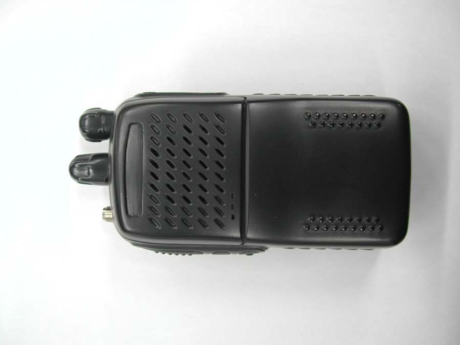
IV9BSHH16U
Dec 30, 2004UHF Transceiver
Equipment Class
TNF - Licensed Non-Broadcast Transmitter Held to Face
IV9FNCU-M45
Sep 27, 200445W UHF RADIO
Equipment Class
TNB - Licensed Non-Broadcast Station Transmitter
IV9FNCU-H45
Sep 20, 2004UHF TRANSCEIVER
Equipment Class
TNB - Licensed Non-Broadcast Station Transmitter
IV9FNCV-50
Aug 26, 2004VHF TRANSCEIVER
Equipment Class
TNB - Licensed Non-Broadcast Station Transmitter