IV9FNCV-50VHF TRANSCEIVER
Kanematsu USA Inc
Click to zoom
Application Details
- Equipment Class
- TNB - Licensed Non-Broadcast Station Transmitter
- Date of Grant
- Aug 26, 2004
- Application Purpose
- Original Equipment
- Date of Application
- Aug 26, 2004
- Equipment Note
- VHF TRANSCEIVER
- Frequency Range
- 134.00000000 - 174.00000000
- Company
- Kanematsu USA Inc
- Country
- United States
Documents & Files
Document Text
Text extracted from the exhibit documents filed with the FCC. Open a document above to read the original.
Users Manual
F-25V/F-25U/F-50V/F-45U Operating Manual INTRODUCTION This Manual describes the operation for the Kanematsu Land mobile radio This Land Mobile is full-featured FM transceiver designed for flexible mobile and base station business communications in the VHF or UHF Land mobile bands. This Land mobile radio can be programmed with 128 channels. This Land mobile include a 16 segment, 8character, numeric display for channel display. Important channel frequency data is stored in EEPROM and flash memory on the CPU, and easily programmable by dealers using personal computer and PC EDITER software. FCC Requirements Your radio must be properly licensed Federal Communications Commission prior to use. Your Wireless dealer can assist you in meeting these requirements. Your dealer will program each radio with your authorized frequencies, signaling codes, etc., and will be there to meet your communications needs as your system expands. SAFETY WANING INFORMATION READ THIS IMPORTANT INFORMATION ON SAFE AND EFFICIENT OPERATION BEFORE USING YOURLANDMOBILERADIO Only qualified technicians are allowed to repair this product. Do not operate the radio without a proper antenna attached. As this may damage the radio and may also cause to exceed FCC RF exposure limits. Typical electronic systems that may malfunction due to the lack of protection from radio frequency energy present when transmitting. If the vehicle contains such equipment, consult the dealer. Just as it is dangerous to fuel a vehicle with motor running, similar hazard exist when operation a mobile radio. Be sure to turn the radio off while fueling a vehicle. Do not operate the radio without a proper antenna attached, as this may damage the radio and may also cause you to exceed FCC RF exposure limits. Do not transmit for more than 50% of total radio use time. Transmitting more than 50% of the time can cause FCC RF exposure compliance requirements to be exceeded. Always Keep at least 25cm (10inches) between the antenna and operator while transmitting. Always use authorized accessories. Dynamite blasting caps may be caused to explode by operating a radio within 500 feet of the blasting caps. Always obey the “Turn Off Two –Way radios” signs posted where dynamite is being used. Do not install the radio in the closed compartment that contains an LP gas container or its fitting. No changes or adjustments shall be made to the equipment except by an authorized or certified electronic technician. Using your radio to send personal messages is a violation of FCC rules. Control and Connectors FRONT PANEL All Buttons on the Front Panel are Programmable Function (PF) Buttons, configured according to your network requirements and programmed by your dealer. The instructions below a typically configured radio 1 VOL/PWR Knob Turn this control clockwise to turn the radio on and increase the volume. Turn it counterclockwise into the click-stop to the radio off. 2 BUSY/TX Indicator Indicate transceiver Transmit/Receive Status Steady Red: Transmitting in progress Steady Green: Busy Channel 3 UP/DOWN Buttons (Programmable Function Buttons) Pressing either button changes the current channel (and displayed name). 4 LCD The display includes and 8-character alphanumeric section showing channel names, status and identity information, and error messages. 5 Microphone Jack Connect the microphone plug to this jack. 6 [P]-[C] Buttons (Programmable Function Buttons) These buttons can be set up for the special applications, such as High/Low power selection, Monitor, Talk-Around, etc as determined by your network requirements and programmed by dealer. LCD Icons & Indicators REAR PANEL 1Antenna Socket The 50-ohm coaxial feed line to the antenna must be connected here, using a Type-M (PL-259) plug. 2 13.8V DC Cable Pigtail with connector The supplied DC power cable must be connected to this 2-contact. Use only the supplied fused cable, extended if necessary, for power connection. 3 External Speaker Jack An external loudspeaker may be connected to this 2-contact, 3.5mm mini-phone jack Caution: Do not connect either wire of this line to ground, and be certain that the speaker has adequate capability to handle the audio output (4W) from the radio. 4 D-Sub 15-Pin Accessory Connector External TX audio line input, PTT (Push To Talk), and external RX audio Line output signals may be obtained from this connector for use with accessories such as data transmission. BASICOPERATION Important!– Before turning on the radio the first time, confirm that the power connections have been made correctly and that a proper antenna is connected to the antenna jack. Overview - Your authorized Dealer can program your radio for Conventional format. RECEIVE Switching Power ON Turn power on by the VOL/PWR knob. The radio will beep, and become illuminated. Press the UP/DOWN button to choose the desired operating channel. A channel name will appear on the display. Setting the volume Turn the VOL/PWR knob clockwise to increase the volume, and counterclockwise to decrease it. Select a Channel Press the assigned PF button to Up/down Channel. The display can show channel numbers or channel labels. Technician along programs the display mode and channel labels. Transmitting Press PF button, which is programmed to the Monitor feature to listen for channel activity When receiving a call, transmit only after the incoming call ends. The radio cannot receive a call and transmit simultaneously. Press PTT switch. If the channel is clear, the BUSY/TX indicator will grow red. The radio is now transmitting. While holding in the PTT switch, speak across the face of the microphone in a clear and normal voice. For best transmission, hold the microphone about 1-1/2 to 2 inches away from your mouth. Release the PTT switch to receive. If the Busy Channel Lockout feature has been programmed on a channel, the radio will not transmit when a carrier is present. Instead, the radio will generate a continuous low-pitched tone while PTT switch i…
Text truncated - open the document above for the full version.
Operational Description
CIRCUIT DESCRIPTION: Fennec VHF,UHF GENERAL INFORMATION The Fennec VHF and UHF has two printed circuit boards; Front board, Radio Frequency and Audio Frequency (RF) board. The Front board contains the Display/Key Input Section. The RF board contains the VCO/Synthesizer section, Transmitter Section, Receiver Section, Transmitter Audio circuitry, the Microprocessor/Control Section. Receiver Audio circuitry. MICROPROCESSOR / CONTROL SECTION The microprocessor IC1001 is constantly operating when the radio is turned ON. It is continuously monitoring The keyboard, the PTT line and other internal inputs such as the squelch detect, etc. When a change occurs, the Microprocessor makes the appropriate response. The microprocessor is used for control. The Radio emits a beep On channel change and the synthesizer is loaded with the correct frequency information. The microprocessor runs off a 19.6608 MHz oscillator which is composed of X1001, C1003, C1004, and R1002. When the radio is first turned on, the microprocessor reads the radio status from the EEPROM IC1003. The microprocessor determines the receive frequency codes, and then loads the synthesizer via its pins 96,97 and 99. VCO / SYNTHESIZER SECTION This section consists of the Temperature-Compensated Crystal Oscillator (TCXO) circuit, Voltage Controlled Oscillators (VCO) circuit, Synthesizer and the Loop Filter. These circuits are found on the RF board. Temperature-Compensated Crystal Oscillator (TCXO) circuit The reference oscillator is a temperature compensated crystal-controlled, Oscillator is held within the specified ±2.5 PPM from -30 to +60 degree C. (X301) Voltage-Controlled Oscillators circuit Only one of the VCOs runs at a time, which is controlled by IC301 and IC1001. When the PTT is pressed, IC1001 pin35 goes High (RX_B) enabling the receive +8V by the Q703 and biases on Q701 to enable the transmitter VCO. The receive VCO consists of C323-C327, L305, and D301, Q304. This VCO oscillates at 45.1 MHz above the programmed receive frequency. The VCO’s oscillating frequency is tuned by the varactor D301. The tuning voltage is supplied from the output of the Loop Filter. The output of the VCO is AC coupled (C317) to the synthesizer and the output buffer Q303 respectively. The output of the VCO buffer Q303 is AC coupled (C317 and R308-R310, C316, C318) to the synthesizer and the output buffer Q302 respectively. The transmitter VCO consists of C339 – C345, C347, C357, C358, L308, L309, Z302, Z303, Q307, D303 . This VCO oscillates on the programmed transmit frequency. The VCO’s oscillating frequency is tuned by the varactor D303. The tuning voltage is supplied from the output of the Loop Filter. The transmit voltage controlled oscillator is directly frequency-modulated and operates on the carrier frequency. In the receive mode, the transmit VCO is disabled and the receive VCO is enabled, producing the receive local oscillator signal at a frequency 45.1MHz above the incoming receive frequency. The synthesizer is tuned in 5.00 kHz or 6.25 kHz step. Synthesizer The frequency synthesizer is a large-scale monolithic synthesizer integrated circuit C301. The synthesizer IC contains a dual modulus prescaler, programmable divide-by-N counter, prescale control (swallow) counter, reference oscillator, reference divider, phase detector, charge pump and lock detector. Also, included in IC301 are shift registers and control circuits for frequency controls and general device control. RF output from the active VCO is AC coupled to the synthesizer IC301 prescaler input at Pin 13. The divide counter chain in IC301, consisting of the dual-modulus prescaler, swallow counter and programmable counter, divides the VCO signal down to a frequency very close to 5.00 kHz or 6.25kHz which is applied to the phase detector. The phase comparator compares the phase with the 5.00kHz or 6.25kHz reference signal from the reference divider and drives the charge pump. The synthesizer unlock detector circuit prevents the operation of the transmitter and receiver, when the phase lock loop (PLL) is unlocked. The following discussion assumes the unit has been placed in the transmit mode. IC301 lock detector Pin 6 goes high when the PLL is locked. This high level is applied to Pin 98 of the microprocessor IC1001. A software timing routing brings the TX line High (Pin 47 of IC1001). With the TX line low, Q702 is cut off and Q208 is biases on passing +5VTX-B to Q202, it biases on IC701 to pass switched TX-B to the transmitter amplifier staring which enables transmission. When the PLL become unlocked, the lock detector at IC301 Pin6 will begin pulsing low. A RC circuit converts pulsing low to a low level for the microprocessor. The microprocessor then changes the TX_B line to a low, thus signaling the other transistor switches to drive Q702 into cutoff which disable transmission. Therefore, the transmitter remains disabled while the loop remains out of lock and “PLL ERR” is displayed. Loop Filter The Loop Filter, a passive lead-lag filter consisting of R317- R322 and C332 - C335, integrates the charge pump output to produce the DC turning voltage for the VCO. One parasitic pole, consisting of RFchokes L306/L307, Prevent modulation of the VCOs by the 5.00 kHz or 6.25 kHz reference energy remaining at the output of the loop filter. Direct FM is obtained for modulating frequencies outside the PLL bandwidth by applying the CTCSS/DCS signals and the pre-emphasized, limited microphone audio to the VCO modulation circuit. The modulation circuit consists of R326, R327and D304. TRANSMITTER SECTION RF POWER Amplifier After the PTT is pressed, the RX 8V off and +3.3VTX-B line switches to approximately 3.3V. Q305 is turned off enabling transmit VCO. The VCO buffer, pre-driver, driver and power amplifier are biased on by Q701, which is biased on by the TX 3.3V line switching to 3.3V. RF output from the transmit VCO (Q307) is applied to the VCO output buffer Q303, Q301. Output from Q303, Q301 feeds th…
Text truncated - open the document above for the full version.
Parts List/Tune Up Info
Fennec Parts List Main Fennec Parts List MainFennec Parts List Main Fennec Parts List Main TypeSymbolParts NameDescription C C101 GRM21B2C2D221JY21DCeramic Chip Capacitor: 2012/220pF/CH/200V C C102 GRM1882C2D100JV01DCeramic Chip Capacitor: 1608/10pF/CH/200V C C103 GRM1882C2D4R0CV01DCeramic Chip Capacitor: 1608/4.0pF/CH/200V C C104 GRM1882C2D4R0CV01DCeramic Chip Capacitor: 1608/4.0pF/CH/200V C C105 GRM2192C2D150JV01DCeramic Chip Capacitor: 20085/15pF/CH/200V C C106 GRM2192C2D150JV01DCeramic Chip Capacitor: 20085/15pF/CH/200V C C107 GRM2192C2D150JV01DCeramic Chip Capacitor: 20085/15pF/CH/200V C C108 GRM2192C2D150JV01DCeramic Chip Capacitor: 20085/15pF/CH/200V C C109 MCH185A150JK/GRM1882C1H150JZ01D/GRM39CH150J50PTCeramic Chip Capacitor: 1608/15pF/CH/50V CC110Not use CC111MCH185CN102KK/GRM188B11H102KA01D/GRM39B102K50PTCeramic Chip Capacitor: 1608/1000pF/B/50V CC112MCH185CN102KK/GRM188B11H102KA01D/GRM39B102K50PTCeramic Chip Capacitor: 1608/1000pF/B/50V CC113Not use CC114GRM1882C1H080JZ01DCeramic Chip Capacitor: 1608/8.0pF/CH/50V CC115MCH185CN102KK/GRM188B11H102KA01D/GRM39B102K50PTCeramic Chip Capacitor: 1608/1000pF/B/50V CC116GRM1882C1H2R0CZ01DCeramic Chip Capacitor: 1608/2.0pF/CH/50V C C117 Not use CC118MCH185CN102KK/GRM188B11H102KA01D/GRM39B102K50PTCeramic Chip Capacitor: 1608/1000pF/B/50V CC119MCH185CN102KK/GRM188B11H102KA01D/GRM39B102K50PTCeramic Chip Capacitor: 1608/1000pF/B/50V CC120MCH185CN102KK/GRM188B11H102KA01D/GRM39B102K50PTCeramic Chip Capacitor: 1608/1000pF/B/50V CC121MCH185CN102KK/GRM188B11H102KA01D/GRM39B102K50PTCeramic Chip Capacitor: 1608/1000pF/B/50V CC122MCH185A040CK/GRM1882C1H4R0CZ01D/GRM39CH040C50PTCeramic Chip Capacitor: 1608/4.0pF/CH/50V CC123MCH185CN102KK/GRM188B11H102KA01D/GRM39B102K50PTCeramic Chip Capacitor: 1608/1000pF/B/50V CC124GRM1884C1HR50CZ01D/GRM39CK0R5C50PT/MCH185A0R5CKCeramic Chip Capacitor: 1608/0.5pF/CK50V CC125MCH185CN102KK/GRM188B11H102KA01D/GRM39B102K50PTCeramic Chip Capacitor: 1608/1000pF/B/50V CC126GRM1882C1H2R0CZ01DCeramic Chip Capacitor: 1608/2.0pF/CH/50V CC127MCH185CN102KK/GRM188B11H102KA01D/GRM39B102K50PTCeramic Chip Capacitor: 1608/1000pF/B/50V CC128MCH182CN104KK/GRM188B11C104KA01D/C1608X7S1C104KTCeramic Chip Capacitor: 1608/0.10uF/B/16V CC129GRM1882C1H6R0CZ01DCeramic Chip Capacitor: 1608/6.0pF/CH/50V C C130 MCH185CN102KK/GRM188B11H102KA01D/GRM39B102K50PTCeramic Chip Capacitor: 1608/1000pF/B/50V CC131MCH185CN102KK/GRM188B11H102KA01D/GRM39B102K50PTCeramic Chip Capacitor: 1608/1000pF/B/50V CC132MCH185CN103KK/GRM188B11H103KA01D/C1608CH1H103KTCeramic Chip Capacitor: 1608/0.010uF/B/50V CC133GRM1882C1H560JZ01/GRM39CH560J50PT/MCH185A560JKCeramic Chip Capacitor: 1608/56pF/CH/50V CC134MCH185CN102KK/GRM188B11H102KA01D/GRM39B102K50PTCeramic Chip Capacitor: 1608/1000pF/B/50V CC135MCH185CN103KK/GRM188B11H103KA01D/C1608CH1H103KTCeramic Chip Capacitor: 1608/0.010uF/B/50V CC136MCH185CN103KK/GRM188B11H103KA01D/C1608CH1H103KTCeramic Chip Capacitor: 1608/0.010uF/B/50V CC201GRM1882C1H4R0CZ01D/CCS18H4R0CH0と同様=削除Ceramic Chip Capacitor: 1608/4.0pF/CH/50V CC202MCH185A100DK/GRM1882C1H100JZ01D/GRM39CH100D50PT/Ceramic Chip Capacitor: 1608/10pF/CH/50V CC203MCH185A270JK/GRM1882C1H270JZ01D/GRM39CH270J50PTCeramic Chip Capacitor: 1608/27pF/CH/50V CC204MCH185CN103KK/GRM188B11H103KA01D/C1608CH1H103KTCeramic Chip Capacitor: 1608/0.010uF/B/50V CC206MCH185CN102KK/GRM188B11H102KA01D/GRM39B102K50PTCeramic Chip Capacitor: 1608/1000pF/B/50V CC207MCH185CN103KK/GRM188B11H103KA01D/C1608CH1H103KTCeramic Chip Capacitor: 1608/0.010uF/B/50V CC208SK7-0J336M-RATantalum elec. chip cap.: 33uF/6.3V/A_Case CC209MCH182CN104KK/GRM188B11C104KA01D/C1608X7S1C104KTCeramic Chip Capacitor: 1608/0.10uF/B/16V CC210MCH182CN104KK/GRM188B11C104KA01D/C1608X7S1C104KTCeramic Chip Capacitor: 1608/0.10uF/B/16V CC211MCH182CN104KK/GRM188B11C104KA01D/C1608X7S1C104KTCeramic Chip Capacitor: 1608/0.10uF/B/16V CC212MCH185A101JK/GRM1882C1H101JA01D/GRM39CH101J50PTCeramic Chip Capacitor: 1608/100pF/CH/50V CC213SK-1V224M-RA/35MC224MATER/F921V224MAATantalum elec. chip cap : 0.22uF/35V/A_Case CC214MCH185CN103KK/GRM188B11H103KA01D/C1608CH1H103KTCeramic Chip Capacitor: 1608/0.010uF/B/50V CC215MCH185A050CK/GRM1882C1H5R0CZ01D/GRM39CH050C50PTCeramic Chip Capacitor: 1608/5.0pF/CH/50V CC216MCH185A060DK/GRM1882C1H6R0DZ01D/GRM39CH060D50PTCeramic Chip Capacitor: 1608/6.0pF/CH/50V CC217MCH185A220JK/GRM1882C1H220JZ01D/GRM39CH220J50PTCeramic Chip Capacitor: 1608/22pF/CH/50V CC218MCH185A330JK/GRM1882C1H330JA01D/GRM39CH330J50PTCeramic Chip Capacitor: 1608/33pF/CH/50V CC219MCH185A150JK/GRM1882C1H150JZ01D/GRM39CH150J50PTCeramic Chip Capacitor: 1608/15pF/CH/50V CC220MCH182CN104KK/GRM188B11C104KA01D/C1608X7S1C104KTCeramic Chip Capacitor: 1608/0.10uF/B/16V CC221MCH185CN103KK/GRM188B11H103KA01D/C1608CH1H103KTCeramic Chip Capacitor: 1608/0.010uF/B/50V CC222MCH182CN104KK/GRM188B11C104KA01D/C1608X7S1C104KTCeramic Chip Capacitor: 1608/0.10uF/B/16V CC223MCH182CN104KK/GRM188B11C104KA01D/C1608X7S1C104KTCeramic Chip Capacitor: 1608/0.10uF/B/16V CC224MCH182CN104KK/GRM188B11C104KA01D/C1608X7S1C104KTCeramic Chip Capacitor: 1608/0.10uF/B/16V CC225MCH182CN104KK/GRM188B11C104KA01D/C1608X7S1C104KTCeramic Chip Capacitor: 1608/0.10uF/B/16V CC226MCH182CN104KK/GRM188B11C104KA01D/C1608X7S1C104KTCeramic Chip Capacitor: 1608/0.10uF/B/16V CC227MCH182CN104KK/GRM188B11C104KA01D/C1608X7S1C104KTCeramic Chip Capacitor: 1608/0.10uF/B/16V CC228MCH185A330JK/GRM1882C1H330JA01D/GRM39CH330J50PTCeramic Chip Capacitor: 1608/33pF/CH/50V CC229MCH185A330JK/GRM1882C1H330JA01D/GRM39CH330J50PTCeramic Chip Capacitor: 1608/33pF/CH/50V CC230MCH185A330JK/GRM1882C1H330JA01D/GRM39CH330J50PTCeramic Chip Capacitor: 1608/33pF/CH/50V CC231MCH185A330JK/GRM1882C1H330JA01D/GRM39CH330J50PTCeramic Chip Capacitor: 1608/33pF/CH/50V CC232MCH185A330JK/GRM1882C1H330JA01D/GRM39CH330J50PTCeramic Chip Capacitor: 1608/33pF/CH/50V CC233MCH185A470JK/GRM1882C1H470JZ01/GRM39CH470J50PTCeramic Chip Capacitor: 1608/47pF/CH/50V CC234MCH185CN102KK/GRM188B11H102KA01D/GRM39B102K50PTCeramic Chip Capacitor: 1608/1000pF/B/50V C…
Text truncated - open the document above for the full version.
Schematics
1 2 3 4 5 6 7 8 9 10 11 12 ABCD 12 11 10 9 8 7 6 5 4 3 2 1 D CBA Title Number Revision Size A1 Date: 31-Jul-2004 Sheet of File: F:\My Documents\Fennec\MAIN_R~1.DDB Drawn By: IN 1 VGG 2 VDD 3 OUT 4 IC402 Table R418 Table R419Table R417Table C414 Table C413Table L404Table L403 Table R41622 C4111000p C4120.01u R412N.U C408N.U L402Table R413 100 R414220K R415 39K C4090.1u C406Table C405Table L401 Table Q401 2SC5086Y R41047 R407 10K R438 6.8K C4041000p C403 0.1u C402Table R403 18 R406300 R402300 C4171000p C4180.1u C4191000p R423 100 R422100K R42010K R42110K C4150.1u C410 0.1u C407100p C423 1000p C421 0.01u C4201000p C427 Table L405Table L406 212nH/AS051047 R425150 1/2W C4261000p C424 0.5p/200V D402 MA4P1250 L104 Table D101 MA4P1250 L103Table L102Table C107 Table C106 Table C105 Table C102 Table C101 220p/200V C113Table D102 HVU131 L106Table TP001TP ANT C4321000p R4264.7K R427180KR43910K R42868K C4310.1u R43510K R434100K R4321K C4351000p C4341000p R431 10K C4280.5p/200V C4301000p R4112.2K R40833 C109Table C1111000p L1051uH/LLM2520 R101220 1/4W C1121000p C4291p C433 1p L101 Table D404 MA28-A Q402 2SB798-T1 R409220 TXIN1 1 TXIN2 2 TXINO 3 MOD 4 MODIN 5 SPOUT 6 RXOUT 7 VDD 8 XIN 9 XOUT 10 STB 11 SDATA 12 SCLK 13 VSS 15 DETOUT 14 TXTONE 16 AGNDIN 21 RXIN 23 DREF 17 LIMBS 18 LIMLV 19 AGND 20 RXINO 22 RXTONE 24 IC502AK2345 23 OUT IC501 NJM2904 8 65 4 OUT 7 IC501NJM2904 I/O 1 1 O/I 1 2 O/I 2 3 I/O 2 4 C 2 5 C 3 6 Vss 7 I/O 3 8 O/I 3 9 O/I 4 10 I/O 4 11 C4 12 C 1 13 VDD 14 IC503 BU4066BCFV 23 OUTIC506 NJM2904 8 65 4 OUT 7 IC506NJM2904 IN 1 NF 2 R.F. 3 GND 4 OUT 2 5 Vcc 6 OUT 1 7 IC507 TA8201AK 132 J501 HSJ1677 EXT SP INT SP Line Out C505 1u/16V T(A) C504 1u/16V T(A) C506100p R5132.2K C502 27p R501 1.5M R511470K C5011u R224 0 R223 N.U C517 470p R525 22K R521 100K C516 150p R520 100K C513 0.01u C512 10u/16V T(A) R517 1M X501 4.194304M(TR-49) C511 22p C510 22p C507 100p C508 100p R5142.2K R5152.2K C555680p C5540.1u R59456K R59356K R59256K C553 0.018u/2012 C5191u R52612K R548 330K R5474.7K C52833p C52610p R5434.7K R5441M R54510K R52210K R5461K R5331K R534 10K R53522K R536 100K R537330K R5584.7K C5180.015u C529 1u R52447K R575100K R574 100K R573 100K C54568p C5448200p/2012 C5431800p R55710K R55547K R572 10 2W R570 2.2 R569 2.2 R568 560 C539 2.2u/16V T(A) C540 4.7u/6.3V T(A) C556 100u/25V E(F80) C541 0.15u C5420.15u C533 0.015u R55647K R561 220K R562100K R560 10K R567 100K C532 1u C521 1u C53068p C537 0.1u R551100K R5640 R565 12K R566 470K C5360.1u C522 0.1u R539 150K R5380 R552 100 R540680K R554 22 R553 100 C5201u C5272200pC5252200p EXT MIC R542 N.U R550 100K R52310K R50310K R504 100K R507 10K R508330K R589 10K R590100K R532100K R531100K TP001 TP1 TP002 TP1 D702 DSM3MA1 D703 HSC277 D70122ZR-10D C717 0.1u C715 0.1u C714100p Fennec_Main .REVISION_6.0.0 C1009 0.01u C10050.01u C1008 0.01u C1007 0.01u C1006 0.01u C1011 0.01u R1022 4.7K PC TX PC RX R1020 1K PTT HOOK SMRT CN1 SMRT CN2 MIC HOOKMIC PTTLCD CE R1011 1KR1010 1KR1009 1K LCD PWRKEY PWRLCD KEYFRNT LDRFRNT LDG R1008 1K O 1 I 2 G 3 IC1002 XC61CN3002PR R1007 100K X1001 19.6608M(TR-49) R1002 470K C1003 N.U C1004 12p C1002 22p R10014.7K R1031 100K IGN R1027 1K HORN R1028 1K EMER/LINE Cont R1029 1K R1030 1K SMRT CN3 R1024 2.2K R1025 2.2K C1013 0.01u E0 1 E1 2 E2 3 Vss 4 SDA 5 SCL 6 WC 7 Vcc 8 IC1003 M24C64-WDW6T C1017 100p C1016 100p C1015 100p C1014 100p 1 2 3 4 5 F203ALFYM455E 1 2 3 4 5 F202 BLFYM455H C1280.1u C130 1000p L115 Table L116 Table R114 Table R113 Table R116150 C134 1000p C1350.01u C1311000p C132 0.01u R117 1.8K R11822 C1360.01u L117 220nH/LLQ2012 C13356p C203N.U R203220K C2061000p C2040.01u R2041K C207 0.01u C2110.1u R206 47K C212 100p C234 1000p C221 0.01u C209 0.1u C208 33u/6.3V T(A) R205470 C22933p C222 0.1u L202 820nH/LLQ2012 R2093.3K C21722p C216 6p C218 33p C220 0.1u R210 6.8K R212 22K R21422K R211 22K C2260.1u C223 0.1u C2270.1u R21722K R215 22K C224 0.1u C2250.1u R21822K Q2012SC4215-Y D202 DAN235E D203DAN235E C701 3300u/25V E C7021000p R701 120K R702 27K C703 10u/25V E(D55) C7040.1u C705 0.1u C706 10u/10V T(A) C712 10u/10V T(A) C711 0.1u Q703 2SA1362-GR Q701 2SA1362-GR R703 100K R7044.7K R705 100K R7064.7K C716 10u/10V T(A) R1004 4.7K R1005 4.7K R1006 4.7K Q1012SC5086Y R104 22K L112 100nH/LL1608 R108220 R107 Table C1211000p C120Table C119 Table D104 1SV305 D103 1SV305 R103100K R102100K C115 Table C114Table L107 Table L114Table R109 100K C122Table L113 Table C1181000p L111 Table C127 1000p R2071.2K Q702DTC144EE Q502 DTC144EE Q203N.U Q403DTC144EE Q1002DTC144EE Q405DTC144EE Q505 DTC314TK Q506 DTC314TK Q404 2SK3078A Q704DTC144EE Q508 DTC144EE Q503DTC144EE VI 1 GND 3 VO 2 IC701TA7808 R2282.2M C23347p R23368K C23233p 16.Apr.2004 L304 BLM21A121S R313470 C321 100u/6.3V T(B) C322 1000p C323 1p C326Table R314 Table Q304 2SC4226-T1 L305 Table C330 Table C331Table D301 Table L306 390nH/LLQ2012 C333 0.22u/35V T(A) R317Table Q306 2SC4116GR R322Table C334Table C335Table R318Table R307 0 C314 0.047u R308 220 R306100K C318 1000p C313 0.01u C312 1000p C311 1000p C315 10u/16V T(A) C324Teble R3151.5K C332 1000p C345Table C348 1p R329 1K L309Table Q307 2SC4226-T1 C342Table C328 2.2u Q305 DTC144EE C3291000p L307 Table C31047pC30947pC30847pC3071000p C3061000p C3161000p C3171000p R3204.7K R3161K C341Table C3390.1u C340 100p R32710K C343Table D304Table D302Table D303Table L302 Table R310 68K Q302 2SC5086Y R319Table R3303.3K R22522K C108 Table R559 4.7K C534 1u R563100K C523 15p C101233u/6.3V T(A) C5355600p/2012 R325Table PLL_PDN S_M_M TONE_LEV2 TONE_LEV1 TONE MUTE ANT SW RX_B TX_B MIC_SEL L_R_M T_A_M MIN_VOL2 MIN_VOL1 L_M_M A_P_M C_L_2 MIC_LEV3 MIC_LEV2 MIC_LEV1 S_R_M AK_STB TUNAPC LIMLVCTCSSBEEPDTMFFREQ,ADJMOD PLL_STB PLL_LOCK DAT_PUB CLK_PUB 2/5TONE_DET PWR_CNT1 SPC_CHG SPC_CHG V_C CDS_DEC T_C PWR_CHK2 PWR_CHK2 SQL_CHK RSSI_CHK C503 150p R502 3.3M Q5112SA1242-Y R571100K Q509 DTC314TK I/O 1 1 O/I 1 2 O/I 2 3 I/O 2 4 C 2 5 C 3 6 Vss 7 I/O 3 8 O/I 3 9 O/I 4 10 I/O 4 11 C4 12 C 1 13 VDD 14 IC509 BU4066BCFV R541 N.U C524N.U R202470 Q204DTC144EE R229470 R2303.9K R231…
Text truncated - open the document above for the full version.
Test Report
TIMCO ENGINEERING INC. 849 NW State Road 45 Newberry, Florida 32669 http://www.timcoengr.com 888.472.2424 F 352.472.2030 email: [email protected] APPLICANT: KANEMATSU USA INC. FCC ID: IV9FNCV-50 REPORT #: K\KANEMATSU USA_\1226AUT4\1226AUT4TestReport.doc COVER SHEET Test Report Product Name: VHF RADIO FCC ID: IV9FNCV-50 Applicant: KANEMATSU USA INC. 543 WEST ALGONQUIN ROAD ARLINGTON HIGHTS ILLINOIS 60005 Date Receipt: AUGUST 2, 2004 Date Tested: AUGUST 11, 2004 TIMCO ENGINEERING INC. 849 NW State Road 45 Newberry, Florida 32669 http://www.timcoengr.com 888.472.2424 F 352.472.2030 email: [email protected] APPLICANT: KANEMATSU USA INC. FCC ID: IV9FNCV-50 REPORT #: K\KANEMATSU USA_\1226AUT4\1226AUT4TestReport.doc TABLE OF CONTENTS TABLE OF CONTENTS LIST APPLICANT: KANEMATSU USA INC. FCC ID: IV9FNCV-50 TEST REPORT: PAGE 1...........GENERAL INFORMATION & TECHNICAL DESCRIPTION PAGE 2...........TECHNICAL DESCRIPTION CONTINUED RF POWER OUTPUT PAGE 3...........MODULATION CHARACTERISTICS AUDIO FREQUENCY RESPONSE PAGE 4...........MODULATION LIMITING PLOT PAGE 5...........AUDIO LOW PASS FILTER PAGE 6-7.........OCCUPIED BANDWIDTH PAGE 8...........SPURIOUS EMISSIONS AT ANTENNA TERMINALS PAGE 9...........METHOD OF MEASURING SPURIOUS EMISSIONS AT ANTENNA TERMINALS PAGE 10-11.......FIELD STRENGTH OF SPURIOUS EMISSIONS PAGE 12..........METHOD OF MEASURING RADIATED SPURIOUS EMISSIONS PAGE 13..........FREQUENCY STABILITY PAGE 14-15.......TRANSIENT FREQUENCY STABILITY PAGE 16-17.......TRANSIENT FREQUENCY RESPONSE PLOTS PAGE 18-21.......EQUIPMENT LIST EXHIBITS CONTAINING: BLOCK DIAGRAM SCHEMATIC PARTS LIST USERS MANUAL LABEL SAMPLE LABEL LOCATION EXTERNAL PHOTOGRAPHS INTERNAL PHOTOGRAPHS ALIGNMENT PROCEDURE OPERATIONAL DESCRIPTION TEST SET UP PHOTOGRAPH TIMCO ENGINEERING INC. 849 NW State Road 45 Newberry, Florida 32669 http://www.timcoengr.com 888.472.2424 F 352.472.2030 email: [email protected] APPLICANT: KANEMATSU USA INC. FCC ID: IV9FNCV-50 REPORT #: K\KANEMATSU USA_\1226AUT4\1226AUT4TestReport.doc Page 1 of 21 GENERAL INFORMATION REQUIRED FOR TYPE ACCEPTANCE 2.1033(c)(1)(2) KANEMATSU USA INC. will manufacture the FCCID: IV9FNCV-50 VHF TRANSCEIVER in quantity, for use under FCC RULES PART 90. KANEMATSU USA INC. 543 WEST ALGONQUIN ROAD ARLINGTON HEIGHTS, ILLINOIS 60005 2.1033(c) TECHNICAL DESCRIPTION 2.1033(c)(3) Instruction book. A draft copy of the instruction manual is included in the exhibits. 2.1033(c) (4) Type of Emission: 10K8F3E 90.209 Bn = 2M + 2DK M = 3000 D = 2440 Bn = 2(3000)+2(2440) = 10.88k 90.217 (b) Authorized Bandwidth 12.5 kHz 2.1033(c)(5) Frequency Range: 134 - 174 MHz 90.209 2.1033(c)(6)(7) Power Output shall not exceed 59 Watts into a 50 ohm 90.205 resistive load. There are no user power controls. 2.1033(c)(8) DC Voltages and Current into Final Amplifier: POWER INPUT: FINAL AMPLIFIER ONLY 134.1 – HIGH: (13.6 V)(9.10 A) = 123.76 Watts LOW: (13.6 V)(4.84 A) = 65.82 Watts 173.8 – HIGH: (13.6 V)(13.0 A) = 176.80 Watts LOW: (13.6 V)(5.33 A) = 72.49 Watts 2.1033(c)(9) Tune-up procedure. The tune-up procedure is included in the exhibits. 2.1033(c)(10) Complete Circuit Diagrams: The circuit diagram and block diagram are included in the exhibits. (11) Function of each electron tube or semiconductor device or other active circuit device are in the exhibits. TIMCO ENGINEERING INC. 849 NW State Road 45 Newberry, Florida 32669 http://www.timcoengr.com 888.472.2424 F 352.472.2030 email: [email protected] APPLICANT: KANEMATSU USA INC. FCC ID: IV9FNCV-50 REPORT #: K\KANEMATSU USA_\1226AUT4\1226AUT4TestReport.doc Page 2 of 21 (12) Description of all circuitry and devices provided for determining and stabilizing frequency is included in the circuit description in the instruction manual. 2.1033(c)(13) A photograph or drawing of the equipment identification label is shown in the exhibits. 2.1033(c)(14) Photographs of the equipment of sufficient clarity to reveal equipment construction and layout and label location are shown in the exhibits. 2.1033(c)(15) Digital Modulation is not allowed. 2.1033(c)(16) The data required for 2.1046 through 2.1057 is submitted below. 2.1046(a) RF POWER OUTPUT RF power is measured by connecting a 50-ohm, resistive wattmeter to the RF output connector. With a nominal battery voltage of 13.6 VDC, and the transmitter properly adjusted the RF output measures: OUTPUT POWER: HIGH – 45 Watts LOW - 5 Watts Method of Measuring Conducted Spurious Emissions HP Spectrum Analyzer 8566B TRANSMITTER 50 OHM RESISTIVE UNDER TEST LOAD TIMCO ENGINEERING INC. 849 NW State Road 45 Newberry, Florida 32669 http://www.timcoengr.com 888.472.2424 F 352.472.2030 email: [email protected] APPLICANT: KANEMATSU USA INC. FCC ID: IV9FNCV-50 REPORT #: K\KANEMATSU USA_\1226AUT4\1226AUT4TestReport.doc Page 3 of 21 2.1047(a)(b) Modulation characteristics : AUDIO FREQUENCY RESPONSE The audio frequency response was measured in accordance with TIA/EIA Specification 603. The audio frequency response curve is shown below. The audio signal was fed into a dummy microphone circuit and into the microphone connector. The input required to produce 30 percent modulation level was measured. 1226AUT4 Audio Frequency Response -15 +10 -10 -5 +0 +5 d B 5k 200 300 400 600 800 1k 2k 3k 1100 Hz TIMCO ENGINEERING INC. 849 NW State Road 45 Newberry, Florida 32669 http://www.timcoengr.com 888.472.2424 F 352.472.2030 email: [email protected] APPLICANT: KANEMATSU USA INC. FCC ID: IV9FNCV-50 REPORT #: K\KANEMATSU USA_\1226AUT4\1226AUT4TestReport.doc Page 4 of 21 2.1047(b) Audio input versus modulation The audio input level needed for a particular percentage of modulation was measured in accordance with TIA/EIA Specification 603. The audio input curves versus modulation are shown below. Curves are provided for audio input frequencies of 300, 1000, and 2500 Hz. 1226AUT4 Modulation Limiting 2.5k blue 1k green 300hz yellow 0 2.44 k H z -30 +5-25 -20 -15-10-5+0 dBu TIMCO ENGINEERING INC. 849 NW State Road 45 Newberry, Florida 32669 http://www…
Text truncated - open the document above for the full version.
Contact Information
Applicant
Masa Nishikawa(Manager)
Test Firm
Timco Engineering, Inc.S Sanders
Technical Specifications
| # | Rule Parts | Frequency Range | Power Output | Emission | Tolerance |
|---|---|---|---|---|---|
| 2 | 9 | 134 MHz - 174 MHz | 5 W | 10K8F3E | 5 ppm |
Other Applications from Kanematsu USA Inc

IV9FNCV-70
Oct 30, 2006VHF TRANSCEIVER
Equipment Class
TNB - Licensed Non-Broadcast Station Transmitter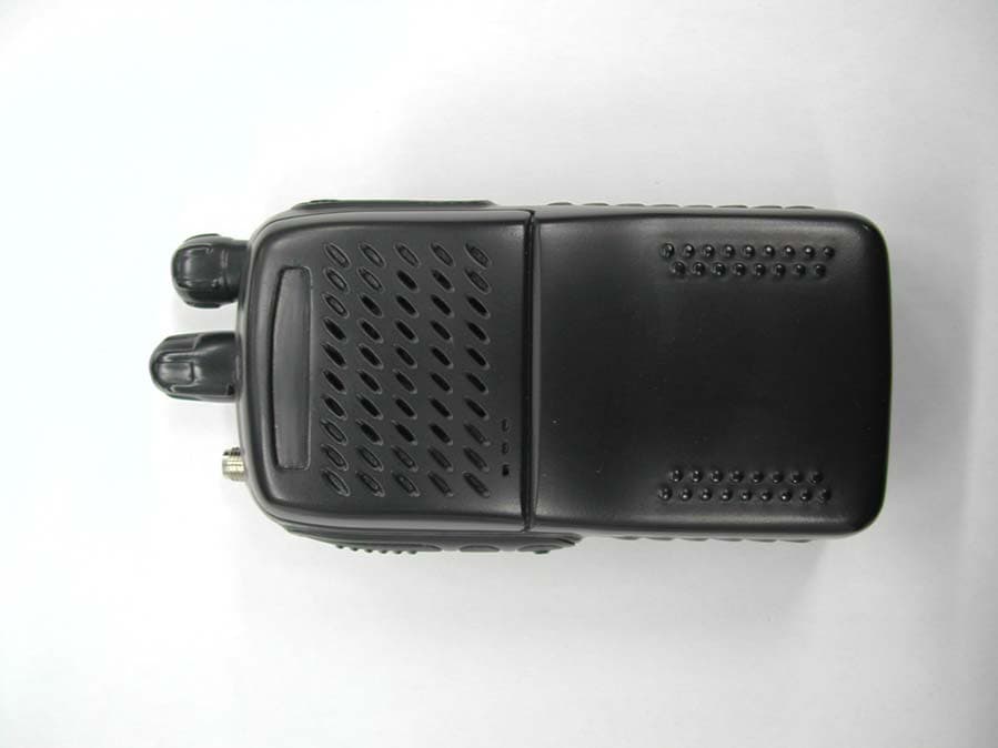
IV9BSHH16V
Dec 30, 2004VHF Transceiver
Equipment Class
TNF - Licensed Non-Broadcast Transmitter Held to Face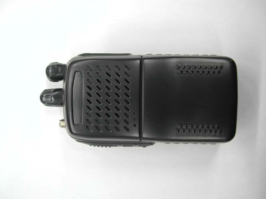
IV9BSHH16U
Dec 30, 2004UHF Transceiver
Equipment Class
TNF - Licensed Non-Broadcast Transmitter Held to Face
IV9FNCU-M45
Sep 27, 200445W UHF RADIO
Equipment Class
TNB - Licensed Non-Broadcast Station Transmitter
IV9FNCU-H45
Sep 20, 2004UHF TRANSCEIVER
Equipment Class
TNB - Licensed Non-Broadcast Station Transmitter