JF6-8702-12Digital Modulated Radio
Alcatel USA Marketing, Inc.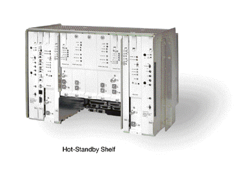
Click to zoom
Application Details
- Equipment Class
- TNB - Licensed Non-Broadcast Station Transmitter
- Date of Grant
- Nov 20, 2005
- Application Purpose
- Original Equipment
- Date of Application
- Sep 27, 2005
- Equipment Note
- Digital Modulated Radio
- Frequency Range
- 2305.00000000 - 2360.00000000
- Company
- Alcatel USA Marketing, Inc.
- Country
- United States
Documents & Files
Document Text
Text extracted from the exhibit documents filed with the FCC. Open a document above to read the original.
Users Manual
EXHIBIT 6. USER’S MANUAL The MDR-8000 series Microwave Digital Radios (see Figure ) consists of: • Solid-state, licensed, digital radios that provide transport for DS1 and E1 in 1.85, 2, 6, 7, 8, 10, and 11 GHz RF bands, DS3 in 2, 6, 7, 8, and 11 GHz RF bands, and OC3 in 6, 7, 8, and 11 GHz RF bands • Solid-state, unlicensed digital radios that provide transport for DS1 and DS3 in the 5 GHz RF frequency band. The following capacities and modulation schemes are available: • MDR-8000 – 2, 4, 8, 12, or 16 North American Standard DS1 channels at either 32 or 128 TCM or 1, 2, or 3 North American Standard DS3 channels with 1, 2, or 3 wayside DS1 channels at 64 QAM • MDR-8000i – 2, 4, 8, 12, or 16 CCITT E1 channels at either 32 or 128 TCM • MDR-8000u – 2, 4, 8, or 16 North American Standard DS1 channels at 32 TCM. SHELF CONFIGURATIONS The MDR-8000 is available in two shelf configurations: hot-standby and CommPak. HOT STANDBY SHELF The MDR-8000 hot-standby shelf is wired hot-standby and can be configured non- standby, where only the A-side is populated, or hot-standby, where both the A- and the B- sides are populated. The hot-standby shelf fits into a standard 19 in. (483 mm) rack and occupies seven vertical rack increments. Up to four fully equipped hot-standby radios can be mounted in a standard 7 ft. rack. The radio is front accessible and can be mounted against a wall or back-to-back against other equipment. COMMPAK RADIO The MDR-8000 CommPak radio is available as a full indoor shelf or outdoor unit in a cabinet. COMMPAK INDOOR SHELF The CommPak indoor shelf is wired and configured non-standby only. The indoor shelf fits into a standard 19 in. (483 mm) rack and occupies four vertical rack increments (7 in.). The radio is front accessible and can be mounted against a wall or back-to-back against other equipment. COMMPAK OUTDOOR UNIT The MDR-8000 outdoor unit consists of the CommPak indoor shelf mounted vertically in a 20 in. high x 7.5 in. wide x 12.5 in. deep enclosure. STANDARD FEATURES Standard features include: • Frequency bands from 1.85 to 11 GHz • Committee of European Post and Telegraph (CEPT)/Federal Communications Commission (FCC) applications • DS1, E1, DS3, and OC3 Traffic capacities • International Telecommunications Union (ITU)/ETSI/FCC compliant • Five configuration options • Upstream management compatibility. • User-friendly Personal Computer (PC) monitor and control • Automatic Transmitter Power Control (ATPC) • Adaptive Time Domain Equalization (TDE) • Extended Link Monitor Channel (ELMC) • MCS-11/Telemetry Byte Oriented Serial (TBOS) Alarm/Control Interface • Two independent PCM audio channels Figure 1 Typical MDR-8000 Series Microwave Digital Radio Table Physical, Environmental, and Electrical Characteristics ITEM CHARACTERISTICS PHYSICAL CHARACTERISTICS Dimensions WIDTH DEPTH HEIGHT Hot-Standby Shelf 483 mm (19 in.) 406.4 mm (16.25 in.) 311.15 mm (12.25 in.) CommPak Indoor Shelf 483 mm (19 in.) 406.4 mm (16.25 in.) 177.8 mm (7.0 in.) Weight (Hot-Standby Terminal)38.6 kg (85 lbs) ENVIRONMENTAL CHARACTERISTICS Ambient Temperature Spec Compliant Operating Without Failure Nonoperating 32° to 122°F (0° to 50°C) - 4° to 158°F (- 20° to 70°C) - 40° to 176°F (- 40° to 80°C) Altitude Operating Nonoperating Relative Humidity Vibration and Shock Duty Cycle -350 to 16500 ft (-100 to 5000 m) -350 to 40000 ft (-100 to 12000 m) 5 to 95 percent (without condensation) Normal Storage and Handling Continuous, unattended COMMON ELECTRICAL CHARACTERISTICS Primary Input Voltage ±20.5 to ±60.0 Vdc RF CHANNEL FREQUENCY (MHZ) MDR-8X02/i-X MDR-8X05u-X MDR-8X06/i/s-X MDR-8X07/i/s-X MDR-8X08/i/s-X MDR-8X10/i/s-X MDR-8X11/i/s-X 1850-2285 5725-5850 5850-7125 7125-7750 7700-8500 10440-10680 10700-11700 XMT OUTPUT POWER (DBM, NOMINAL) XMTR (NO PA) OPTIONAL PA INSTALLED MDR-8X02/i-X MDR-8505u-X MDR-8605u-X MDR-8X06/i/s-X MDR-8X07/i/s-X +14 +15 +14 +14 +14 +30 or +33 +25 or +30 +23 or +29 +23 or +29 or +31 or +33 MDR-8X08/i/s-X MDR-8X10/i/s-X MDR-8X11/i/s-X +14 +15 +15 +28 or +30 +28 or +30 or +32 +23 or +27 or +29 +23 or +27 or +29 Note: XMT Power Referenced at the SMA output of the diplexer filter or the top of the stack for waveguide stacking configurations. Figure 1. Typical MDR-8000 Hot-Standby Shelf Component
External Photos
Exhibit 2 Figure 1 Typical MDR-8000 Series Microwave Digital Radio Figure 1 Typical MDR-8000 Hot-Standby Shelf Component
Internal Photos
EXHIBIT 7. INTERNAL PHOTOS I/O CONDITIONER CIRCUIT SIDE I/O CONDITI0NER SOLDER SIDE TRANSMITTER RF CIRCUIT SIDE TRANSMITTER RF SOLDER SIDE TRANSMITTER BASEBAND CIRCUIT SIDE TRANSMITTER BASEBAND SOLDER SIDE
Internal Photos
EXHIBIT 7. INTERNAL PHOTOS CONT. PA RF SOLDER SIDE PA RF SOLDER SIDE PA BIAS BOARD CIRCUIT SIDE PA BIAS BOARD SOLDER SIDE
Operational Description
EXHIBIT 9. MDR–8000 Operational Description In the transmit direction the MDR–8000 uses a modulation structure where the I and Q baseband signals modulate the in–phase and quadrature phase components of the transmitter. The DS1/E1 I/O interface converts the format of the incoming DS1/E1 data streams to I, Q, data, and clock. The DS1/E1 I/O interface module uses the DS1/E1 signals to generate 32 or 128 trellis code amplitude modulated (TCM) baseband signals The transmitter processes the TCM baseband signals to generate the modulated TCM RF signal. The RF signal is then amplified and applied directly to the antenna branching or further amplified by a solid–state amplifier (optional) and applied to the antenna branching. In the receive direction, the MDR–8000 uses a demodulation conversion structure. The received TCM RF signal is fed into a filter followed by a receiver module. The receiver module directly converts the RF signal to I and Q baseband signals and provides all of the acquisition loops. The receiver also provides countermeasures to dynamic path distortions. Clock and digital data are extracted from the analog channels and passed on to the I/O interface. The digital data is processed by the I/O interface module and converted to a DS1/E1 format. WCS development requirements: Four components need to be developed: Transmitter Receiver Power Amplifier RF filters. The Transmitter, Receiver and Power Amplifier are all modified versions of the PCS band modules. The 6 MHz bandwidth filter is intended for use at sites where other microwave transmitters are co-located and operate at frequencies very close to the MDR-8X02 receiver operating frequency. The filter is designed to provide at least 30 dB of rejection 7 MHz away from the operating frequency. Transmitter: • The main development of the Transmitter is to improve the out-of-band noise floor. • One goal is to increase the frequency flexibility of the current 2GHz Transmitter to accommodate the WCS application. • The transmitter design is based on a phase locked VCO which is a stepping stone to a synthesized transmitter in the future. • The requirements are as follows: • T/L PN: 3EM11962ADAA • PB/RF: 3EM11960ACAA • PBA/RF: 3EM11961ADA • BB ASSY: 3DH03139 • Frequency range: 2305 – 2360 MHz (WCS Band) • RF DC requirements: +/- 5 VDC, +10.5 VDC, +/- 12 VDC • Interface requirement: • Baseband interface: 20 pin, thru hole male connector • I/Q inputs:------- -10dBm • RF detect:------ 500mV +/- 50mV • DC:-------------- +10.5 +/- .2 VDC +5 +/- .1 VDC -5 +/- .1 VDC +12 +/- .2 VDC -12 +/- .2 VDC • Freq Ctrl---------- +3.0 VDC • VVA control------ 0 to 3 VDC • LO interface: 10 pin ribbon connector • LO level: --------- +10 dBm +/- 2 dB • LO monitor: BNC connector • LO level: --------- -10 dBm +/- 2 dB • RF monitor: SMA connector • Level: -------------- 0 dBm +/- 2 dB • RF monitor: SMA connector • Level: ------------- +18 dBm Receivers: • The Receiver effort will be an effort to maximize T/I performance, modifying some baseband filtering and optimizing gain/linearity of the design. The design is based on a phase locked VCO. As with the transmitter, receiver frequency flexibility is required. • The requirements are as follows: • T/L PN: 3EM11964AAAA • PB/RF: 3EM11963ACAA • PBA/RF: 3EM11964ADAA • BB ASSY: 3DH03134AKAH • Frequency range: 2305 – 2360 MHz (WCS Band) • RF DC requirements: +/- 5 VDC, +/- 12 VDC • Interface requirement: • Baseband interface: 20 pin, thru hole male connector • DC:--------------- +5 +/- .1 VDC -5 +/- .1 VDC +12 +/- .2 VDC -12 +/- .2 VDC • Freq Ctrl---------- +3.0 VDC • AFC -------------- 0 to 3 VDC • LO interface: 10 pin ribbon connector • LO level: --------- +10 dBm +/- 2 dB • LO monitor: BNC connector • LO level: --------- -10 dBm +/- 2 dB • RF input: SMA connector • Input Level: ---- -15 to -92 dBm • RF Gain: ----------28 dB max. • NF: -------------- 2.8 dB max. Power Amplifiers: • The Power amplifier will be a slight modification of the Canadian 2GHz. • RF input: SMA connector • Input Level: ---------- -12 dBm • RF Gain: ---------------25 dB max. • RF Output: SMA connector • RF Output Pwr: ------+36 dBm max.
Parts List/Tune Up Info
6-3 6 INITIAL TURNUP 6.1 SECTION INTRODUCTION This section describes the procedures required to turn up the MDR-8000 Microwave Digital Radios after installation. This provisioning part of the section describes provisioning options available with the MDR-8000 software application. Provisioning allows for the definition, editing, and storing of specific functions. The MDR-8000 provides the ability to provision equipment and facili- ties through a series of Windows™-based screens and messages. The Provisioning menu lists equipment and functions which may be provisioned. You should use only those provi- sioning screens that are applicable to your radio. Refer to the Users Guide section and applicable DS1/E1, DS3, or OC3 Initial Turnup section on the attached CD for more infor- mation. 6.2 RECOMMENDED SEQUENCE Perform the following initial turnup procedures in sequence: 1 Install software on PC. Software installed at the factory before delivery should not be overwrit- ten by downloading to the radio controller at initial turnup. Refer to Maintenance section on the attached CD for procedure to upgrade existing software. 2 Establish communication between radio and USI computer. Saving provisioning on disk provides a reference for any future provi- sioning changes. 3 Provision radio. See Figure 6-1. The radio has been properly aligned and tested at the factory before shipment eliminating the need for testing after initial turn-up. The only time testing and/or adjustment is required is after a maintenance action such as removal and replacement procedure and/or constant alarms requiring corrective maintenance action. The completed maintenance action procedure(s) will reference any required test procedure(s). Note Note 6-4 Figure 6-1 Provisioning Sequence LMW-9038-sm 01/23/04 FIG 6-5 DS3 RADIO CONFIG PROVISIONING FIG 6-2 DS1/E1, DS3, OC3 RADIO CONFIG PROVISIONING FIG 6-6 DS3 FACILITIES PROVISIONING FIG 6-3 DS1/E1 RADIO CONFIG PROVISIONING FIG 6-4 DS1/E1 FACILITIES PROVISIONING FIG 6-7 OC3 RADIO CONFIG PROVISIONING FIG 6-8 OC3 FACILITIES PROVISIONING FIG 6-9 DS3, OC3 RADIO WAYSIDE DS1 FACILITIES PROVISIONING FIG 6-13 DS1/E1, DS3, OC3 RADIO ELMC PROVISIONING FIG 6-10 DS1/E1, DS3, OC3 RADIO SERVICE CHANNEL PROVISIONING FIG 6-11 DS1/E1, DS3, OC3 RADIO AUDIO PROVISIONING FIG 6-12 DS1/E1, DS3, OC3 RADIO MCS-11 PROVISIONING FIG 6-14 DS1/E1, DS3, OC3 RADIO ELMC REMOTE TIME-OUT CONSTANT PROVISIONING FIG 6-16 DS1/E1, DS3, OC3 RADIO STATION ALARM NAMES PROVISIONING START END OPTIONAL ENTRY FIG 6-15 DS1/E1, DS3, OC3 RADIO CONTROL NAMES PROVISIONING OPTIONAL ENTRY DS1/E1DS3OC3 6-5 6.3 PROVISIONING RADIO Screen shown is for DS1 Radio. DS3 and OC3 radio configuration pro- visioning is similar. Changes to provisioning do not have to be made in any particular order. Open radio provisioning screens. On main screen, double click on tower icon. Status and alarm screen displays. Click on Provisioning. Check current provisioning and change as required. Figure 6-2 DS1/E1, DS3, OC3 Radio Configuration Provisioning (Sheet 1 of 4) Note ATPC EnabledA&B PA Present RADIO CONFIG: HS Tx/HS RxTERMINAL 6-8 GHz SYSTEM ALARM Visual/AudibleRelays ON/NOStation Alarm 13-16RSL Alarm Enable RSL-Sw EnableEye BER Disable RCV SWITCHING: RADIO TYPE: MDR-8000 DS116 LINES128 TCM OPTIONS: Stat/Prov/WaySideOption Key: SYSTEM ID: TEST1 Disable RADIO LINK ID:ELMC: SELECT DISABLE OR DOUBLE CLICK TO ENABLE (00 DISPLAYS). ENTER 2-DIGIT NUMBER BETWEEN 00 AND 99 AS IDENTIFICATION FOR RADIO RCV/XMT PAIR. USE FOR FREQUENCY COORDINATION IN CONGESTED AREAS THAT HAVE NEARBY TRANSMITTERS AT SAME FREQUENCY WITH SAME MODULATION. ID MUST BE SAME AT BOTH ENDS OF HOP. IF RCV ID DOES NOT MATCH ID RECEIVED FROM FAR-END XMTR, A USI ALARM AND RACK ALARM ARE GENERATED. DISPLAYS NUMBER OF LINES AVAILABLE AS DETERMINED BY CAPACITY KEY. CHANGING NUMBER OF LINES REQUIRES CHANGING CAPACITY KEY. SELECT APPROXIMATE ERROR RATE AT WHICH EYE CLOSURE ALARM ACTIVATES AND SWITCHING OCCURS: EYE BER=1X10 -5 , 1X10 -6 , 1X10 -7 , 1X10 -8 OR SELECT Eye BER Disable TO ACTIVATE ALARMS AT APPROXIMATELY 1X10⁻⁶ WITHOUT RECEIVERS SWITCHING. SELECT A&B PA Present IF SHELF IS EQUIPPED WITH A&B PAs, A OR B PA ONLY IF RACK IS EQUIP- PED WITH ONLY ONE PA, OR NO PA IF SHELF IS NOT EQUIPPED WITH PA. UNEQUIPPED PA ALARMS ARE DISABLED. SELECT Major/Minor TO TRIGGER MAJOR ALARM ON ANY ALARM ON ON-LINE SIDE AND MINOR ALARM ON ANY ALARM ON OFF-LINE SIDE. SELECT Visual/ Audible TO TRIGGER RACK ALARM ON ANY ALARM ON ON-LINE SIDE. DISPLAYS ELMC OPTION KEY TYPE INSTALLED ON CON- TROLLER. STAT (STATUS)/PROV (REMOTE PROVISIONING)/ WAYSIDE (WITH WAYSIDE DS1 MONITORING). NOT PRO- VISIONABLE. CHANGING DISPLAY REQUIRES CHANGING OPTION KEY. SELECT TERMINAL, REPEATER, RING TERMINAL OR RING REPEATER FROM DROP DOWN LIST. SELECT REPEATER IF TRAFFIC AND SERVICE CHANNEL (FOUR RAILS OF X/Y DATA) ARE BEING TRANSPORTED BETWEEN J314 OF BOTH SHELVES. ENABLE OR DISABLE AUTOMATIC POWER CONTROL (ATPC) FUNCTION. SELECT ATPC Disable, ATPC Enabled, OR ATPC with Timeout FROM DROP DOWN LIST. SEE SHEET 2 0F 3 FOR DETAILS. DISPLAYS MODULATION SCHEME. NOT PROVISIONABLE DISPLAYS RADIO TYPE NOT PROVISIONABLE BACKSPACE TO DELETE CURRENT ADDRESS AND ENTER 5-DIGIT REMOTE RACK ADDRESS. SEE FIGURE 6-11 FOR DETAILS. SELECT RSL-Sw Enable TO ENABLE AUTOMATIC RECEIVER SWITCHING BASED ON RSL. WHEN ENABLED, RECEIVER SWITCHES IF: 1. ON-LINE RCV RSL IS BELOW RCV AGC THRESHOLD, AND 2. OFF-LINE RCV RSL IS ABOVE RCV AGC THRESHOLD. SELECT RSL-Sw Disable TO DISABLE AUTOMATIC RECEIVER SWITCHING. LMW-7084 Sheet 1 of 2 02/04/03 SELECT Station Alarm 13-16 TO ENABLE STATION ALARM 13-16 INPUTS TO RELAY INTFC. WHEN EXTERNAL TBOS IS WIRED TO RADIO, SELECT TBOS Display 1-8 TO ENABLE TBOS DRIVERS ON CONTROLLER AND SELECT A TBOS DISPLAY (1-8) TO VIEW. SELECT Relays ON/NO (NORMALLY OPEN-HIGH IMPEDANCE) OR Relays ON/NC (NORMALLY CLOSED- GROUND) ON ALARM FOR ALARM/STATUS OUTPUTS OR Relays OFF. REFER TO RELAY INTERFACE IN THEORY SECTION FOR DETAILS. 6-6 Screen shown is…
Text truncated - open the document above for the full version.
Test Report
EXHIBIT 3 2.983 Supporting Documentation 2.984 RF Power Output 2.985 Modulation Characteristics 2.986 Occupied Bandwidth 2.987 Emissions at Antenna Port 2.988 Field Strength Spurious Radiation 2.989 Frequency Stability 2.983. MDR-8000 FCC Type Acceptance A. Name of Manufacturer Alcatel USA 3400 W. Plano Parkway Plano, TX 75075 B. The equipment for which Type Acceptance is requested is referred to as the MDR-8X02. MDR is an abbreviation for M icrowave Digital Radio. The 8 refers to an Alcatel product numbering scheme that implies the eighth generation of microwave products. The X can either be a 5 or a 7 referring to the modulation scheme implemented. The 5 implies a 32 Trellis Coded Modulation (TCM) scheme while the 7 implies 128 TCM. The last two digits imply the frequency band of the radio. In this case 2 GHz. C. The MDR-8X02 is planned to be a fully supported microwave product with sales exceeding the quantity of one. D. Technical Description 1. FCC ID Emission Designator JF6-8702-16 5M00D7W JF6-8702-12 3M75D7W JF6-8702-8 2M50D7W JF6-8702-4 1M25D7W JF6-8702-2 800KD7W JF6-8502-8 3M75D7W JF6-8502-4 2M50D7W JF6-8502-2 1M25D7W 2. 2305 to 2360 MHz 3. One transmit power option of +33 dBm is provided for the MDR-8X02 WCS radio. The power is measured at the top of the waveguide stack. For operation in the C and D blocks of the WCS band it was necessary to reduce the transmit power by 1 dB due to the increase insertion loss of the 6 MHz narrow band filter. 4. The maximum rated RF power as submitted in FCC Form 731 is 2 Watts MDR-8702-12 Private/Common Carrier Digital Radio Radio Characteristics FCC Identification JF6-8702-12 Frequency Range 2.305-2317.6 GHz and 2347.5-2.360 GHz RF Channel Bandwidth 5.00 MHz Occupied Bandwidth 3.271 MHz Emission Designation 3M75D7W Modulation Type 128 TCM Data Range 18.94 Mb/s Baud Rate 3.03 Mbaud/s Data Efficiency 6.25 bits/Hz Transmit Power +33 dBm (2 Watts) Transmit Frequency Stability 0.005 % (-20 to +50 Degrees C.) Primary Voltage Range 24 – 48 Vdc (positive or negative) Operating Temperature Range 0 to 50 Degrees C Attached Support Documents Equipment Photograph FCCID Label Drawing Defining location of FCCID label 2.984 RF Power Output 2.985 Modulation Characteristics 2.986 Occupied Bandwidth 2.987 Emissions at Antenna Port 2.988 Field Strength of Spurious Radiation 2.989 Frequency Stability 2.990 RF POWER OUTPUT Power output is measured and set at the RF antenna port of the transmitter using an HP 436A Power Meter with an HP 8481 B High Power sensor. The transmit power is set at the desired level by adjusting the Power Amplifier GAIN ADJ at the front of this module. The Power Amplifier has the following characteristics: Alcatel Part Number: 3EM 09037 ADAA Type Design: Solid State DC Power Requirement: +10.5 VDC @ 7.3A -12 VDC @ 100 mA -5 VDC @ 100 mA Gain: 25 dB typical Output Power: +33 dBm transmit power at the RF antenna 2.991 MODULATION CHARACTERISTICS The modulation employed in this equipment is 128 and 32 TCM (Trellis Coded Modulation). This modulation was selected to achieve good BER (bit error rate) performance while maintaining a high spectral efficiency. The TCM signal is similar to a QAM signal, but has been digitally encoded to allow the receiver to correct small noise perturbations. It is generated by direct modulation of the RF carrier and its quadrature frequency component using the I and Q baseband signals. The I and Q baseband signals are fed a modulator IC on the RF Board. The output of the transmit local oscillator is also fed to the modulator IC through a transformer splitter. Each baseband signal (I and Q) is applied to a mixer inside the Modulator IC where it is translated to RF using the In-phase and quadrature components also within the IC. The translated I and Q spectrums are then combined within the same IC to form the suppressed carrier RF spectrum which is subsequently fed into the linear solid state power amplifier. Overhead data is added to the traffic data to carry framing and service channel information. The service channels are used to carry alarm reporting and voice orderwire data. They also provide a channel for microprocessor communication between radio transmitters and receivers. The receiver processor must be able to communicate with the transmit processor for ATPC (automatic transmit power control used to reduce transmit power when not needed) and for indicating possible transmit failure due to total loss of receive signal. Figure 1 shows the typical transmit spectrum characteristics of the modulated signal. FIGURE 1. Typical Spectrum 2.992 OCCUPIED BANDWIDTH Occupied bandwidth was measured at the RF antenna port of the transmitter using an Agilent 4407B spectrum analyzer. This analyzer is equipped to directly measure the 99% power bandwidth of signal. 12 DS1 128 TCM
Test Report
2.983 EMISSIONS AT ANTENNA PORT Emission limits are defined as per Part 27.53. All attenuations are for signals outside of the licensed bandwidth and are referenced to the total RMS transmitter power, measured in a 1 MHz resolution bandwidth. The requirements are defined as follows: 27.53.a.1: Attenuation of frequencies between 2320 and 2345 MHz is at least 80 + 10 LOG (mean output in watts) below the mean output power. For a 2 Watt system this results in an attenuation of 83 db below reference power. 27.53.a.3: Attenuation of frequencies below 2300 MHz or above 2370 MHz is at least 70 + 10 LOG (mean output power in watts) below the mean output power. For a 2 Watt system this results in an attenuation of 73 db below reference power. Attenuation of frequencies between 2300 and 2320 MHz or between 2334 and 2370 MHz that are outside of the licensed channel is at least 43+ 10 LOG (mean output power in watts) below the mean output power. For a 2 Watt system this results in an attenuation of 46 db below reference power. Measurements near the transmitter frequency were made in a 30 kHz resolution bandwidth to provide more accuracy in measuring the spectrum shape. Tones and signals occupying less than a 30 kHz bandwidth will measure the same level as a 1 MHz resolution bandwidth and no adjustment is necessary. Any signal measurement occupying more than a 30 kHz bandwidth must be adjusted to the defined 1 MHz resolution bandwidth. For flat noise this adds 10log (1000/30) = 15 dB to the attenuation requirements. All measurements were made with a transmitter tuned to operate at 2352.5 MHz. Noise level measurements were made at the frequency offset of the nearest channel band edge for each transmitter bandwidth. Transmitter emissions were measured at the antenna port output using HP8566 Spectrum Analyzer. The signal level at the antenna port was adjusted to +33 dBm (normal output). The signal level into the analyzer was attenuated to a reference level of +29 dBm (1 dB below analyzer max input to prevent overload). Measurements were then offset by this reference level. Figure 2 shows a close in view of the modulated spectrum. Figure 3 shows the same modulated spectrum over a wider range. The limits of the nearest channel edge are shown by the dark line. Section 27.53.a.3 specifies an attenuation of 46 + 15 = 61 dB for flat noise. Since the emission measurements do not apply to signals within the licensed channel, the 1 MHz measurement is stopped 500 kHz from the channel edge. For most of the spectrums the emissions still appear as wideband noise and the 15 dB correction applies. For the spectrum shown in Figures 2 and 3 of JF6-8702-16 there is a slight spillover of the transmit signal into the adjacent1 MHz measurement band. This spillover appears as narrow band noise; therefore the 15 dB correction does not apply. Due to the limited dynamic range of the analyzer, it was necessary to create a notch filter to attenuate the transmitter output when measuring attenuations greater than 70 dB. This was done by reversing the output circulator and connecting a second transmit bandpass filter, tuned to the transmitter frequency and terminated in 50 ohms, to the receiver port of the circulator. The circulator passes signals from the transmitter to the second filter. Signals in the passband of the second filter are passed through and absorbed by the termination. The circulator then passes the reflected signals to the attenuator and spectrum analyzer. This forms a notch filter where the rejectband is the passband of the second bandpass filter. The rejectbands of the second filter become the passbands of the notch filter. PA CIRCULATOR TERM XMT FILTER XMT FILTER VAR Atten +29 dBm AGILENT 4407B +33 dBm @ antenna port Connect for notch filter The response of the transmitter output with the notch filter installed and the first transmit bandpass filter removed is included in Figure 4 to show the notch filter effects. The noise floor of the transmitter is attenuated in the reject band of the notch filter. The notch filter has no effect on the transmit signal at frequencies more than +/- 5 MHz from its center. The attenuation of the noise in the rejectband from the flat line response should be added to the noise levels measured at the transmitter output. For example, signals +/- 3 MHz from center are attenuated 10 dB. No adjustments were made to the transmitter output level with the notch filter installed, but the attenuation setting of the analyzer was reduced by 30 dB to increase the signal level above the analyzer noise and allow measurement of the transmitter noise floor. The reference level of the analyzer was also changed by 30 dB to compensate for the reduced attenuation. Figure 5 represents the noise emissions at the nearest band edge of a transmitter operating in the 2305 to 2315 MHz or 2350 to 2360 MHz blocks. Section 27.53.a.1 requires the noise to be attenuated by 83 + 15 = 98 dB. The dark line shows the nearest application of this limit. The notch filter effects are negligible at this band edge. The section 27.53.a.3 limit is lower and farther away. Therefore, its limits are also met. Figure 6 represents the noise emissions at the nearest band edge of a transmitter operating in the 2345 to 2350 MHz block (included only for radios that may operate in this block). Section 27.53.a.1 requires the noise to be attenuated by 83 + 15 = 98 dB. The dark line shows the nearest application of this limit. The section 27.53.a.3 limit is lower and farther away. Therefore, its limits are also met. The asymmetrical noise response is due to the combined effects of the transmit filter and the notch filter. When operating in the 2345 to 2350 MHz block, the transmit filter is centered above the transmitter operating frequency to provide additional rejection of the transmitter idle noise. When operating in the 2315 to 2320 MHz block, the transmit filter is centered below the transmitter operating frequency. The noise emissions …
Text truncated - open the document above for the full version.
Test Report
FIGURE 4. Typical Notch Filter FIGURE 5.
Test Report
FIGURE 7 FIGURE 8 FIGURE 9 2.983 FIELD OF SPURIOUS RADIATION The spectrum emissions of the equipment were measured in an anechoic chamber at a distance of 3 meters. Measurements were made with the receiving antenna mounted both horizontally and vertically. Considering the transmitter as a dipole radiator, the field intensity for a given power at a given distance can be expressed as: E = 10 log ( ( P x 30 x G)/R 2 ) Where: E = field intensity in dBV/m P = transmitter mean output power (+32 dBm = 2 watts) G = dipole antenna gain (1.64) R = radius (3 meters) E = 10 log ( ( 2 x 30 x 1.64)/9 ) = 10.5 dBv/m = 130.5 dBuV/m Part 27.53 specifies that emissions below 2300 MHz and above 2370 MHz must be attenuated from the transmitter power by: A = 70 + 10 LOG (p) = 70 + 10 LOG (2) = 73 dB Therefore, the maximum allowable spurious emissions at 3 meters are: E = 130.5 dBuV/m – 73 dB = 57.5 dBuV/m Measurements were made using a 1 MHz resolution bandwidth and the levels of significant (greater than 35 dBuV/m) spurious emissions were recorded. The significant spurious emissions found are as follows: Horizontial Freq Peak AF Gain Corrected Limit (3m) Delta 72.85 52.8 6.9 2534.749.614.90 121 45.5 7.9 2528.45425.60 145.4 51.5 8.5 25355419.00 148.23 52.1 8.9 253656.920.90 169.6 58.1 9.7 2542.856.914.10 218.2 56.8 11.3 2543.156.913.80 266.9 45.7 12.8 2533.556.923.40 274.9 53.4 13.1 2541.556.915.40 290.85 46.7 13.6 2535.356.921.60 296.4 55.4 14.1 2544.556.912.40 315.1 47.2 14.7 2536.956.920.00 336.07 50.8 15 2540.856.916.10 339.175 54.6 15 2544.656.912.30 345.675 60.1 15.4 2550.556.96.40 363.875 55.6 15.7 2546.356.910.60 395.2 56 16.4 2547.456.99.50 411.95 52.8 16.4 2544.256.912.70 436.32 48.3 16.4 2539.756.917.20 509.12 46.7 18 2539.756.917.20 592.33 50.5 19.8 2545.36014.70 630.7 43.1 21 2539.16020.90 655 48.9 20.8 2544.76015.30 825 47.7 22.3 25456015.00 2036 40.15 21.5 12.549.156010.85 No significant spurious emissions were found above 10 GHz. 2.989 FREQUENCY STABILITY The transmit source that is used is a crystal oscillator operating in the 125 MHz range and multiplied up to the operating frequency. Two sources were tested over a temperature range of 0 to + 50 degrees C and the largest deviation over the specified temperature range was +/- 4 PPM, which is adequate to maintain the transmit spectrum within the desired band of operation as per FCC Part 27.54. Crystal Oscillator Temperature Data -4 -3 -2 -1 0 1 2 3 4 051015 2025 3035 4045 5055 Temperature (Degress C) Parts Per Million The sources were also tested over the range of the DC input voltage and no significant variation in the frequency was observed.
Test Report
2.1051 EMISSIONS AT ANTENNA PORT CONTINUED FIGURE 7 FIGURE 8 FIGURE 9 2.1053 FIELD OF SPURIOUS RADIATION The spectrum emissions of the equipment were measured in an anechoic chamber at a distance of 3 meters. Measurements were made with the receiving antenna mounted both horizontally and vertically. The measurements were made using the “Substitution Method” per TIA-603-C. The dipole equivalent power (P d) was determined using the following formula: Pd(dBm) = Pg(dBm) – cable loss (dB) + antenna gain (dB) Where P g is the generator output power into the substitution antenna. The radiated spurious emissions (dB) was obtained for each spurious frequency using the following equation: 10 log 10 (TX power in watts/0.001) - Pd Measurements were made, using the substitution method, and significant (greater than 75 dB) spurious emissions were recorded. The significant spurious emissions found are as follows: Horizontial Freq(MHZ) Radiated Spurious Emissions (dB) 72.85 70.31 121 58.41 145.4 73.1 148.23 71.4 169.6 70.0 218.2 60.7 266.9 73.7 274.9 66.0 290.85 72.8 296.4 62.0 315.1 74.0 336.07 73.0 339.175 69.5 345.675 62.5 363.875 61.5 395.2 60.7 411.95 64.7 436.32 72.2 509.12 74.2 592.33 67.3 630.7 79.3 655 71.3 825 70.0 2036 62.0 No significant spurious emissions were found above 2.37 GHz with the antenna mounted horizontally. No significant spurious emissions were found with the antenna mounted vertically. 2.1055 FREQUENCY STABILITY The transmit source that is used is a crystal oscillator operating in the 125 MHz range and multiplied up to the operating frequency. Two sources were tested over a temperature …
Text truncated - open the document above for the full version.
Contact Information
Applicant
Alfred Holland(R&D Manager)
Technical Contact
Alcatel USAJake Holland
[email protected](972) 477-8242
3400 W. Plano Parkway · Plano, Texas · United States
Non-Technical Contact
Alcatel USATroy Taylor
[email protected](972) 519-4377
Technical Specifications
| # | Rule Parts | Frequency Range | Power Output | Emission | Tolerance |
|---|---|---|---|---|---|
| 1 | 27 | 2.31 GHz - 2.36 GHz | 2 W | 3M75D7W | 0.0050000000 % |
Other Applications from Alcatel USA Marketing, Inc.
JF6-9558L-D
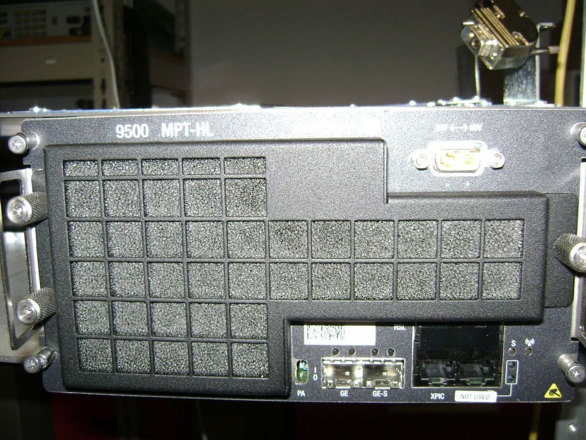
May 28, 20155 GHz rack-mounted point to point transceiver
Equipment Class
DTS - Digital Transmission System
JF6-9558L
May 28, 20155 GHz rack-mounted point to point transceiver
Equipment Class
DTS - Digital Transmission System
JF6-9558HC
Aug 06, 2012Microwave Packet Radio
Equipment Class
DTS - Digital Transmission System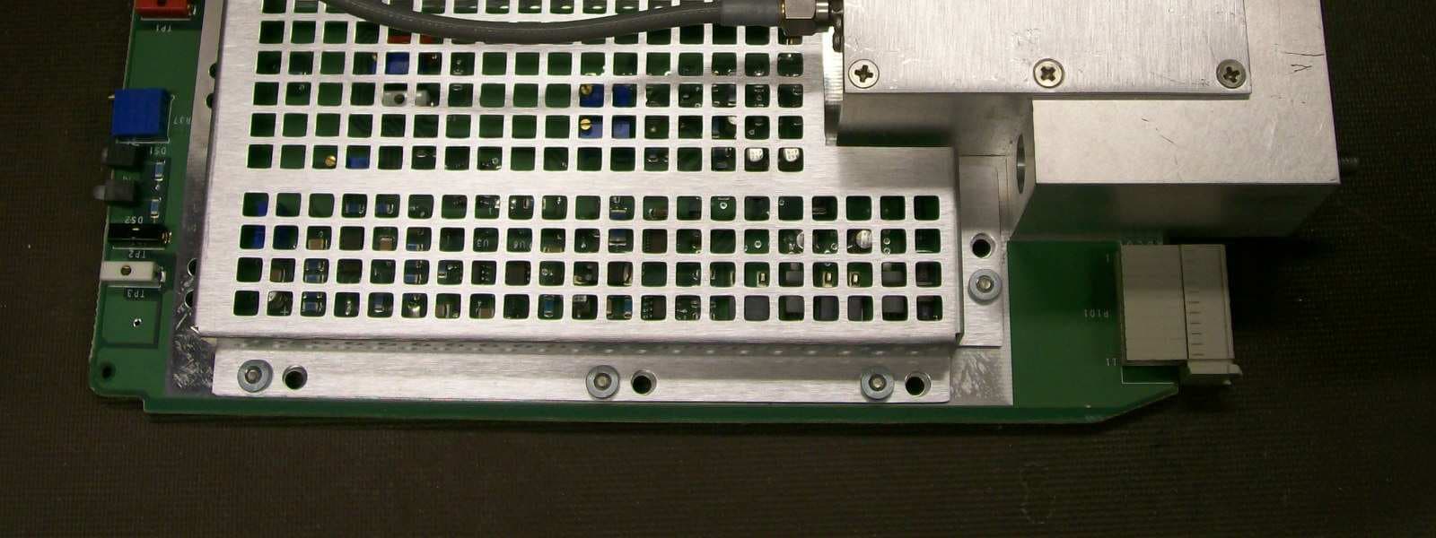
JF6-8702-50
Apr 26, 2010MDR-8000
Equipment Class
TNB - Licensed Non-Broadcast Station Transmitter
JF6-9558H
Jan 03, 2010MPT-HL Packet Terminal
Equipment Class
DTS - Digital Transmission System