K44452501UHF DIGITAL BASE-REPEATER
JVC KENWOOD Corporation
Click to zoom
Application Details
- Equipment Class
- TNB - Licensed Non-Broadcast Station Transmitter
- Date of Grant
- Nov 22, 2015
- Application Purpose
- Original Equipment
- Date of Application
- Nov 22, 2015
- Equipment Note
- UHF DIGITAL BASE-REPEATER
- Frequency Range
- 406.10000000 - 470.00000000
- Company
- JVC KENWOOD Corporation
- Country
- Japan
Documents & Files
Document Text
Text extracted from the exhibit documents filed with the FCC. Open a document above to read the original.
Users Manual
B5A-1121-00 (K) TKR-D710 VHF DIGITAL REPEATER UHF DIGITAL REPEATER INSTRUCTION MANUAL TKR-D810 1 ◆ Do not install the repeater in explosive atmospheres (infl ammable gas, dust particles, metallic powders, grain powders, etc.). ◆ This repeater is intended for use as a fi xed base station with the antenna located outdoors on the rooftop or on an antenna tower. ◆ This repeater is designed for a 13.6 V DC power source! Never use a 24 V DC or higher source to power the repeater. ◆ Use only the supplied DC cord. ◆ Do not remove the ferrite core attached to the DC cord. Doing so may cause interference with radio communications. THANK YOU! We are grateful you purchased this KENWOOD repeater. We believe this easy-to-program repeater will be highly eff ective in your communications system, and will keep personnel operating at peak effi ciency. PRECAUTIONS • Do not expose the unit to rain or moisture; to prevent fi re or electric shock. • Do not open the unit under any circumstances; to avoid risk of electric shock. • Do not expose the unit to long periods of direct sunlight, nor place it close to heating appliances. • Do not place the unit in excessively dusty and/or humid areas, nor on unstable surfaces. • Do not put the plastic bag used for packing of this equipment on the place which reaches a small child's hand. It will become a cause of suffocation if it wears fl atly. • Always switch the transceiver power off before installing optional accessories. • If you detect an abnormal odor or smoke coming from the unit, disconnect the power from the unit immediately. Contact your KENWOOD service center or dealer. NOTICES TO THE USER UNPACKING AND CHECKING EQUIPMENT Note: The following unpacking information is for use by your KENWOOD dealer, an authorized KENWOOD service center, or the factory. Carefully unpack the repeater. We recommend that you identify the items listed in the following table before discarding the packing material. If any items are missing or have been damaged during shipment, fi le a claim with the carrier immediately. ItemPart NumberQuantity Hardware fi xture J21-8559-XX1 Front glass B10-2635-XX1 Name plates B11-1259-XX1 Cushion G13-1801-XX4 Cushion G13-1802-XX4 Foot J02-0475-XX2 Foot J02-0492-XX2 Grommet J59-0302-XX2 Handle K01-0418-XX1 Screws N30-4006-XX2 Screws N35-3006-XX5 DC cord E30-3427-XX1 Lead wire with connector (15 pin) E31-3228-XX1 Fuse F05-1537-XX1 Instruction Manual B5A-1121-XX1 INSTALLATION To install the handles onto the front panel of the repeater, align the handles with the holes on the front panel, then secure the handles using the supplied screws. Please consult your dealer for installing the repeater and antenna. VHF DIGITAL REPEATER/ UHF DIGITAL REPEATER INSTRUCTION MANUAL TKR-D710/ TKR-D810 ◆ Government law prohibits the operation of unlicensed radio transmitters within the territories under government control. ◆ Illegal operation is punishable by fi ne and/or imprisonment. ◆ Refer service to qualifi ed technicians only. One or more of the following statements may be applicable: FCC WARNING This equipment generates or uses radio frequency energy. Changes or modifi cations to this equipment may cause harmful interference unless the modifi cations are expressly approved by the party responsible/JVC KENWOOD. The user could lose the authority to operate this equipment if an unauthorized change or modifi cation is made. INFORMATION TO THE DIGITAL DEVICE USER REQUIRED BY THE FCC This equipment has been tested and found to comply with the limits for a Class B digital device, pursuant to Part 15 of the FCC Rules. These limits are designed to provide reasonable protection against harmful interference in a residential installation. This equipment generates, uses and can generate radio frequency energy and, if not installed and used in accordance with the instructions, may cause harmful interference to radio communications. However, there is no guarantee that the interference will not occur in a particular installation. If this equipment does cause harmful interference to radio or television reception, which can be determined by turning the equipment off and on, the user is encouraged to try to correct the interference by one or more of the following measures: • Reorient or relocate the receiving antenna. • Increase the separation between the equipment and receiver. • Connect the equipment to an outlet on a circuit different from that to which the receiver is connected. • Consult the dealer for technical assistance. Firmware Copyrights The title to and ownership of copyrights for fi rmware embedded in KENWOOD product memories are reserved for JVC KENWOOD Corporation. The AMBE+2 TM voice coding Technology embodied in this product is protected by intellectual property rights including patent rights, copyrights and trade secrets of Digital Voice Systems, Inc. This voice coding Technology is licensed solely for use within this Communications Equipment. The user of this Technology is explicitly prohibited from attempting to extract, remove, decompile, reverse engineer, or disassemble the Object Code, or in any other way convert the Object Code into a human-readable form. U.S. Patent Nos. #6,199,037, #6,912,495, #8,200,497, #7,970,606, and #8,359,197. 2 REPEATER OPERATION Note: ◆ Please consult your dealer for programming the repeater. ◆ After switching the power on, the CH/STATUS display blinks for approximately 30 seconds, until the internal circuit stabilizes. Wait until the display remains lit, before operating. When power is applied to the unit, the POWER indicator lights: Green when using the DC jack. The BUSY indicator lights green while receiving a signal and the TX indicator lights red while transmitting. Rear Panel a TX OUT jack Connect a TX antenna or a duplexer to this receptacle. b CONTROL I/O jack Connect a repeater controller or a remote panel to this DB-25 interface. c REF IN jack This jack is currently not used. d RX IN jack Connect an RX antenna or a duplex…
Text truncated - open the document above for the full version.
Attestation Statements
Oct. 23th 2015 Federal Communications Commission 7435 Oakland Mills Road Columbia, MD 21046 Attn: Reviewing Engineer RE: LETTER OF ATTESTATION FOR MODEL: TKR-D810-K2, FCC ID: K44452501. To whom it may concern: The time division multiple access (TDMA) mode of operation provides two voice paths in a 12.5 kHz channel bandwidth, thus meeting the one voice path per 6.25 kHz of spectrum requirement. This radio also provides a data rate of 9600 bps in a 12.5 kHz channel, thus meeting the minimum data rate of 4800 bps in a 6.25 kHz channel. Please contact me if you require any additional information. Sincerely, Tamaki Shimamura Communications Systems Business Operation 1-16-2, Hakusan, Midori-ku, Yokohama-shi, Kanagawa, 226-8525 Japan
Cover Letter(s)
Oct. 16th 2015 Federal Communications Commission 7435 Oakland Mills Road Columbia, MD 21046 Attn: Reviewing Engineer RE: CONFIDENTIALITY REQUEST FOR MODEL: TKR-D810-K2, FCC ID: K44452501. To whom it may concern: This letter serves as an official request for permanent confidentiality pursuant to 47 CFR Section 0.459 of the Commission Rules. We have requested that the Active Devices, Block Diagram, Circuit Description, Parts List, Schematic Diagrams and Tuning Procedure required to be submitted with this application be withheld from public review. The documents are company proprietary information that could never get into the possession of our competition. Please contact me if you require any additional information. Sincerely, Tamaki Shimamura Communications Systems Business Unit 1-16-2, Hakusan, Midori-ku, Yokohama-shi, Kanagawa, 226-8525 Japan
External Photos
TKR-D810-K2 FCC ID: K44452501 IC: 282F-452501 Front View Rear View TKR-D810-K2 FCC ID: K44452501 IC: 282F-452501 Top View Bottom View TKR-D810-K2 FCC ID: K44452501 IC: 282F-452501 Right View Left View
ID Label/Location Info
SCALE(1:1) SCALE(2:1) 40 25 F 3 4321 A B C D E F 12 E D C B A QTYNo.PART NUMBERPART NAME / NOTEMATERIALFINISH GROUP No. MODEL APPROVEDMATERIALPART NAMESCALE AL EVAPORATION PLATE LINTEC FNS MATT S100 PA-T1 11BL t0.1 MODEL NAME PLATE : CHECKED FINISHDRAWING NUMBERREL. mm SEAL PRINTING TOKA INK UV161 BLACK S STRONG TACKIFIER 00 DESIGNED SHEET No. 1/1 DATE20 - -JIS Z8310 DRWN.DATE2015-10-06 SYMBOLREVISION No.ISSUEDDATE X TKR-D810-K2 FCC ID: K44452501 IC: 282F-452501 Front View (Caution Label) Right View (NAME PLATE)
Internal Photos
TKR-D810-K2 FCC ID: K44452501 IC: 282F-452501 Display Unit A / B Display A Component Side View TKR-D810-K2 FCC ID: K44452501 IC: 282F-452501 Display A Foil Side View Display B Component Side View TKR-D810-K2 FCC ID: K44452501 IC: 282F-452501 Display B Foil Side View Control Unit TKR-D810-K2 FCC ID: K44452501 IC: 282F-452501 Control Component Side View Control Foil Side View TKR-D810-K2 FCC ID: K44452501 IC: 282F-452501 Final A Unit / TX-RX Unit Final A Component Side View TKR-D810-K2 FCC ID: K44452501 IC: 282F-452501 Final A Foil Side View TX-RX Component Side with Shield View TKR-D810-K2 FCC ID: K44452501 IC: 282F-452501 TX-RX Component Side without Shield View TX-RX Component Side without Shield and SUB Unit (RX/TX) View TKR-D810-K2 FCC ID: K44452501 IC: 282F-452501 TX-RX Foil Side with ShieldView TX-RX Foil Side without ShieldView TKR-D810-K2 FCC ID: K44452501 IC: 282F-452501 SUB RX VCO/PLL Component Side View SUB RX VCO/PLL Foil Side View TKR-D810-K2 FCC ID: K44452501 IC: 282F-452501 SUB TX VCO/PLL Component Side View SUB TX VCO/PLL Foil Side View TKR-D810-K2 FCC ID: K44452501 IC: 282F-452501 Final B / C Unit Final B Component Side View Final B Foil Side View Final C Component Side View Final C Foil Side View
RF Exposure Info
Maximum Permissible Exposure (MPE) Evaluation Applicant: JVC KENWOOD Corporation Equipment: UHF DIGITAL BASE-REPEATE R Model No.: TKR-D810-K2 FCC ID: K44452501 IC CN and UPN: 282F-452501 MPE Calculations FCC:1.1310, IC: RSS-102 issus 5 Where: S=Power density (in appropriate units, e.g. mW/cm 2 ) P=Power input to antenna (in appropriate units, e.g., mW) G=Power gain of the antenna in the direction of interest relative to an isotropic radiator R=Distance to the center of radiation of the antenna (appropriate units, e.g., cm) Tx Frequency=406 to 470(MHz) : FCC 406 to 430 , 450 to 470 (MHz) : IC Maximum peak power=(dBm)(=40.5W) Antenna gain=(dBi) S=(mW/cm 2 ) : FCC (mW/cm 2 ) : IC P=(mW) (=Maximum peak power x 120% x Dutycycle50%) G=(numeric) R=(cm) : FCC (cm) : IC Calculated minimum separation distance from antenna :FCC :108.25 (cm) IC :141.34 (cm) 0.27 24300.00 1.64 0.16 141.34 46.07 2.15 108.25 S PG R 4 2 4R PG S
Test Report
Report No :15100016JKA-002 FCC ID:K44452501 IC CN UPN :282F-452501 TRUE FALSE 3 REGULATION :FCC Part 2, 90 RSS-119 Issue 12 JVC KENWOOD CorporationIntertek Japan K.K. Kashima Laboratory URL: http://www.japan.intertek-etlsemko.com 1-16-2, Hakusan, Midori-ku, Yokohama-shi(Anechoic chamber) Kanagawa, 226-8525 Japan 298-6 Sada, Kashima, Ibaraki Tel.: +81 45 939 6254 314-0027 Japan Fax.: +81 45 939 6261 Tel. +81 299 82 8464 (Open area test site) 3-2 Sunayama, Kamisu, Ibaraki 314-0255 Japan Tel. +81 479 40 1097 Equipment typeUHF DIGITAL BASE-REPEATER TrademarkKENWOOD FCC Model(s)TKR-D810-K2 IC Model(s)TKR-D810-K2 Serial No.B5600010 No.2 FCC ID K44452501 IC CN and UPN 282F-452501 Test ResultComplied Report Number15100016JKA-002 Original Issue Date Approved byTested by Hideaki KosemuraKoichi Wagatsuma [Technical Dept. Manager][Engineer] This report is for the exclusive use of Intertek's Client and is provided pursuant to the agreement between Intertek and its Client. Intertek's responsibility and liability are limited to the terms and conditions of the agreement. Intertek assumes no liability to any party, other than to the Client in accordance with the agreement, for any loss, expense or damage occasioned by the use of this report. Only the Client is authorized to permit copying or distribution of this report and then only in its entirety. Any use of the Intertek name or one of its marks for the sale or advertisement of the tested material, product or service must first be approved in writing by Intertek. The observations and test results in this report are relevant only to the sample tested. This report by itself does not imply that the material, product, or service is or has ever been under an Intertek certification program. Applicant TEST REPORT Testing Laboratory November 05, 2015 Intertek Japan K.K.Page 1 of 56 FJP-TE031 Ver.1.0 Effective Date:January 4, 2011 Report No :15100016JKA-002 FCC ID:K44452501 IC CN UPN :282F-452501 In Accordance with FCC Rules and Regulations, Volume II, Part 2 and 90 Sub-part 2.1033 Applicant and Manufacture Information APPLICANT Company:JVC KENWOOD Corporation Address:1-16-2, Hakusan, Midori-ku, Yokohama-sh i Kanagawa, 226-8525 Japan Contact Person:Tamaki Shimamura Manager, Communications Systems Business Unit MANUFACTURER Company:JVC KENWOOD Corporation Address:1-16-2, Hakusan, Midori-ku, Yokohama-sh i Kanagawa, 226-8525 Japan (c)(2) FCC ID FCC ID:K44452501 Model number:TKR-D810-K2 Serial number:B5600010 No.2 Instruction Manual (S) Instruction manual(s):Please refer to attached Exhibits F Type of Emission Emission Designation :16K0F3E 16K0F3E is IC Only 11K0F3E 7K60FXD / 7K60FXE Frequency range Frequency Range:FCC: 406.1 to 470 MHz IC: 406.1 to 430 MHz and 450 to 470 MHz Power Rating Output Power:5 to 40 W Type:Continuously Variable Maximum Power Rating Output Power:40W Collector Current, A:13.0 A Maximum Collector Voltage, Vdc :13.6 Vdc Supply Voltage, Vdc:13.6 Vdc Other Information Number of Channel:30 channels Maximum Deviation:± 5 kHz (16K0F3E), ± 2.5 kHz (11K0F3E) Frequency Stability:0.5 ppm : Antenna Impedance:50 Ω Norminal Note including final transistor or solid-state device Voltages & currents in all elements in final RF stage, Intertek Japan K.K.Page 2 of 56 FJP-TE031 Ver.1.0 Effective Date:January 4, 2011 Report No :15100016JKA-002 FCC ID:K44452501 IC CN UPN :282F-452501 TABLE OF CONTENTS Page SECTION 1. GENERAL INFORMATION4 SECTION 2. SUMMARY OF TEST RESULT5 SECTION 3. TEST AND MEASUREMENT DATA6 SECTION 4. INFORMATION ABOUT EUT AND SUPPORT EQUIPMENT(S)7 SECTION 5. SUPPORT EQUIPMENT8 SECTION 6. USED CABLE(S)9 SECTION 7. TEST CONFIGURATION10 SECTION 8. OPERATING CONDITION11 SECTION 9. MEASUREMENT UNCERTAINTY12 SECTION 10. TEST DATA 10.1 Carrier Output Power (Conducted)13 10.2 Unwanted Emissions (Transmitter Conducted)16 10.3 Field Strength of Spurious Radiation19 10.4 Emission Masks (Occupied Bandwidth)23 10.5 Transient Frequency Behavior30 10.6 Audio Frequency Response / Audio Low Pass Filter (Voice Input)35 10.7 Modulation Limiting39 10.8 Frequency Stability (Temperature Variation)43 10.9 Frequency Stability (Voltage Variation)46 10.10 Receiver Spurious Emissions(Radiated)48 10.11 Necessary Bandwidth and Emission Bandwidth52 10.1299% Occupied Bandwidth53 APPENDIXPHOTOGRAPHS Intertek Japan K.K.Page 3 of 56 FJP-TE031 Ver.1.0 Effective Date:January 4, 2011 Report No :15100016JKA-002 FCC ID:K44452501 IC CN UPN :282F-452501 SECTION 1. GENERAL INFORMATION TEST PERFORMED LocationKashima No.1 Test Site and No.12 Test Site EUT Received Date of Testto Standard AppliedFCC Part 2, 90 RSS-119 Issue 12 Measurement Method Deviation from Standard(s)Not applicable QUALIFICATIONS OF TESTING LABORATORY(Kashima Lab.) ACCREDITATIONSCOPELAB. CODERemarks VLACEMC TestingVLAC-008-1JAPAN BSMIEMC TestingSL2-IN-E-6008TAIWAN FILING VCCIEMC TestingA-0126JAPAN FCCEMC TestingJP0008 ICEMC TestingIC-2042K-3, IC-2042Q-12CANADA CB-SchemeEMC TestingTL222IECEE ABBREVIATIONS EUTDoC AMNISN LISNQ-P AMPAVG ATTPK ANTCal BBAN/A DIPLCD AEAssociated Equipment4LEVEL FSK 4LEVEL Frequency Shift Key GMSKCW ID FMC4FM PTTPush to TalkAFC Revision Summary Declaration of Conformity Not applicable or Not availableBroadband Antenna October 10, 2015November 04, 2015 Attenuator AntennaCalibration Peak ANSI/TIA-603-D-2010 / RSS-119 Issue 12(2015), RSS-Gen Issue 4(2014) Impedance Stabilization Network Continuously Repeating bit stream October 01, 2015 Average Line Impedance Stabilization Network Equipment Under Test Artificial Mains Network Quasi-peak Amplifier Automatic frequency control Dipole AntennaLiquid-Crystal Display Gaussian Maximum Shift Key Frequency ModulationConstant envelope 4 Level FM Description of ChangesRevised DateSection Intertek Japan K.K.Page 4 of 56 FJP-TE031 Ver.1.0 Effective Date:January 4, 2011 Report No :15100016JKA-002 FCC ID:K44452501 IC CN UPN :282F-452501 SECTION 2. SUMMARY OF TEST RESULT FCCICTEST ITEMRESULTSComments Part2Part90RSS-119 2.1046-5.4Carrier Output Power (Conducted…
Text truncated - open the document above for the full version.
Test Setup Photos
Report No :15100016JKA-002 FCC ID:K44452501 IC CN UPN :282F-452501 APPENDIX Intertek Japan K.K.Page 1 of 11 FJP-TE031 Ver.1.0 Effective Date:January 4, 2011 Report No :15100016JKA-002 FCC ID:K44452501 IC CN UPN :282F-452501 PHOTOGRAPHS OF MEASUREMENT SET-UP 10.1 Carrier Output Power (Conducted) Intertek Japan K.K.Page 2 of 11 FJP-TE031 Ver.1.0 Effective Date:January 4, 2011 Report No :15100016JKA-002 FCC ID:K44452501 IC CN UPN :282F-452501 10.2 Unwanted Emission (Conducted Spurious) Intertek Japan K.K.Page 3 of 11 FJP-TE031 Ver.1.0 Effective Date:January 4, 2011 Report No :15100016JKA-002 FCC ID:K44452501 IC CN UPN :282F-452501 10.3 Field Stren gth of Spurious Radiation : Front view 10.3 Field Strength of Spurious Radiation : Rear view Intertek Japan K.K.Page 4 of 11 FJP-TE031 Ver.1.0 Effective Date:January 4, 2011 Report No :15100016JKA-002 FCC ID:K44452501 IC CN UPN :282F-452501 10.4 Emission Mask s Intertek Japan K.K.Page 5 of 11 FJP-TE031 Ver.1.0 Effective Date:January 4, 2011 Report No :15100016JKA-002 FCC ID:K44452501 IC CN UPN :282F-452501 10.5 Transient Fre quency Behavior Intertek Japan K.K.Page 6 of 11 FJP-TE031 Ver.1.0 Effective Date:January 4, 2011 Report No :15100016JKA-002 FCC ID:K44452501 IC CN UPN :282F-452501 10.6 Audio Fre quency Response Intertek Japan K.K.Page 7 of 11 FJP-TE031 Ver.1.0 Effective Date:January 4, 2011 Report No :15100016JKA-002 FCC ID:K44452501 IC CN UPN :282F-452501 10.7 Modulation Limitin g Intertek Japan K.K.Page 8 of 11 FJP-TE031 Ver.1.0 Effective Date:January 4, 2011 Report No :15100016JKA-002 FCC ID:K44452501 IC CN UPN :282F-452501 10.8, 10.9 Fre quency Stability : Outer view 10.8, 10.9 Frequency Stability : Inner view Intertek Japan K.K.Page 9 of 11 FJP-TE031 Ver.1.0 Effective Date:January 4, 2011 Report No :15100016JKA-002 FCC ID:K44452501 IC CN UPN :282F-452501 10.10 Receiver S purious Emission (Radiated) : Front view 10.10 Receiver Spurious Emission (Radiated) : Rear view Intertek Japan K.K.Page 10 of 11 FJP-TE031 Ver.1.0 Effective Date:January 4, 2011 Report No :15100016JKA-002 FCC ID:K44452501 IC CN UPN :282F-452501 10.12 99% Occu pied Bandwidth Intertek Japan K.K.Page 11 of 11 FJP-TE031 Ver.1.0 Effective Date:January 4, 2011
Contact Information
Applicant
Kazuyoshi Akaike(Manager)
Test Firm
Intertek Japan K.K.(Kashima Laboratory)Junichi Okada
Technical Specifications
| # | Rule Parts | Frequency Range | Power Output | Emission | Tolerance |
|---|---|---|---|---|---|
| 3 | 9 | 406.1 MHz - 470 MHz | 40 W | 7K60FXE | 0.5 ppm |
Other Applications from JVC KENWOOD Corporation
K44524000
Jan 23, 2026144/220/430MHz TRIBANDER
Equipment Class
CSR - Scanning Receiver
K44520000
Sep 05, 2024MULTIBAND DIGITAL TRANSCEIVER
Equipment Class
TNB - Licensed Non-Broadcast Station Transmitter
K44521000
Nov 08, 2023144/220/430MHz TRIBANDER
Equipment Class
DSS - Part 15 Spread Spectrum Transmitter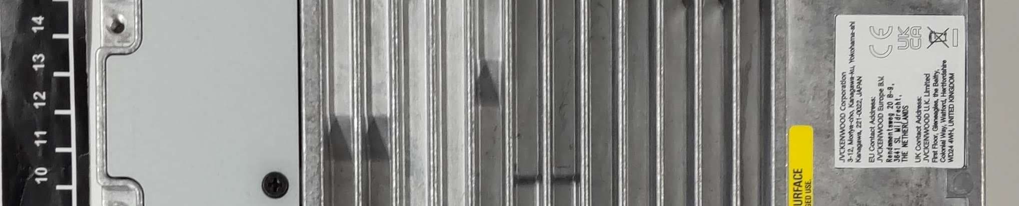
K44513201
May 18, 2023UHF REPEATER
Equipment Class
TNB - Licensed Non-Broadcast Station Transmitter
K44501001
May 25, 2021VHF TRANSCEIVER
Equipment Class
TNF - Licensed Non-Broadcast Transmitter Held to Face