K6610584720HANDHELD TRANSCEIVER
Yaesu Musen Co., Ltd.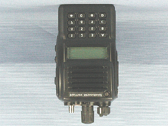
Click to zoom
Application Details
- Equipment Class
- TNF - Licensed Non-Broadcast Transmitter Held to Face
- Date of Grant
- Dec 27, 2004
- Application Purpose
- Original Equipment
- Date of Application
- Dec 27, 2004
- Equipment Note
- HANDHELD TRANSCEIVER
- Frequency Range
- 450.00000000 - 512.00000000
- Company
- Yaesu Musen Co., Ltd.
- Country
- Japan
Documents & Files
Document Text
Text extracted from the exhibit documents filed with the FCC. Open a document above to read the original.
Users Manual
FCC ID: K6610584720 IC ID: 511B-10584720 Operating Manual 1/7 Vertex Standard Co., Ltd. VX-820/870 series Operating Manual SAFETY TRANING INFORMATION This Radio has been tested and complies with the Federal Communications Commission (FCC) RF exposure limits for Occupational Use/Controlled exposure environment. In addition, it complies with the following Standards and Guidelines: - FCC 96-326, Guidelines for Evaluating the Environmental Effects of Radio-Frequency Radiation. - FCC OET Bulletin 65 Edition 97-01 (1997) Supplement C, Evaluating Compliance with FCC Guidelines for Human Exposure to Radio Frequency Electromagnetic Fields. - ANSI/IEEE C95.1-1992, IEEE Standard for Safety Levels with Respect to Human Exposure to Radio Frequency Electromagnetic Fields, 3kHz to 300 GHz. - ANSI/IEEE C95.3-1992, IEEE Recommended Practice for the Measurement of Potentially Hazardous Electromagnetic Fields-RF and Microwave. WARNING: This radio generates RF electromagnetic energy during transmit mode. This radio is designed for and classified as Occupational Use Only, meaning it must be used only during the course of employment by individuals aware of the hazards, and the ways to minimize such hazards. This radio is not intended for use by the General Population in an uncontrolled environment. CAUTION: To ensure that your expose to RF electromagnetic energy is within the FCC allowable limits for occupational use, always adhere to the following guidelines: - This radio is NOT approved for use by the general population in an uncontrolled environment. This radio is restricted to occupational use, work related operations only where the radio operator must have the knowledge to control its RF exposure conditions. - When transmitting, hold the radio in a vertical position with its microphone 1 to 2 inches (2.5 to 5 cm) away from your mouth and keep the antenna at least 1 inch (2.5cm) away from your head and body. - The radio must be used with a maximum operating duty cycle not exceeding 50 %, in typical Push-to-Talk (PTT) configurations. DO NOT transmit for more than 50 % of total radio use time (50 % duty cycle). Transmitting more than 50 % of the time can cause FCC RF exposure compliance requirements to be exceeded. The radio is transmitting when the red LED on the top of the radio is illuminated. You can FCC ID: K6610584720 IC ID: 511B-10584720 Operating Manual 2/7 Vertex Standard Co., Ltd. cause the radio to transmit by pressing the PTT button. - DO NOT transmit when the radio is used in Body Worn configuration with the following accessory: belt-clip. It must be used ONLY for (1) there is a 4 cm distance from the body during transmitting, (2) monitoring purposes, using the speaker only and (3) for carrying purposes. - Always use VERTEX STANDARD authorized accessories. The information listed above provides the user with the information needed to make him or her aware of RF exposure, and what to do to assure that this radio operates with the FCC RF exposure limits of this radio. Electromagnetic Interference/Compatibility During transmissions, this radio generates RF energy that can possibly cause interference with other devices or systems. To avoid such interference, turn off the radio in areas where signs are posted to do so. Do not operate the transmitter in areas that are sensitive to electromagnetic radiation such as hospitals, health care facilities, aircraft, and blasting sites. FCC ID: K6610584720 IC ID: 511B-10584720 Operating Manual 3/7 Vertex Standard Co., Ltd. 1,Controls & Connectors LED Indicator Glows Green: Scan active Blinks Green: Busy Channel (or SQL off) Glows Red: Transmit Blinks Red: Battery Voltage is low Antenna Jack PTT (Push to Talk) Switch Monitor Button Lamp Button CH (Channel) Selector VOL/PWR Knob LCD (without VX-821/871 version) SEL KEY (TOP) MIC/SP Jack (External MIC/SP) Speaker Main Microphone Battery Pack Latch 16-Button DTMF Keypad (VX-829/879 version only) 4-Button DTMF Keypad (VX-824/874 version only) FCC ID: K6610584720 IC ID: 511B-10584720 Operating Manual 4/7 Vertex Standard Co., Ltd. 2,Before You Begin Battery Pack Installation and Removal To install the battery, hold the transceiver with your left hand, so your palm is over the speaker and your thumb is on the top of the belt clip. Insert the battery pack into the battery compartment on the back of the radio while tilting the Belt Clip outward, then close the Battery Pack Latch until it locks in place with a “Click.” To remove the battery, turn the radio off and remove any protective cases. Open the Battery Pack latch on the bottom of the radio, then slide the battery downward and out from the radio while unfolding the Belt Clip. Caution!: Do not attempt to open any of the rechargeable Li-ion packs, as they could explode if accidentally short-circuited. Low Battery Indication As the battery discharges during use, the voltage gradually becomes lower. When the battery voltage reaches 6.0 volts, substitute a freshly charged battery and recharge the depleted pack. The TX/BUSY indicator on the top of the radio will blink red when the battery voltage is low. Avoid recharging Li-ion batteries often with little use between charges, as this can degrade the charge capacity. We recommend that you carry an extra, fully charged pack with you so the operational battery may be used until depletion (this “deep cycling” technique promotes better long-term battery capacity). FCC ID: K6610584720 IC ID: 511B-10584720 Operating Manual 5/7 Vertex Standard Co., Ltd. 3,Operation Preliminary Steps Install a charged battery pack onto the transceiver, as described previously. Screw the supplied antenna onto the Antenna jack. Never attempt to operate this transceiver without an antenna connected. If you have a Speaker/Microphone, we recommend that it not be connected until you are familiar with the basic operation of the VX-820/870. Operation Quick Start To turn the top panel’s VOL/PWR knob clockwise to turn on the radio on. Pul…
Text truncated - open the document above for the full version.
External Photos
FCC ID: K6610584720 IC ID: 511B-10584720 Vertex Standard Co., Ltd. Front view (VX-829/VX-879) Front view (VX-824/VX-874) FCC ID: K6610584720 IC ID: 511B-10584720 Vertex Standard Co., Ltd. Front view (VX-821/VX-871) Rear view FCC ID: K6610584720 IC ID: 511B-10584720 Vertex Standard Co., Ltd. Left side Right side FCC ID: K6610584720 IC ID: 511B-10584720 Vertex Standard Co., Ltd. To p Bottom
ID Label/Location Info
VX-820/870 (UHF) seriesVX-820/870 (UHF) series LABEL DRAWINGLABEL DRAWING Vertex Standard Co., Ltd.Vertex Standard Co., Ltd. ID / Part 15.19 and CAUTION drawings ID drawing Part 15.19 and CAUTION drawings Label location VX-821-G7-5 FCC ID: K6610584720 IC: 511B-10584720 4909959000000 ! ! Device restricted to occupational use to satisfy FCC RF exposure compliance. See owner's manual for specific operating requirement CAUTION This device complies with part 15 of the FCC Rules. Operation is subject to the condition that this device does not cause harmful interference. VERTEX STANDARD CO., LTD. MADE IN JAPAN SER NO. 00000000 VX-824-G7-5 FCC ID: K6610584720 IC: 511B-10584720 4909959000000 VERTEX STANDARD CO., LTD. MADE IN JAPAN SER NO. 00000000 VX-829-G7-5 FCC ID: K6610584720 IC: 511B-10584720 4909959000000 VERTEX STANDARD CO., LTD. MADE IN JAPAN SER NO. 00000000 VX-871-G7-5 FCC ID: K6610584720 IC: 511B-10584720 4909959000000 VERTEX STANDARD CO., LTD. MADE IN JAPAN SER NO. 00000000 VX-874-G7-5 FCC ID: K6610584720 IC: 511B-10584720 4909959000000 VERTEX STANDARD CO., LTD. MADE IN JAPAN SER NO. 00000000 VX-879-G7-5 FCC ID: K6610584720 IC: 511B-10584720 4909959000000 VERTEX STANDARD CO., LTD. MADE IN JAPAN SER NO. 00000000
Internal Photos
FCC ID: K6610584720 IC ID: 511B-10584720 Vertex Standard Co., Ltd. Inside view Chassis with PWB FCC ID: K6610584720 IC ID: 511B-10584720 Vertex Standard Co., Ltd. Side-A of MAIN-UNIT Side-B of MAIN-UNIT with shield case FCC ID: K6610584720 IC ID: 511B-10584720 Vertex Standard Co., Ltd. Side-B of MAIN-UNIT without shield case Front panel with PWB FCC ID: K6610584720 IC ID: 511B-10584720 Vertex Standard Co., Ltd. Side-A of DISPLAY-UNIT with LCD Side-A of DISPLAY-UNIT without LCD FCC ID: K6610584720 IC ID: 511B-10584720 Vertex Standard Co., Ltd. Side-B of DISPLAY-UNIT Front of LCD (for VX-824/829/VX-874/879) FCC ID: K6610584720 IC ID: 511B-10584720 Vertex Standard Co., Ltd. Back of LCD (for VX-824/829/VX-874/879) Inside front panel (for VX-829/VX-879) FCC ID: K6610584720 IC ID: 511B-10584720 Vertex Standard Co., Ltd. Inside front panel (for VX-824/VX-874) Inside front panel (for VX-821/VX-871) FCC ID: K6610584720 IC ID: 511B-10584720 Vertex Standard Co., Ltd. Inside of chassis
Operational Description
FCC ID: K6610584720 IC ID: 511B-10584720 Circuit Description 1/3 Vertex Standard Co., Ltd. VX-820/870 (UHF) series Circuit Description 1. Circuit Configuration by Frequency The receiver is a double-conversion superheterodyne with a first intermediate frequency (IF) of 50.85MHz and a second IF of 450kHz. Incoming signal from the antenna is mixed with the local signal from the VCO/PLL to produce the first IF of 50.85MHz. This is then mixed with the 50.4MHz second local oscillator output to produce the 450kHz second IF. This is detected to give the demodulated signal. The transmit signal frequency is generated by the PLL VCO, and modulated by the signal from the microphone. It is then amplified and sent to the antenna. 2. Receiver System 2-1. Front-end RF amplifier Incoming RF signal from the antenna is delivered to the RF Unit and passes through Low- pass filer, antenna switching diode, high pass filter and removed undesired frequencies by varactor diode (tuned band-pass filer). The passed signal is amplified in Q1021 and moreover cuts an image frequency with the tuned band pass filter and comes into the 1st mixer. 2-2. First Mixer The 1st mixer consists of the Q1034, T1001, T1002 and T1003. Buffered output from the VCO is amplified by Q1032 to provide a pure first local signal between 399.15 and 461.15MHz for injection to the first mixer. The IF signal then passes through monolithic crystal filters XF1001(±5.5 kHz BW) to strip away all but the desired signal. 2-3. IF Amplifier The first IF signal is amplified by Q1056. The amplified first IF signal is applied to FM IF subsystem IC Q1065 which contains the second mixer, second local oscillator, limiter amplifier, noise amplifier, and S-meter amplifier. The signal from reference oscillator X1003 becomes 3 times of frequencies in Q1065, it is mixed with the IF signal and becomes 450KHz. The second IF then passes through the ceramic filter CF1001 (wide channels), CF1002 (narrow channels) to strip away unwanted mixer products, and is applied to the limiter amplifier in Q1065, which removes amplitude variations in the 450kHz IF, before detection of the speech by the ceramic discriminator CD1001. 2-4. Audio amplifier Detected signal from Q1065 is inputted to Q1031 and is output through the band path filter inside Q1031. In the case an optional unit is installed, the Q1078 is made OFF and the AF signal from Q1031 goes the optional unit. In the case an optional unit is not installed, Q1078 is made ON and the signal goes through Q1078. The signal then goes through de-emphasis part and expander Q1022. When the function of expander is off, the signal will be bypassed by Q1014. The output signal of expander (or a signal from de-emphasis) goes through AF mute switch Q1083 and amplified by Q1082. The signal goes to Q1029, and the output from Q1029 is amplified with AF power amplifier Q2017 after passing AF volume Q1020. The output of Q2017 drives a speaker (it chooses the external SP or internal SP in external terminal, SELECT) 2-5. Squelch Circuit There are 13 levels of squelch setting from 0 to 12. The level 0 means open the squelch. The level 1 means the threshold setting level and level 11 means tight squelch. From 2 to 10 is established in the middle of threshold and tight. The bigger figure is nearer the tight setting. The level 12 becomes setting of carrier squelch. 2-5-1. Noise Squelch Noise squelch circuit is composed of the band path filter of Q1065, noise amplifier Q1069, FCC ID: K6610584720 IC ID: 511B-10584720 Circuit Description 2/3 Vertex Standard Co., Ltd. and noise detector D1049, D1050. When a carrier isn't received, the noise ingredient which goes out of the demodulator Q1065 is amplified in Q1069 through the band path filter Q1065, is detected to DC voltage with D1049, D1050 and is inputted to 16pin (the A/D port) of the Q1067 (CPU). When a carrier is received, the DC voltage becomes low because the noise is compressed. When the detected voltage to CPU is high, the CPU stops AF output with Q1078 "OFF" by making the 59pin (CPU) "L" level. When the detection voltage is low, the CPU makes Q1078 ON with making 59pin "H" and the AF signal is output. 2-5-2. Carrier Squelch The CPU (15pin: A/D port) detect RSSI voltage output from Q1065 12 pin, and controls AF output. The RSSI output voltage changes according to the signal strength of carrier. The stronger signal makes the RSSI voltage to be higher voltage. The process of the AF signal control is same as Noise Squelch The shipping data is adjusted 3dB higher than squelch tight sensitivity. 3. Transmitter System 3-1. Mic Amplifier The AF signal from internal microphone J2002 21pin or external microphone J2002 6pin is amplified with microphone amplifier Q2014, after microphone selection switch Q2015, and passes microphone gain volume Q1020. The AF signal which was controlled in the correct gain passes compandor Q1022. When not using a compandor, with the control from the CPU, it passes in the compandor circuit inside of Q1022 and it is output and it passes a pre-emphasis circuit. Q1078 becomes OFF when an option unit is attached and the AF signal from Q1022 goes via the option unit. When an option unit isn't attached, Q1078 becomes ON, the signal passes Q1078 and is input to the pre-emphasis amplifier Q1031. The signal passed limiter and splatter filter of Q1031 is adjusted by maximum deviation adjustment volume Q1020. The adjusted low frequency signal ingredient is amplified by Q1075, added modulation terminal of TCXO (X1003), the FM modulation is made by reference oscillator. The high frequency signal ingredient is amplified Q1075, and adjusted the level by volume Q1020 to make frequency balance between low frequency. After that, it is made FM modulation to transmit carrier by the modulator D1030 of VCO. 3-2. Drive and Final amplifier The modulated signal from the VCO Q1051 is buffered by Q1040 and amplified by Q1032. Then the signal is buffered by Q1027 for the final amplifier driver Q1024…
Text truncated - open the document above for the full version.
Parts List/Tune Up Info
Page 1/3 FCC ID: K6610584720 IC ID: 511B-10584720 VX-820/VX-870 (UHF) seriesComponent Application Address Device name DescriptionApplication [MAIN-UNIT] D 1001 DiodePTZ TE25 15AProtection D 1005 Diode1SS400GProtection D 1006 Diode1SS400GProtection D 1011 DiodeHVU131ANT SW D 1012 DiodeHVU131ANT SW D 1013 Diode1SV331BPF Tune D 1015 Diode1SV331BPF Tune D 1017 Diode1SS400GProtection D 1018 Diode1SS400GRX RF AMP Protection D 1020 Diode1SV331BPF Tune D 1022 Diode1SV331BPF Tune D 1023 DiodeDAN222TX/RX SW D 1024 Diode1SS400GRipple Filter D 1025 DiodeDA221Noise Filter D 1026 DiodeDA221Limiter D 1029 Not use D 1030 DiodeHVC383BModulator D 1032 Diode1SS400Ripple Filter D 1033 DiodeHVC362TRFTX VCO D 1034 DiodeHVC362TRFTX VCO D 1035 DiodeHVC362TRFTX VCO D 1036 DiodeHVC383BRX VCO D 1037 DiodeHVC383BRX VCO D 1038 DiodeHVC383BRX VCO D 1039 DiodeHVC362TRFTX VCO D 1040 DiodeHVC383BRX VCO D 1041 Diode1SS400GReverse Protection D 1042 DiodeDA221Limiter D 1043 DiodeDA221RESET DET D 1044 Zener Diode HZU5ALLProtection D 1046 DiodeDAN222W/N SW D 1047 Diode1SS400GSpeed Up D 1048 DiodeDAN222W/N SW D 1049 DiodeDA221Detector D 1050 DiodeDA221Detector D 1051 Diode1SS400GDetector D 1052 Zener Diode UDZS TE-17 3.9BProtection Q 1002 Transistor XP1501TX 5V Regulator Q 1003 Transistor CPH6102TX 5V Regulator Q 1004 Transistor DTC144EESW Q 1005 ICTAR5S505V Regulator Q 1006 Transistor UMD5N TRSW Q 1010 Transistor DTC114TESW Q 1014 ICCD4053BPWRSelector Q 1017 Transistor DTC144EESW Q 1018 Transistor DTC144EESW Q 1019 FET2SK3476TX PA Q 1020 ICM62364FP 600DLevel Control Q 1021 Transistor HSG2001VFRX RF AMP Q 1022 ICLA8630MCompander / Expander Q 1024 FET2SK3475TX Drive AMP Q 1025 Transistor DTC144EEPo Off SW Q 1027 Transistor 2SC3357-T2TX Pre Drive AMP Q 1028 ICBD6111FV-E2-5V Regulator Q 1029 ICTC4W53FUSelector Q 1030 ICNJM2130FVCV Control Q 1031 ICAK2345AF Base-Band Q 1032 Transistor 2SC5226-4Buffer AMP Q 1033 Transistor DTC144EEP_SAVE SW Q 1034 ICSPM5001RX 1st Mixer Q 1035 Transistor 2SA1774 RRipple Filter Q 1036 Transistor DTA144EEP_SAVE SW Vertex Standard Co., Ltd. Page 2/3 FCC ID: K6610584720 IC ID: 511B-10584720 VX-820/VX-870 (UHF) seriesComponent Application Address Device name DescriptionApplication Q 1037 ICTC7W74FUCLOCK Divider Q 1038 Transistor DTC114TEP_SAVE SW Q 1040 Transistor 2SC5226-4Buffer AMP Q 1041 Transistor UN911FP_SAVE SW Q 1043 Transistor DTC144EERX VCO SW Q 1046 FET2SK508 K52RX VCO Q 1047 Transistor DTC114TETX VCO SW Q 1048 Transistor DTC144EEP_SAVE SW Q 1049 Transistor 2SC5226-4Buffer AMP Q 1051 Transistor 2SC4227 R32TX VCO Q 1053 Transistor 2SC4617 RRipple Filter Q 1056 Transistor 2SC5226-4IF AMP Q 1058 Transistor UMD5NIF_SAVE SW Q 1059 ICS-80835CNMC-B8URESET Q 1060 ICTAR5S353.5V Regulator Q 1061 ICTAR5S353.5V Regulator Q 1062 Transistor DTC114TECLOCK SHIFT SW Q 1063 ICBR93L66RFVMEEPROM Q 1064 Transistor 2SC4617 RReset Cntrol Q 1065 ICTA31136FNIF Subsystem Q 1066 FET2SK880GRVCV Detect Q 1067 ICLC87F72C8A-F5N19Microprocessor Q 1068 ICSA7025DKPLL Subsystem Q 1069 Transistor 2SC4617 RNoise AMP Q 1070 Transistor DTC144EEW/N SW Q 1071 Transistor DTC144EEW/N SW Q 1072 ICLM2902PWRCurrent Detect/Power Control/RX Tune Q 1073 ICLM2902PWRDCS DEC/Buff AMP Q 1074 ICLM2902PWRCTCSS DEC/De-EMP Q 1075 ICLM2902PWRBias/Mod/Freq Adj Q 1078 ICCD4066BPWRAF SW Q 1080 ICLM2904PWRTONE DEC Q 1082 ICLM2902PWRLPF Q 1083 Transistor DTC114TEAF MUTE Q 1084 ICNJM2130FATT Q 1085 Transistor UN911FAF SAVE SW Q 1086 Transistor DTC144EEAF Control [DISPLAY-UNIT] D 2001 LEDFA1101FBacklight for LCD D 2002 LEDFA1101FBacklight for LCD D 2003 LEDTLOU1020Backlight for KEY D 2004 LEDTLOU1020Backlight for KEY D 2005 LEDTLOU1020Backlight for KEY D 2006 LEDTLOU1020Backlight for KEY D 2009 Diode1SS400Reverse Protection D 2010 Diode1SS400Reverse Protection D 2011 Diode1SS400Reverse Protection D 2012 Diode1SS400Reverse Protection D 2013 LEDKL-157T01Tri-color LED D 2014 DiodeDA221Protection D 2015 DiodeDA221Protection D 2016 DiodeDA221Protection D 2017 DiodeDA221Protection D 2018 DiodeDA221Protection D 2019 Diode1SS400GReverse Protection D 2020 DiodeDA221Protection Q 2001 Transistor DTC114TELED SW Q 2002 Transistor DTC114TELED SW Q 2003 ICTAR5S50URegulator for LED Q 2004 Transistor XP1501LCD Voltage Control Q 2005 Transistor 2SA1602A-T11LCD Voltage Control Q 2006 ICNJU6624AFG1-03LCD Driver Vertex Standard Co., Ltd. Page 3/3 FCC ID: K6610584720 IC ID: 511B-10584720 VX-820/VX-870 (UHF) seriesComponent Application Address Device name DescriptionApplication Q 2007 Transistor 2SD1767 QLED Driver Q 2008 Transistor DTC114TELED SW Q 2009 Transistor DTC114TELED SW Q 2010 Transistor DTC114TELED SW Q 2011 Transistor DTC114TELED SW Q 2012 Transistor DTC114TELED SW Q 2013 Transistor DTC114TELED SW Q 2014 ICLM2904PWRMIC AMP Q 2015 ICCD4053BPWRSelector Q 2016 ICTDA2822D013TRAF AMP Q 2017 ICTDA2822D013TRAF AMP Q 2018 Transistor CPH6102AF AMP SW Q 2019 Transistor 2SA1774 RCurrent Limiter Q 2020 Transistor UMD12NAF AMP SW Q 2021 Transistor UMD12NAF AMP SW Q 2022 Transistor DTC144EEAF AMP SW Q 2023 Transistor DTC114TEAF AMP SW Q 2021 Transistor UMD12NSW Q 2022 Transistor DTC144EESW Q 2023 Transistor DTC114TESW Vertex Standard Co., Ltd.
Test Report
Page 1 of 48 REPORT ON Radio testing of the VERTEX STANDARD VX-829-G7-5 In accordance with ANSI/TIA/EIA-603, RSS-119 November 2004Report number TA000182 Vertex Standard Co., Ltd. GENERAL INFORMATION TRANSMITTERS Switchable x Variable N/A RECEIVERS This report was prepared by Vertex Standard Co., Ltd. 50 2000 300 DC 16 ANSI/TIA/EIA-603 512to450 Date 24 / November /2004 Test performed by M.Kurihara INPUT IMPEDANCE (MIC): MAXIMUM POWER RATING: INPUT IMPEDANCE (RF): INTERMEDIATE FREQUENCIES: FREQUENCY RANGE: OUTPUT IMPEDANCE (RF): Collector Voltage: Report number TA000182 Page 2 of 48 EUT DESCRIPTION: 7.4[V] VX-829-G7-5 K6610584720 VERTEX STANDARD MODEL NAME: [W]AUDIO OUTPUT POWER: OUTPUT IMPEDANCE (SP):[Ω]4 0.5 50[Ω] [MHz] [kHz] -50.85 -450 1st 2nd [MHz] [W] [Ω] [Ω] [MHz] [W] 16K0F3E , 11K0F3E POWER OUTPUT RATING: 450 1 512to to5 TYPE OF EMISSION: FREQUENCY RANGE: RSS-119 VOLTAGE RQUIREMENTS: SERIAL NUMBER: SPECIFICATION ARE REFERENCED NUMBER OF CHANNELS: FCC ID: TRADE NAME: UHF FM Transceiver 4M000011 IC ID:511B-10584720 MANUFACTURER:Vertex Standard Co., Ltd. 7.4[V] Collector Current:1.3[A] Vertex Standard Co., Ltd. Report number TA000182Page 3 of 48 VX-829-G7-5 Channel Settings HighLow 1450.0MHz Wid450.000450.00025k5W 2481.0MHz Wid481.000481.00025k5W 3512.0MHz Wid512.000512.00025k5W 4450.0MHz Nar450.000450.00012.5k5W 5481.0MHz Nar481.000481.00012.5k5W 6512.0MHz Nar512.000512.00012.5k5W 7450.0MHz W-L 450.000450.00025k1W 8481.0MHz W-L 481.000481.00025k1W 9512.0MHz W-L 512.000512.00025k1W 10450.0MHz N-L450.000450.00012.5k1W 11481.0MHz N-L481.000481.00012.5k1W 12512.0MHz N-L512.000512.00012.5k1W 13 14 15 16 17 18 19 20 Power Transmit Frequency [MHz] CH No. Receive Frequency [MHz] CH SpacingShown on LCD Vertex Standard Co., Ltd. NAME OF TEST:R.F. Power Output (Conducted) SPECIFICATION: 47 CFR 2.1046 (a) GUIDE: ANSI/TIA/EIA-603, Paragraph 2.2.1 TEST EQUIPMENT: As per attached page The EUT was connected to a resistive coaxial attenuator of normal load impedance, and the modulated output powerwas measured by means of an R.F. power meter. Measurement accuracy is ± 4% NAME OF TEST:R.F. Power Output (Radiated) High Power Report number TA000182 Page 4 of 48 MEASUREMENT PROCEDURE 4.710 5.1000.960 1.010 0.980481.000 512.000 2 3 FREQUENCY 450.0000 1. 2. MEASUREMENT RESULTS 450.000 CHANNEL R.F. POWER, WATTS NOMINAL, MHz 14.330 HIGHLOW LEVEL, TUNED, MHzdBm 37.6 512.000034.9 481.000037.6 Vertex Standard Co., Ltd. (2)(3)(4) Serial NumberDescription (5) Report number TA000182 Page 5 of 48 TRANSMITTER POWER CONDUCTED MEASUREMENTS TEST 1: R.F. POWER OUTPUT TEST 2: FREQUENCY STABILITY Power Supply Instruments Test Sample (1) (5) FREQUENCY COUNTER Agilent 8901B FREQUENCY MODE*** *** *** *** Agilent 8901B POWER MODE*** WEINSCHELL 49-10-43 (2) RF COUPLERADVANTEST TR4153 (3) POWER SENSORAgilent 8482B (1) COAXUAL ATTENUATOR (4) POWER METER Vertex Standard Co., Ltd. NAME OF TEST:Unwanted Emissions (Conducted) SPECIFICATION: 47 CFR 2.1051 GUIDE: ANSI/TIA/EIA-603, Paragraph 2.2.13 TEST EQUIPMENT: As per attached page The emissions were measured for the worst case as follows: (a): within a band of frequencies defined by the carrier frequency plus and minus one channel. (b): from the lowest frequency generated in the EUT and to at least the 10th harmonic of the carrier frequency, or 40GHz, whichever is lower. The magnitude of spurious emissions that are attenuated more than 20dB below the permissible value need not be specified. MEASUREMENT RESULTS: FREQUENCY OF CARRIER, MHz=,, SPECTRUM SEARCHED, GHz=0 to 10 x Fc MAXIMUM RESPONSE, Hz= ALL OTHER EMISSIONS=>= 20dB BELOW LIMIT MEASUREMENT PROCEDURE 3. 1. 2. 450481512 Report number TA000182 Page 6 of 48 2900 Vertex Standard Co., Ltd. (2) COAXUAL ATTENUATORAgilent 8498A*** (3) SPECTRUM ANALYZERADVANTEST TR4173*** (1) *** (3) Serial Number (2) COAXUAL ATTENUATORWEINSCHELL 49-10-43 TEST 2: OUT-OF-BAND SPURIOUS TRANSMITTER SPURIOUS EMISSION TEST 1: OCCUPIED BANDWIDTH (IN-BAND SPURIOUS) Test Sample (2) InstrumentsDescription Power Supply Report number TA000182 Page 7 of 48 (1) AUDIO GENERATORAgilent 8903B*** Vertex Standard Co., Ltd. NAME OF TEST:Unwanted Emissions (Conducted) LIMIT'S), dBc:-(50+10xLOG(P)) =(Watts ) -(50+10xLOG(P)) =(Watts ) High Power 19.8-39.8-76.8 MARGIN, dBmdBcdB LEVEL,LEVEL, -501 FREQUENCY EMISSION, MHz 962.0000 -575 FREQUENCY TUNED, MHz 481.0000 Report number TA000182 Page 8 of 48 Vertex Standard Co., Ltd. NAME OF TEST:Unwanted Emissions (Conducted) LIMIT'S), dBc:-(50+10xLOG(P)) =(Watts ) -(50+10xLOG(P)) =(Watts ) Low Power dBdBc LEVEL,MARGIN, 1 5-57 -50 FREQUENCYLEVEL, EMISSION, MHzdBm FREQUENCY Report number TA000182 Page 9 of 48 TUNED, MHz No emissions were detected at a level greater than 20 dB below the limit. Vertex Standard Co., Ltd. NAME OF TEST:Field Strength of Spurious Radiation SPECIFICATION: 47 CFR 2.1053 (a) GUIDE: ANSI/TIA/EIA-603, Paragraph 1.2.12 Definition: Radiated spurious emissions are emissions from the equipment when transmitting load on a frequency or frequencies which are outside an occupied band sufficient to ensure transmission of information of required quality for the class of communications desired. Method of measurement Connect the equipment as illustrated. Adjust the spectrum analyzer for the following settings: 1)Resolution Bandwidth <= 3kHz 2)Video Bandwidth >= 10kHz 3)Sweep Speed <= 2000Hz/second 4)Detector Mode = Positive Peak Place the transmitter to be tested on the turntable in the standard test site. The transmitter is transmitting into a non-radiating load which is placed on the turntable. The RF cable to this load should be of minimum length. STANDARD TEST SITE For each spurious measurment the test antenna should be adjusted to the cor…
Text truncated - open the document above for the full version.
Contact Information
Applicant
Masatoshi Muraishi(Engineering Division)
Test Firm
Timco Engineering, Inc.S Sanders
Technical Specifications
| # | Rule Parts | Frequency Range | Power Output | Emission | Tolerance |
|---|---|---|---|---|---|
| 4 | 22,74,90,95A | 450 MHz - 512 MHz | 1 W | 11K0F3E | 2.5 ppm |
Other Applications from Yaesu Musen Co., Ltd.
K660E180X10
Dec 01, 2025BLUETOOTH MICROPHONE
Equipment Class
DTS - Digital Transmission System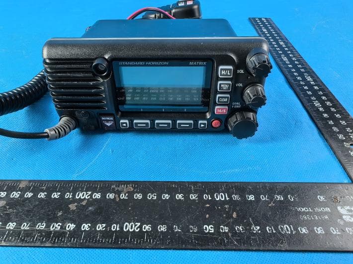
K6630673Y3D
Aug 01, 2024VHF FM Marine Transceiver
Equipment Class
CXX - Communications Rcvr for use w/ licensed Tx and CBs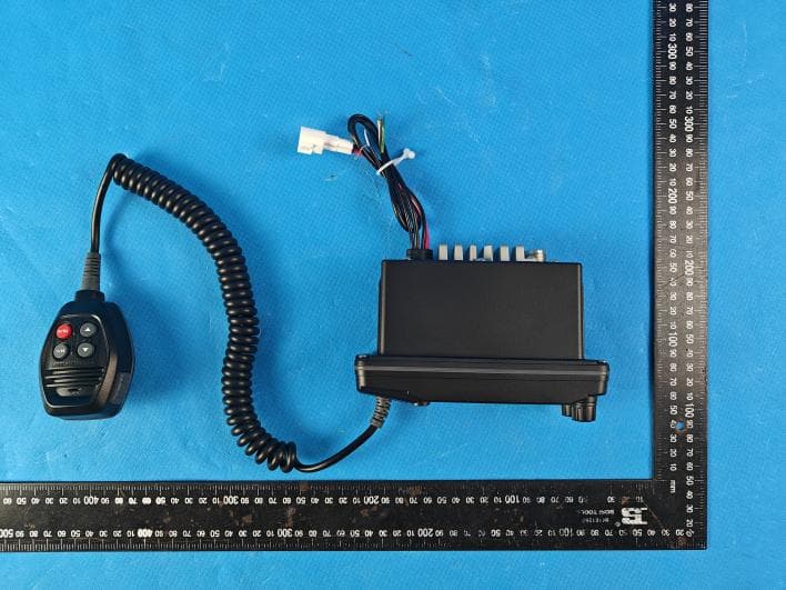
K6630653Y3D
Aug 01, 2024VHF FM Marine Transceiver
Equipment Class
CXX - Communications Rcvr for use w/ licensed Tx and CBs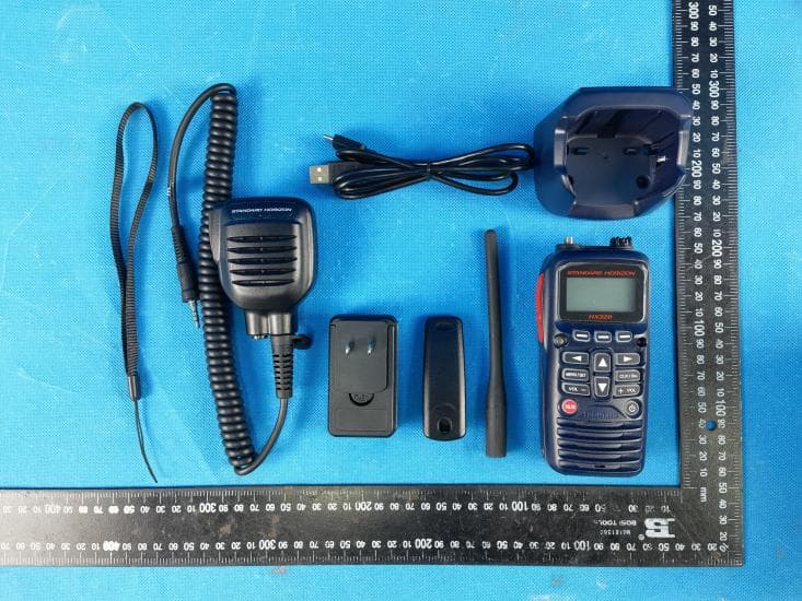
K6630683X30
Jan 10, 2023VHF FM Marine Transceiver
Equipment Class
TNF - Licensed Non-Broadcast Transmitter Held to Face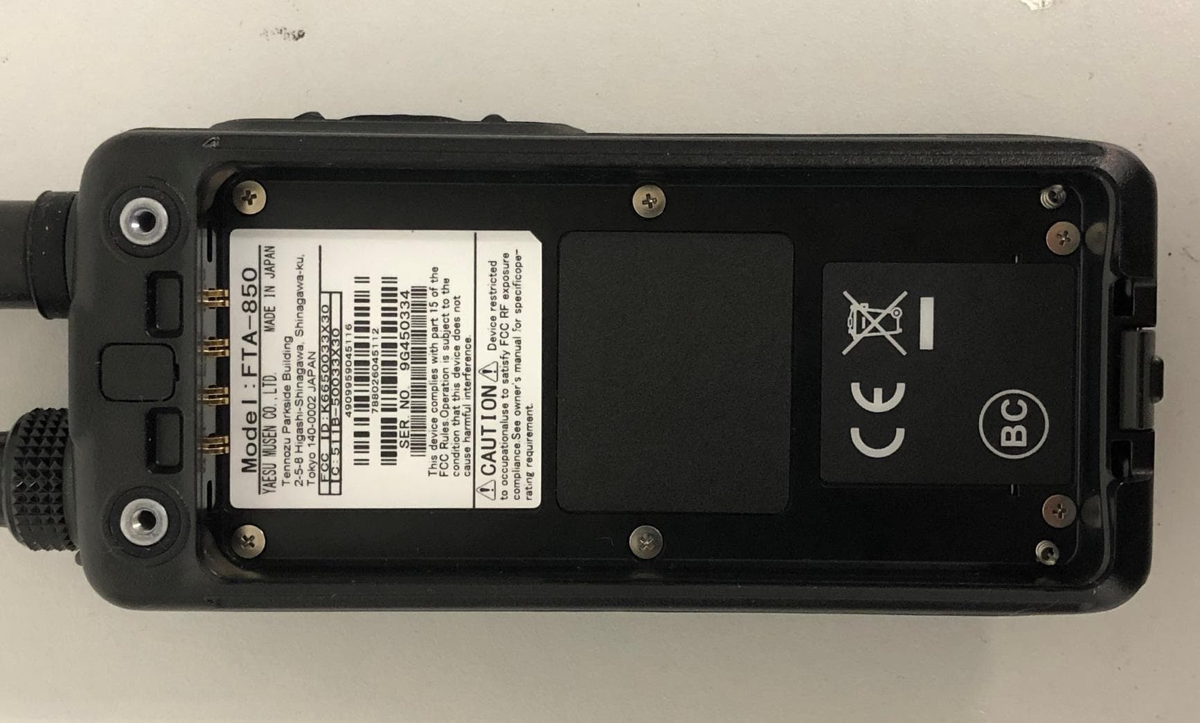
K6650033X30
Nov 18, 2020Airband Radio Transceiver
Equipment Class
TNF - Licensed Non-Broadcast Transmitter Held to Face