K6610723X20PORTABLE RADIO
Yaesu Musen Co., Ltd.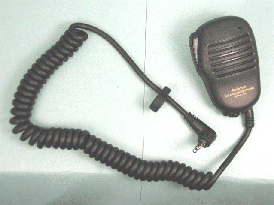
Click to zoom
Application Details
- Equipment Class
- TNF - Licensed Non-Broadcast Transmitter Held to Face
- Date of Grant
- Dec 12, 2006
- Application Purpose
- Original Equipment
- Date of Application
- Dec 07, 2006
- Equipment Note
- PORTABLE RADIO
- Frequency Range
- 118.00000000 - 136.97500000
- Company
- Yaesu Musen Co., Ltd.
- Country
- Japan
Documents & Files
Document Text
Text extracted from the exhibit documents filed with the FCC. Open a document above to read the original.
Users Manual
FCC ID: K6610723X20 IC ID: 511B-10723X20 Operating Manual VXA-220 Operating Manual Introduction The Vertex Standard VXA-220 Pro VI is a compact, stylish, solid hand-held transceiver providing communication (transmit and receive) capability on the International Aircraft Communication Band (“COM” band: 118 ~ 136.975 MHz), and it additionally provides receive on the “NAV” band (108 ~ 117.975 MHz). The VXA-220 boasts 0.7 Watt of clean audio output from its 1.4” (36-mm) diameter loudspeaker, and it also provides 8.33 kHz synthesizer steps for the new narrow-band channel plan. The VXA-220 displays with our exclusive Omni-Glow TM display back-lighting for minimal degradation of your night vision, NOAA weather band monitoring, 8-character Alpha/Numeric Display, 150 Memory Channels, and 100 “Book Memory” Channels. We recommend that you read this manual in its entirety, so as to understand the many features of the VXA-220 completely. Keep this manual handy, so you may use it for reference. Congratulations! You now have at your fingertips a valuable communications tool-a Vertex Standard two-way radio! Rugged, reliable and easy to use, your Vertex Standard radio will keep you in constant touch with your friends and colleagues for years to come, with negligible maintenance down-time. Please take a few minutes to read this manual carefully. The information presented here will allow you to derive maximum performance from your radio, in case questions arise later on. We’re glad you joined the Vertex Standard team. Vertex Standard products cover the entire spectrum of radio communications applications, and our worldwide support network is here to serve you. Let us help you get your message across. Important Notice! FCC RF Exposure Compliance Requirements for Occupational Use Only: This Radio has been tested and complies with the Federal Communications Commission (FCC) RF exposure limits for Occupational Use/Controlled Exposure Environment. In addition, it complies with the following Standards and Guidelines: FCC 96-326, Guidelines for Evaluating the Environmental Effects of Radio-Frequency Radiation. FCC OET Bulletin 65 Edition 97-01 (1997) Supplement C, Evaluating Compliance with FCC Guidelines for Human Exposure to Radio Frequency Electromagnetic Fields. ANSI/IEEE C95.1-1992, IEEE Standard for Safety Levels with Respect to Human Exposure to Radio Frequency Electromagnetic Fields, 3 kHz to 300 GHz. ANSI/IEEE C95.3-1992, IEEE Recommended Practice for the Measurement of Potentially Hazardous Electromagnetic Fields - RF and Microwave. When transmitting, hold the radio in a vertical position with its microphone 1 to 2 inches (2.5 to 5 cm) away from your mouth and keep the antenna at least 1 inch (2.5 cm) away from your head and body. The radio must be used with a maximum operating duty cycle not exceeding 50%, in typical Push-to-Talk configurations. DO NOT transmit for more than 50% of total radio use time (50% duty cycle). Transmitting more than 50% of the time can cause FCC RF exposure compliance requirements to be exceeded. The radio is transmitting when the red LED on the front panel of the radio is illuminated. You can cause the radio to transmit by pressing the P-T-T button. Always use Vertex Standard authorized accessories. 1/21 Vertex Standard Co., Ltd. FCC ID: K6610723X20 IC ID: 511B-10723X20 Operating Manual Controls & Connectors (Top Panel) Antenna Jack This SMA jack accepts the supplied flexible antenna, or another antenna designed to provide 50 Ohm impedance on the Aircraft Communication Band. MIC/EAR Jack You may connect the supplied CT-96 Headset Cable or the (optional) MH-44B4B Speaker/Microphone to this jack. Never connect any Speaker/Microphone that is not recommended by the manufacturer. Because these jack connections are unique, using a Speaker/Microphone that is not specified by Vertex Standard may damage the VXA-220. DIAL Selector Knob This (outer) 20-position detented rotary switch tunes the operating frequency or selects the memory channels. This rotary switch also adjusts the audio volume level by the setting of the Secondary function of the [5(DIAL/▲▼)] key. See page ?? for details. Controls & Connectors (Front Panel) BUSY/TX Indicator Lamp This lamp glows green when a signal is being received, and red when transmitting. Loudspeaker The internal speaker is located in this position. Microphone Speak across this opening in a normal voice level, while pressing the PTT switch, to transmit. LCD (Liquid Crystal Display) The display shows selected operating conditions, as indicated on the next page. Keypad The keypad is used for most radio command operations. Several keys have triple functions. The primary functions are labeled on the key top (activated by simply pressing the key momentarily). The secondary functions are labeled in yellow above the top edge of the key (activated by pressing the [F] key first, then the indicated key). The third functions are labeled in black above the top edge of the key (activated by pressing and holding in the indicated key for 2 seconds). These functions are described in detail on page ??. 2/21 Vertex Standard Co., Ltd. FCC ID: K6610723X20 IC ID: 511B-10723X20 Operating Manual Primary Function (Press Key) Secondary Function (Press [F] + key) Third Function (Press and Hold key for 2 sec.) [1] Frequency Entry Digit 1None None [2)] Frequency Entry Digit 2None None [3] Frequency Entry Digit 3None None [4(TIMER)] Frequency Entry Digit 4Activates the Stop Watch Timer. None [5(DIAL/ )] Frequency Entry Digit 5Exchange the functions of the DIAL and ▲▼keys. None [6(DW)] Frequency Entry Digit 6Activates the Dual Watch feature. Activates the VOX feature. [7(SPL)] Frequency Entry Digit 7Activates Split (Duplex) mode. None [8(Beep)] Frequency Entry Digit 8on/off Switch for Keypad Beeper None [9(SKIP)] Frequency Entry Digit 9Allows Skipping of Channel during Scan. None [0(ANL)] Frequency Entry Digit 0Activates the Automatic Noise Limiter. None [121.5] S…
Text truncated - open the document above for the full version.
Attestation Statements
September 11, 2006 Federal Communications Commission Authorization and Evaluation Division, 7435 Oakland Mills Road Columbia, MD 21046 USA Re: VXA-220 (FCC ID: K6610723X20) Gentlemen: Part 15.19 Compliance Statement is placed on the rear of case. Sincerely, Vertex Standard Co., Ltd. Mr. Moto Kurihara Group Leader of Engineering Division
Attestation Statements
September 11, 2006 Federal Communications Commission Authorization and Evaluation Division, 7435 Oakland Mills Road Columbia, MD 21046 USA Re: VXA-220 (FCC ID: K6610723X20) Gentlemen: A. Part 15.21 Compliance Statement Drawing: Part 15.21: Changes or modifications to this device not expressly approved by Vertex Standard could void the user’s authorization to operate this device. 20mm 97mm B. Part 15.21 Compliance Statement Drawing Location: IN OPERATION MANUAL (location on inside back cover) Sincerely, Vertex Standard Co., Ltd. Mr. Moto Kurihara Group Leader of Engineering Division
Cover Letter(s)
September 11, 2006 Federal Communications Commission EQUIPMENT APPROVAL SERVICES P. O. Box 358315 Pittsburgh, PA 15251-5315 Attention: Authorization and Evaluation Division Reference: VXA-220 (FCC ID: K6610723X20) Pursuant to Sections 0.457 (d)(1)(ii) and 0.459 of the Commission’s Rules, the Applicant hereby requires confidential treatment of some of the information accompanying this Application, as listed below: ・ Block Diagram ・ Schematics These materials contain trade secrets and proprietary information not customarily released to the public. The public disclosure of these matters might be harmful to the Applicant and provide unjustified benefits to its competitors. The Applicant understands that pursuant to Rule 0.457 (d)(1)(ii), disclosure of the Application and all accompanying documentation will not be made before the date of Grant for this Application. Sincerely, Vertex Standard Co., Ltd. Mr. Moto Kurihara Group Leader of Engineering Division
Cover Letter(s)
October 1, 2006 Federal Aviation Administration Office of Spectrum Policy and Management ASR-1 800 Independence Avenue, SW Washington, DC 20591 Re: FAA Notification of FCC Equipment Approval under FCC Part 87 Aviation (Aircraft) Radio FCC ID: K6610723X20 To Whom It May Concern: In accordance with the Federal Communications Commission (FCC) Rules and Regulations, Part 87.147(d), we hereby notify the Federal Aviation Administration (FAA) of its simultaneous filing with the FCC of an application for Certification of the Radio containing the above referenced FCC Identifier. One complete set of the filing documents is enclosed for your review. This will also serve as a request to submit your reply to the following TCB (Telecommunications Certification Body): Timco Engineering, Inc. P.O. Box 370 Newberry, FL 32669 Should you have any questions or require any further information, please do not hesitate to contact me. Sincerely, Vertex Standard Co., Ltd. Moto Kurihara Group Leader of Engineering Division
Cover Letter(s)
KDB Inquiry Tracking Number - 171374
External Photos
FCC ID: K6610723X20 IC ID: 511B-10723X20 Front view with Antenna Front view without Antenna Vertex Standard Co., Ltd. FCC ID: K6610723X20 IC ID: 511B-10723X20 Rear view with Antenna Rear view without Antenna Vertex Standard Co., Ltd. FCC ID: K6610723X20 IC ID: 511B-10723X20 Left view Right view Vertex Standard Co., Ltd. FCC ID: K6610723X20 IC ID: 511B-10723X20 Top view Bottom view Vertex Standard Co., Ltd. FCC ID: K6610723X20 IC ID: 511B-10723X20 Battery Pack Battery Pack Vertex Standard Co., Ltd. FCC ID: K6610723X20 IC ID: 511B-10723X20 Top of Battery Charger Bottom of Battery Charger Vertex Standard Co., Ltd. FCC ID: K6610723X20 IC ID: 511B-10723X20 Top of AC Adapter Bottom of AC Adapter Vertex Standard Co., Ltd. FCC ID: K6610723X20 IC ID: 511B-10723X20 Front of Microphone Back of Microphone Vertex Standard Co., Ltd. FCC ID: K6610723X20 IC ID: 511B-10723X20 Antenna Vertex Standard Co., Ltd.
ID Label/Location Info
VXA-220VXA-220 LABEL DRAWINGLABEL DRAWING Vertex Standard Co., Ltd.Vertex Standard Co., Ltd. ID / Part 15.19 and CAUTION drawings ID drawing Part 15.19 and CAUTION drawings Label location VXA-220 K6610723X20 511B-10723X20 4909959000000 ! ! Device restricted to occupational use to satisfy FCC RF exposure compliance. See owner's manual for specific operating requirement CAUTION This device complies with part 15 of the FCC Rules. Operation is subject to the condition that this device does not cause harmful interference.
ID Label/Location Info
November 23, 2006 Federal Communications Commission Authorization and Evaluation Division 7435 Oakland Mills Road Columbia, MD 21046 Re: VXA-220 (FCC ID: K6610723X20) Gentlemen: Vertex Standard Co., Ltd. requests acceptance of the labeling location proposal described below for transceivers bearing FCC ID: K6610723X20. The subject transceivers are compact, handheld models (as shown in the below photos) and there is no area to fit the label on the surface. Also, the surface area of the panel is of a rough texture and a label would not stay affixed. Because the majority of the transceiver housing is composed of display, speaker, operating controls and a removable battery pack, there is limited space available to attach the required label that contains the FCC ID. The battery pack is removable so putting the label on the back is not an option. For this reason, we propose placing the label, which contains the FCC identifier inside the battery compartment as shown below: Should you have any questions regarding this, please advise. Sincerely, Vertex Standard Co., Ltd. Mr. Moto Kurihara Group Leader of Engineering Division
Internal Photos
FCC ID: K6610723X20 IC ID: 511B-10723X20 Removed Front Panel Side-A of MAIN-UNIT with LCD Vertex Standard Co., Ltd. FCC ID: K6610723X20 IC ID: 511B-10723X20 Side-A of MAIN-UNIT without LCD Side-B of MAIN-UNIT Vertex Standard Co., Ltd. FCC ID: K6610723X20 IC ID: 511B-10723X20 Front of LCD Back of LCD Vertex Standard Co., Ltd. FCC ID: K6610723X20 IC ID: 511B-10723X20 Inside of front panel Inside of chassis Vertex Standard Co., Ltd. FCC ID: K6610723X20 IC ID: 511B-10723X20 Inside of microphone (1) Inside of microphone (2) Vertex Standard Co., Ltd.
Operational Description
FCC ID: K6610723X20 IC ID: 511B-10723X20 Circuit Description VXA-220 Circuit Description Receive Signal Path Incoming RF from the antenna jack is passed through a low-pass filter and high-pass filter consisting of coils L1024, L1027, L1028, L1029, L1030 & L1031, capacitors C1213,C1218,C1219,C1222,C1223,C1224,C1226,C1227,C1228,C1229,C1230, &C1234 and antenna switching diodes D1038 and D1040 to the receiver front end section. Signals within the frequency range of the transceiver is applied to the receiver front end which contains RF amplifier Q1049 and varactor-tuned band-pass filter consisting of coils L1014, L1015, L1018, L1020, L1021, L1025 & L1026, capacitors C1180, C1182, C1184, C1185, C1186, C1190, C1193, C1194, C1197, C1207, C1215 & C1216, and diodes D1035, D1036, D1037 & D1039, then applied to the 1st mixer Q1043. Buffered output from the VCO is amplified by Q1032 to provide a pure 1st local signal between 155.25 and 184.25 MHz for injection to the 1st mixer. The 47.25 MHz 1st mixer product then passes through monolithic crystal filter XF1001 (7.5 kHz BW) which strips away all but the desired signal, which is then amplified by mixer post-amp Q1042. The amplified 1st IF signal is applied to the AM/FM IF subsystem IC Q1039, which contains the 2nd mixer, 2nd local oscillator, limiter amplifier, noise amplifier and AM/FM detector. A 2nd local signal is generated by PLL IC Q1025 from the 11.7 MHz crystal X1002 .The11.7MHz signal is quadruple by Q1037 to produce the 450 kHz 2nd IF when mixed with the 1st IF signal within Q1039. The 2nd IF then passes through the ceramic filter CF1001 to strip away unwanted mixer products. In the FM mode, a 2nd IF signal from the ceramic filter CF1001 applied to the limiter amplifier section of Q1039, which removes amplitude variations in the 450 kHz IF before detection of the speech by the ceramic discriminator CD1001. Detected audio from Q1039 is passed through the de-emphasis, consisting of the resistors R1082, R1083, R1087 & R1090, capacitors C1069, C1070, C1069 & C1081, and Q1019-2. In the AM mode, detected audio from Q1039 is passed through the audio amplifier Q1019-1 and ANL circuit, then applied to the AF amplifier Q1019-2. When impulse noise received, a portion of the AM detector output signal from the AM/FM IF subsystem Q1039, including pulse noise is rectified by D1019. The resulting DC is applied to the ANL MUTE gate Q1022, thus reducing the pulse noises. The processed audio signal from Q1019-1 is passed through the amplifier Q1019-2 to the volume control IC Q1029. The audio signal is passed through the volume control IC to the audio power amplifier Q1003, providing up to 0.7 Watts to 16 Ω loudspeaker. A portion of the AF signal from the AM/FM IF subsystem Q1039 converted into DC voltage within the IC, and provide to the inversion amplifiers Q1048 and Q1050. These amplifier reduce the amplifier gain of the RF amplifier Q1049 while receiving a strong signal. Squelch Control When signal is received, appear the DC squelch control voltage at pin 15 of AM/FM IF subsystem Q1039 according to the receiving signal strength. This DC is applied to pin 16 of microprocessor Q1015. The DC squelch control voltage is compared with the SQL threshold level by the microprocessor Q1015. If the DC squelch control voltage is lower, microprocessor Q1015 control the volume control IC Q1029.and pin14 of Q1029 goes low. thus disabling the AF audio. Also, the microprocessor stops scanning, if active, and allows audio to pass through the the volume control IC Q1029. Transmit Signal Path Speech input from the microphone is passed through the microphone amplifier Q1011-1, 1/3 Vertex Standard Co., Ltd. FCC ID: K6610723X20 IC ID: 511B-10723X20 Circuit Description then applied to the ALC amplifier Q1013. The amplified speech signal is passed through the high-pass filter Q1011-4 and low-pass filter Q1011-3, which adjust the modulation level, then fed to the AM modulator Q1045. When using the optional headset, the SIDETONE signal from J1002 becomes “HIGH”, turning Pin10 of Q1015 on; pin 90 of Q1015 therefore a portion of the speech signal applied to the AF power amplifier Q1001 as a monitor signal. The carrier signal from the VCO Q1028 passes through the buffer amplifier Q1049 and TX/RX switch D1026. The signal from D1026 is amplified by Q1040 and Q1044, and ultimately applied to the final amplifier Q1045 which increases the signal level up to 5 watts output power. The transmit signal then passes through the antenna switch D1038, and is low-pass filtered to suppress away harmonic spurious radiation before delivery to the antenna. Automatic Transmit Power Control RF power output from the final amplifier is sampled by C1217/C1221 and is rectified by D1041. The resulting DC is fed through the Automatic Power Controller Q1047, thus allowing control of the power output. Transmit Inhibit When the transmit PLL is unlocked, pin 7 of PLL chip Q1025 goes to a logic low. The resulting DC “unlock” control voltage is switches off TX inhibit switches Q1035, to disable the supply voltage to transmitter RF amplifiers Q1040, disabling the transmitter. Spurious Suppression Generation of spurious products by the transmitter is minimized by the fundamental carrier frequency being equal to the final transmitting frequency. Additional harmonic suppression is provided by a low-pass filter consisting of L1027, L1029 & L1031 and C1213, C1222, C1224, C1227, C1229 & C1234, resulting in more than 60 dB of harmonic suppression prior to delivery of the RF signal to the antenna. PLL Frequency Synthesizer PLL circuitry consists of VCO Q1028, VCO buffer Q1032 & Q1034, and PLL subsystem IC Q1025, which contains a reference divider, serial-to-parallel data latch, programmable divider, phase comparator and charge pump. Stability is maintained by a regulated 3.5 V supply via Q1033 and 5V supply via Q1031 which feeds the PLL reference oscillator Q1025, as well as capacitors associated with the 11.7 MHz frequency re…
Text truncated - open the document above for the full version.
Parts List/Tune Up Info
FCC ID: K6610723X20 IC ID: 511B-10723X20 Alignment VXA-220 Alignment Introduction The VXA-220 is carefully aligned at the factory for the specified performance across the Aircraft and Weather bands. Realignment should therefore not be necessary except in the event of a component failure. The following procedures cover the adjustments that are not normally required once the transceiver has left the factory. However, if damage occurs and some parts subsequently are replaced, realignment may be required. If a sudden problem occurs during normal operation, it is likely due to component failure; realignment should not be done until after the faulty component has been replaced. We recommend that servicing be performed only by authorized Vertex Standard service technicians who are experienced with the circuitry and fully equipped for repair and alignment. If a fault is suspected, contact the dealer from whom the transceiver was purchased for instructions regarding repair. Under no circumstances should any alignment be attempted unless the normal function and operation of the transceiver are clearly understood, the cause of the malfunction has been clearly pinpointed and any faulty components replaced, and realignment determined to be absolutely necessary. Problems caused by unauthorized attempts at realignment are not covered by the warranty policy Vertex Standard reserves the right to change circuits and alignment procedures, in the interest of improved performance, without notifying owners. The following test equipment (and familiarity with its use) is necessary for complete realignment. While most steps do not require all of the equipment listed, the interactions of some adjustments may require that more complex adjustments be performed afterwards. Do not attempt to perform only a signal step unless it is clearly isolated electrically from all other steps. Have all test equipment ready before beginning, and follow all of the steps in a section in the order presented. Correction of problems caused by misalignment resulting from use of improper test equipment is not covered under the warranty policy. Required Test Equipment ο Radio Tester with calibrated output level at 200 MHz ο In-line Wattmeter with 5 % accuracy at 200 MHz ο 50 Ω, 10 W RF Dummy Load ο Regulated DC Power Supply adjustable from 3 to 15 VDC, 2 A ο Frequency Counter: ±0.2 ppm accuracy at 200 MHz ο AF Signal Generator ο AC Voltmeter ο DC Voltmeter: high impedance ο VHF Sampling Coupler Alignment Preparation & Precautions A 50 Ω RF load and in-line wattmeter must be connected to the main antenna jack in all procedures that call for transmission, except where specified otherwise. Correct alignment is not possible with an antenna. After completing one step, read the next step to see if the same test equipment is required. If not, remove the test equipment (except dummy load and wattmeter, if connected) before proceeding. Correct alignment requires that the ambient temperature be the same as that of the transceiver and test equipment, and that this temperature be held constant between 20 - 30 °C (68 - 86 °F). When the transceiver is brought into the shop from hot or cold air, it should be allowed some time to come to room temperature before alignment. Whenever possible, alignments should be made with oscillator shields and circuit boards firmly affixed 1/4 Vertex Standard Co., Ltd. FCC ID: K6610723X20 IC ID: 511B-10723X20 Alignment in place. Also, the test equipment must be thoroughly warmed up before beginning. Set up the test equipment as shown below for transceiver alignment, apply 7.2 VDC power to the transceiver. Notes: signal levels in dB referred to in alignment are based on 0 dBμ = 0.5 μV (closed circuit). PLL Section PLL Reference Frequency Connect the wattmeter, dummy load and frequency counter connected to the antenna jack, then set the transceiver to 128.000 MHz and turn the transceiver off. Press and hold in the PTT switch, Monitor switch, and ENT key while turn the transceiver on to enter the alignment mode. Rotate the DIAL selector knob to select the “REF xxx.” Press the PTT switch, confirm the counter reading is 128.000 MHz. If not, 1. press the ENT key momentarily, 2. rotate the DIAL selector knob clockwise (frequency up) or counter-clockwise (frequency down), 3. press the ENT key again, 4. confirm the counter reading. Repeat above steps 1 - 4, so that the counter reading is 128.000 MHz (±100 Hz). Turn the transceiver off. Transmitter Section AM TX Power Adjustment Connect the wattmeter and dummy load to the antenna jack, then set the transceiver to 128.000 MHz and turn the transceiver off. Press and hold in the PTT switch, Monitor switch, and ENT key while turn the transceiver on to enter the alignment mode. Rotate the DIAL selector knob to select the “TX PO xxx.” Press the PTT switch with no microphone input, confirm the RF output power is 1.5 Watts. If not, 1. press the ENT key momentarily, 2. rotate the DIAL selector knob clockwise (increase the power) or counter-clockwise (decrease the power), 3. press the ENT key again, 4. confirm the RF output power. Repeat above steps 1 - 4, so that the RF output power is 1.5 Watts. Turn the transceiver off. Tx AM Modulation Adjustment Connect the Radio Tester to the antenna jack, then adjust the AF generator output level for injection of 200 mV rms @ 1 kHz to the MIC jack. Set the transceiver to 127.500 MHz and turn the transceiver off. Press and hold in the PTT switch, Monitor switch, and ENT key while turn the transceiver on to enter the alignment mode. Rotate the DIAL selector knob to select the “ MDLV xxx.” Press the PTT switch, confirm the modulation level is 85 % modulation (±5 %). If not, 1. press the ENT key momentarily, 2. rotate the DIAL selector knob clockwise (increase the MIC gain) or counter-clockwise (decrease the MIC gain), 3. press the ENT key again, 2/4 Vertex Standard Co., Ltd. FCC ID: K6610723X20 IC ID: 511B-10723X…
Text truncated - open the document above for the full version.
Parts List/Tune Up Info
1 FCC ID: K6610723X20/IC ID: 511B-10723X20 VXA-220Semi-Conductor Parts List Address Parts Code Device NameDescriptionTYP VAL MAIN-UNIT D 1001 G2071090 DiodeM1FM3-5063 D 1002 G2071090 DiodeM1FM3-5063 D 1003 G2070634 Diode1SS400 D 1004 G2070998 Zener DiodeEDZ 5.1B D 1005 G2070174 DiodeDAN222 D 1006 G2070178 DiodeDA221 D 1007 G2070850 DiodeRB751S-40 D 1008 G2070584 DiodeHSC277-E D 1009 G2070998 Zener DiodeEDZ 5.1B D 1010 G2070860 LEDCL-165HR/YG-D-T D 1011 G2070634 Diode1SS400 D 1012 G2070178 DiodeDA221 D 1013 G2070596 DiodeHVC350B-E D 1014 G2070584 DiodeHSC277-E D 1015 G2070584 DiodeHSC277-E D 1016 G2070178 DiodeDA221 D 1017 G2070178 DiodeDA221 D 1018 G2070708 DiodeHVC359-E D 1019 G2070634 Diode1SS400 D 1020 G2070634 Diode1SS400 D 1021 G2070634 Diode1SS400 D 1022 G2070634 Diode1SS400 D 1024 G2071116 LEDSML-512DW D 1025 G2071116 LEDSML-512DW D 1026 G2070174 DiodeDAN222 D 1027 G2071116 LEDSML-512DW D 1028 G2070634 Diode1SS400 D 1029 G2071116 LEDSML-512DW D 1030 G2071116 LEDSML-512DW D 1031 G2071116 LEDSML-512DW D 1032 G2071116 LEDSML-512DW D 1033 G2071116 LEDSML-512DW D 1034 G2070634 Diode1SS400 D 1035 G2070596 DiodeHVC350B-E D 1036 G2070596 DiodeHVC350B-E D 1037 G2070596 DiodeHVC350B-E D 1038 G2070128 DiodeRLS135 D 1039 G2070596 DiodeHVC350B-E D 1040 G2070128 DiodeRLS135 D 1041 G2070168 DiodeHSM88WA D 1042 G2070584 DiodeHSC277-E D 1043 G2070584 DiodeHSC277-E D 1044 Q9000847 Surge Absorber TVSF0603 D 1045 G2070584 DiodeHSC277-E D 1046 G2070634 Diode1SS400 DS1001 G6090178 LCDAC072N Q 1001 G3070075 TransistorDTC144EE Q 1002 G3070223 TransistorCPH6102 Q 1003 G1091542 ICTDA2822D013 Q 1004 G3070075 TransistorDTC144EE Q 1005 G3117748R Transistor2SA1774 R Q 1006 G3346178R Transistor2SC4617 R Q 1007 G3070223 TransistorCPH6102 Vertex Standard Co.,Ltd. 2 FCC ID: K6610723X20/IC ID: 511B-10723X20 VXA-220Semi-Conductor Parts List Address Parts Code Device NameDescriptionTYP VAL Q 1008 G1092838 ICAK93C95AF E-1 Q 1009 G3070195 Transistor2SB1201S Q 1010 G3070075 TransistorDTC144EE Q 1011 G1094009 ICLM2902PWR Q 1012 G3346178R Transistor2SC4617 R Q 1013 G1093114 ICAN6123MS Q 1014 G3070088 TransistorUMG2N Q 1015 G1094209 ICLC87F7BC8A-F56G2-E Q 1016 G3070343 TransistorUMD5N Q 1017 G3346178R Transistor2SC4617 R Q 1018 G3070252 TransistorDTA143EE Q 1019 G1094009 ICLM2902PWR Q 1020 G3346178R Transistor2SC4617 R Q 1021 G3070264 TransistorDTA114TE Q 1022 G3070088 TransistorUMG2N Q 1023 G3070075 TransistorDTC144EE Q 1024 G3346178R Transistor2SC4617 R Q 1025 G1092545 ICMB15A01PFV1-G-BND-EFE1 Q 1026 G3070343 TransistorUMD5N Q 1027 G1093606 ICS-80835CNMC-B8U-G Q 1028 G3352318H Transistor2SC5231C8 Q 1029 G1093033 ICM62364FP 600D Q 1030 G3070078 TransistorUMW1N Q 1031 G3070223 TransistorCPH6102 Q 1032 G3355557 Transistor2SC5555ZD Q 1033 G1093672 ICS-812C35AUA-C2P Q 1034 G3355557 Transistor2SC5555ZD Q 1035 G3070343 TransistorUMD5N Q 1037 G3349158O Transistor2SC4915-O Q 1038 G3070265 TransistorCPH6202 Q 1039 G1093013 ICTK10931V-G Q 1040 G3352268E Transistor2SC5226-5 Q 1041 G3070265 TransistorCPH6202 Q 1042 G3349158O Transistor2SC4915-O Q 1043 G4803188 MOSFET3SK318 Q 1044 G3070321 MOSFETRD01MUS1 Q 1045 G3070352 MOSFETRD07MVS1A Q 1046 G3070343 TransistorUMD5N Q 1047 G1093969 ICLMV321IDCKR Q 1048 G3346178R Transistor2SC4617 R Q 1049 G4803188 MOSFET3SK318 Q 1050 G3346178R Transistor2SC4617 R Q 1051 G3070076 TransistorUMD2N Vertex Standard Co.,Ltd.
Test Report
Page 1 of 29 REPORT ON Radio testing of the VERTEX STANDARD VXA-220 In accordance with ANSI/TIA/EIA-603, RSS141 September 2006Report number TA000388 Vertex Standard Co., Ltd. GENERAL INFORMATION TRANSMITTERS Switchable Variable xN/A RECEIVERS This re port was prepared by Vertex Standard Co., Ltd. 2000 300 DC ANSI/TIA/EIA-603 6K00A3E [MHz] [W] 137to108 Date 08 / September /2006 Test performed by M.Kurihara INPUT IMPEDANCE (RF): INTERMEDIATE FREQUENCIES: FREQUENCY RANGE: OUTPUT IMPEDANCE (RF): Collector Voltage: Collector Current: MODEL NAME: INPUT IMPEDANCE (MIC): MAXIMUM POWER RATING: [V] VXA-220 K6610723X20 VERTEX STANDARD (Carrier) [W] AUDIO OUTPUT POWER: OUTPUT IMPEDANCE (SP): [Ω] 8 0.7 50 [Ω] [MHz] [kHz] 47.25 450 1st 2nd [MHz] [W] [Ω] [Ω] POWER OUTPUT RATING: 118137to to1.5 FREQUENCY RANGE: 0.8[A] MANUFACTURER: Report number TA000388Page 2 of 29 7.4[V] Vertex Standard Co., Ltd. RSS141 50 TRADE NAME: VHF AM Transceiver 6K000001 TYPE OF EMISSION: 7.4VOLTAGE RQUIREMENTS: SERIAL NUMBER: SPECIFICATION ARE REFERENC E EUT DESCRIPTION: FCC ID: IC ID:511B-10723X20 Vertex Standard Co., Ltd. Report number TA000388Page 3 of 29 VXA-220 Channel Settin gs Hi ghLow 1118.0500118.050118.05025k1.5W- 2128.0500128.050128.05025k1.5W- 3136.9750136.975136.97525k1.5W- 4108.0500-108.05025k-- 5 6 7 8 9 10 11 12 13 14 15 16 Power Transmit Frequency [MHz] CH No. Receive Frequency [MHz] CH SpacingShown on LCD Vertex Standard Co., Ltd. NAME OF TEST:R.F. Power Output (Conducted) SPECIFICATION:47 CFR 2.1046 (a) GUIDE:ANSI/TIA/EIA-603, Paragraph 2.2.1 TEST EQUIPMENT: As per attached page The EUT was connected to a resistive coaxial attenuator of normal load impedance, and the modulated output powerwas measured by means of an R.F. power meter. Measurement accuracy is ± 4 % NAME OF TEST:R.F. Power Output (Radiated) High Power MEASUREMENT PROCEDURE 118.0500 HIGHLOW 2 3 FREQUENC Y TUNED, MHz 11.490 128.050 136.975 1.470 1.340 1. 2. MEASUREMENT RESULTS 118.050 CHANNEL R.F. POWER, WATTS NOMINAL, MHz dBm LEVEL, 26.5 Report number TA000388Page 4 of 29 136.975022.9 128.050021.1 Vertex Standard Co., Ltd. (2)(3)(4) Serial Numbe rDescription Page 5 of 29 (5) TRANSMITTER POWER CONDUCTED MEASUREMENTS TEST 1: R.F. POWER OUTPUT TEST 2: FREQUENCY STABILIT Y Power Supply Instruments Test Sample (1) Report number TA000388 (2) RF COUPLER ADVANTEST TR4153 WEINSCHELL 49-10-43*** *** *** Agilent 8901B POWER MODE*** Agilent 8482B (5) FREQUENCY COUNTER gilent 8901B FREQUENCY MOD*** (1) COAXUAL ATTENUATOR (4) POWER METER (3) POWER SENSOR Vertex Standard Co., Ltd. NAME OF TEST:Unwanted Emissions …
Text truncated - open the document above for the full version.
Contact Information
Applicant
Masatoshi Muraishi(Engineering Division)
Test Firm
Timco Engineering, Inc.Sid Sanders
Technical Specifications
| # | Rule Parts | Frequency Range | Power Output | Emission | Tolerance |
|---|---|---|---|---|---|
| 1 | 87 | 118 MHz - 136.975 MHz | 1.5 W | 6K00A3E | 10.0000000000 ppm |
Other Applications from Yaesu Musen Co., Ltd.
K660E180X10
Dec 01, 2025BLUETOOTH MICROPHONE
Equipment Class
DTS - Digital Transmission System
K6630673Y3D
Aug 01, 2024VHF FM Marine Transceiver
Equipment Class
CXX - Communications Rcvr for use w/ licensed Tx and CBs
K6630653Y3D
Aug 01, 2024VHF FM Marine Transceiver
Equipment Class
CXX - Communications Rcvr for use w/ licensed Tx and CBs
K6630683X30
Jan 10, 2023VHF FM Marine Transceiver
Equipment Class
TNF - Licensed Non-Broadcast Transmitter Held to Face
K6650033X30
Nov 18, 2020Airband Radio Transceiver
Equipment Class
TNF - Licensed Non-Broadcast Transmitter Held to Face