K6630073X20HX270S MARINE HT RADIO
Yaesu Musen Co., Ltd.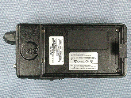
Click to zoom
Application Details
- Equipment Class
- GVH - Part 80 VHF Transmitter (GMDSS)
- Date of Grant
- Jul 01, 2004
- Application Purpose
- Original Equipment
- Date of Application
- Jul 01, 2004
- Equipment Note
- HX270S MARINE HT RADIO
- Frequency Range
- 156.02500000 - 157.42500000
- Company
- Yaesu Musen Co., Ltd.
- Country
- Japan
Documents & Files
Document Text
Text extracted from the exhibit documents filed with the FCC. Open a document above to read the original.
Users Manual
FCC ID: K6630073X20 IC ID: 511B-30073X20 Operating Manual 1/14 Vertex Standard Co., Ltd. HX270S Operating Manual SAFETY TRANING INFORMATION This Radio has been tested and complies with the Federal Communications Commission (FCC) RF exposure limits for Occupational Use/Controlled exposure environment. In addition, it complies with the following Standards and Guidelines: - FCC 96-326, Guidelines for Evaluating the Environmental Effects of Radio-Frequency Radiation. - FCC OET Bulletin 65 Edition 97-01 (1997) Supplement C, Evaluating Compliance with FCC Guidelines for Human Exposure to Radio Frequency Electromagnetic Fields. - ANSI/IEEE C95.1-1992, IEEE Standard for Safety Levels with Respect to Human Exposure to Radio Frequency Electromagnetic Fields, 3kHz to 300 GHz. - ANSI/IEEE C95.3-1992, IEEE Recommended Practice for the Measurement of Potentially Hazardous Electromagnetic Fields-RF and Microwave. WARNING: This radio generates RF electromagnetic energy during transmit mode. This radio is designed for and classified as Occupational Use Only, meaning it must be used only during the course of employment by individuals aware of the hazards, and the ways to minimize such hazards. This radio is not intended for use by the General Population in an uncontrolled environment. CAUTION: To ensure that your expose to RF electromagnetic energy is within the FCC allowable limits for occupational use, always adhere to the following guidelines: - This radio is NOT approved for use by the general population in an uncontrolled environment. This radio is restricted to occupational use, work related operations only where the radio operator must have the knowledge to control its RF exposure conditions. - When transmitting, hold the radio in a vertical position with its microphone 1 to 2 inches (2.5 to 5 cm) away from your mouth and keep the antenna at least 1 inch (2.5cm) away from your head and body. - The radio must be used with a maximum operating duty cycle not exceeding 50 %, in typical Push-to-Talk (PTT) configurations. DO NOT transmit for more than 50 % of total radio use time (50 % duty cycle). Transmitting more than 50 % of the time can cause FCC RF exposure compliance requirements to be exceeded. The radio is transmitting when the red LED on the top of the radio is illuminated. You can cause the radio to transmit by pressing the PTT button. - DO NOT transmit when the radio is used in Body Worn configuration with the following accessory: belt-clip (CLIP-14). It must be used ONLY for (1) there is a 4 cm distance from the body during transmitting, (2) monitoring purposes, using the speaker only and (3) for carrying purposes. - Always use Standard Horizon authorized accessories. The information listed above provides the user with the information needed to make him or her aware of RF exposure, and what to do to assure that this radio operates with the FCC RF exposure limits of this radio. Electromagnetic Interference/Compatibility During transmissions, this radio generates RF energy that can possibly cause interference with other devices or systems. To avoid such interference, turn off the radio in areas where signs are posted to do so. Do not operate the transmitter in areas that are sensitive to electromagnetic radiation such as hospitals, health care facilities, aircraft, and blasting sites. FCC ID: K6630073X20 IC ID: 511B-30073X20 Operating Manual 2/14 Vertex Standard Co., Ltd. FCC LICENSE INFORMATION This radio operates on communications frequencies which are subject to FCC (Federal Communications Commission) Rules and Regulations. FCC Rules require that all operators using Marine / Private Land Mobile radio frequencies obtain a radio license before operating their equipment. FCC ID: K6630073X20 IC ID: 511B-30073X20 Operating Manual 3/14 Vertex Standard Co., Ltd. 1. GENERAL INFORMATION 1.1 INTRODUCTION The HX270S is a handheld two-way VHF transceiver. The transceiver has marine, 10 weather (WX) channels. The marine and land channels are selectable to comply with either USA, International, or Canadian regulations. It has an emergency channel 16 which can be immediately selected from any channel by pressing the 16/9 key. Weather channels can also be accessed immediately by pressing the WX key. The transceiver includes following features: memory scanning, Priority Scanning, weather alert, battery saver, easy-to-read large LCD display, EEPROM memory back-up, battery life displayed on LCD, and a transmit time-out timer (TOT). 1.2 FCC/INDUSTRY CANADA INFORMATON The following data pertaining to the transceiver is necessary to fill out the license application. FCC Type Accepted: Part 80 Output Power with FNB-83: 1 watt (Low), 2.5 watts (Mid), and 5 watts (High) Emission: 16K0G3E (Voice) / 16K0G2B (ATIS) Frequency Range: 156.025-157.425 MHz FCC Type Number: Industry Canada Type Approval: Additional FCC and Industry Canada data, including licensing requirements, are contained in the companion document titled OWNWER’S MANUAL SUPPLEMENT. The document also contains charts for VHF channel assignments, transceiver operating procedures, maintenance, factory service information, and warranty data. 2. ACCESSORIES 2.1 PACKING LIST When the package containing the transceiver is first opened, please check it for the following contents: • HX270STransceiver • FNB-83Ni-MH Battery Pack • CD-26Charger Cradle • NC-88B120VAC Wall Charger for CD-26 • CAT-460Antenna • CLIP-14Belt Clip with screw • Lanyard • Owner’s Manual • Owner’s Manual Supplement 2.2 OPTIONS FBA-25AAlkaline Battery Case E-DC-19DC Cable with 12 V Cigarette Lighter Plug for CD-26 E-DC-6DC Cable; plug and wire only for CD-26 MCC460 Soft Case FCC ID: K6630073X20 IC ID: 511B-30073X20 Operating Manual 4/14 Vertex Standard Co., Ltd. 3. CONTROLS AND INDICATORS NOTE: This section defines each control of the transceiver. For detailed operating instructions refer to section 4 of this manual. Refer to Figure 1 for the location of the following controls, indicators, and …
Text truncated - open the document above for the full version.
External Photos
FCC ID: K6630073X20 IC ID: 511B-30073X20 Vertex Standard Co., Ltd. Front view with Antenna Rear view with Antenna FCC ID: K6630073X20 IC ID: 511B-30073X20 Vertex Standard Co., Ltd. Front view without Antenna Rear view without Antenna FCC ID: K6630073X20 IC ID: 511B-30073X20 Vertex Standard Co., Ltd. Rear view without Battery Pack Left view FCC ID: K6630073X20 IC ID: 511B-30073X20 Vertex Standard Co., Ltd. Right view Top view FCC ID: K6630073X20 IC ID: 511B-30073X20 Vertex Standard Co., Ltd. Bottom view Antenna FCC ID: K6630073X20 IC ID: 511B-30073X20 Vertex Standard Co., Ltd. Battery Pack Battery Pack FCC ID: K6630073X20 IC ID: 511B-30073X20 Vertex Standard Co., Ltd. Top of Battery Charger (CD-26) Bottom of Battery Charger FCC ID: K6630073X20 IC ID: 511B-30073X20 Vertex Standard Co., Ltd. Top of AC Adapter (NC-83B) Bottom of AC Adapter
Internal Photos
FCC ID: K6630073X20 IC ID: 511B-30073X20 Vertex Standard Co., Ltd. Removed Front Panel Side-A of MAIN-UNIT FCC ID: K6630073X20 IC ID: 511B-30073X20 Vertex Standard Co., Ltd. Side-B of MAIN-UNIT Inside of front panel FCC ID: K6630073X20 IC ID: 511B-30073X20 Vertex Standard Co., Ltd. Inside of chassis
Operational Description
FCC ID: K6630073X20 IC ID: 511B-30073X20 Circuit Description 1/3 Vertex Standard Co., Ltd. HX270S Circuit Description 1. Receive Signal Path Incoming RF from the antenna jack is delivered to the RF Unit and passes through a low- pass filter consisting of coils L1025, L1026, and L1027, capacitors C1229, C1235, C1237, C1241, C1243, C1245 and C1246, and antenna switching diode D1033. Signals within the frequency range of the transceiver enter a Varactor-tuned band-pass filter consisting of coils L1019 and L1022, capacitors C1217, C1218 and C1250, and diodes D1030, then amplified by Q1044 and enter a Varactor-tuned band-pass filter consisting of coils L1016, L1017 and L1018, capacitors C1182, C1184, C1185, C1186, C1187, C1188, C1191, C1192, C1195, C1197, and C1199, and diodes D1026, D1027, and D1028, before first mixing by Q1041. Buffered output from the VCO is amplified by Q1023 to provide a pure first local signal between 134.35 and 141.575 MHz for injection to the first mixer Q1041. The 21.7 MHz first mixer product then passes through monolithic crystal filter XF1001/XF1002 to strip away all but the desired signal, which is then amplified by Q1037. The amplified first IF signal is applied to FM IF subsystem IC Q1033, which contains the second mixer, second local oscillator, limited amplifier, noise amplifier, and RSSI amplifier. A second local signal is produced from the PLL reference/second local oscillator of X1001 (21.25 MHz). The 21.25 MHz reference signal is delivered to mixer section of Q1033 which produce the 450 kHz second IF mixed with the first IF signal. The second IF then passes through the ceramic filter CF1001 to strip away unwanted mixer products, and is then applied to the limited amplifier in Q1033, which removes amplitude variations in the 450kHz IF, before detection of the speech by the ceramic discriminator CD1001. 2.Audio Amplifier The demodulated audio signal from the Q1033 passes through a band-pass filter and High-pass filter, then applied to the de-emphasis. Then passes through the audio volume and the audio power amplifier Q1009, providing up to 400 mW of audio power to the 4 Ω loudspeaker. 3. Squelch Control The squelch circuitry consists of a noise amplifier and band-pass filter and noise detector within Q1033. When no carrier received, noise at the output of the detector stage in Q1033 is amplified and band-pass filtered by the noise amplifier section of Q1033 and the network between pins 7 and 8, and then rectified by detection circuit in Q1033. The resulting DC squelch control voltage is passed to pin 73 of the microprocessor Q1043. If no carrier is received, this signal causes pin 67 of Q1043 to go low and pin 66 to go high. Pin 66 signals of Q1043 to disable the supply voltage to the audio amplifier Q1009, while pin 18 hold the green (Busy) half of the LED off. Thus, the microprocessor blocks output from the audio amplifier, and silences the receiver, while no signal is being received (and during transmission, as well). When a carrier appears at the discriminator, noise is removed from the output, causing pin 75 of Q1039 to go low and the microprocessor to activate the ”Busy” LED via Q1053. The microprocessor then checks for CTCSS or CDCSS code squelch information, if enabled. If not transmitting and CTCSS or CDCSS is not activated, or if the received tone or code matches that programmed, allows audio to pass through the audio amplifier Q1009 to the loudspeaker by enabling the supply voltage to it via Q1014. 4. Transmit Signal Path The speech input from the microphone MC1001 passes through the audio amplifier FCC ID: K6630073X20 IC ID: 511B-30073X20 Circuit Description 2/3 Vertex Standard Co., Ltd. Q1051, which is adjusted the microphone gain. The speech signal passes through pre- emphasis circuit to Q1051, which contains the IDC, and low-pass filter. The filtered audio signal is applied to Q1030 which is adjusted the audio level, then is applied to varactor diode D1007, which frequency modulates the VCO Q1012. A portion of the audio signal from Q1030 is applied to X1001. The processed audio may then be mixed with a CTCSS tone generated by Q1043 for frequency modulation of the PLL carrier (up to ±5 kHz from the unmodulated carrier) at the transmitting frequency. If a CDCSS code is enabled for transmission, the code is generated by microprocessor Q1043 and delivered to X1001 (21.25 MHz) for CDCSS modulating. The modulated signal from the VCO Q1012 is buffered by Q1013. The low-level transmit signal is then passes through the TX switching diode D1010 to the buffer amplifier Q1031, driver amplifier Q1034, then amplified transmit signal is applied to the final amplifier Q1036 up to 5.0 watts output power. The transmit signal then passes through the antenna switch D1031 and is low-pass filtered to suppress harmonic spurious radiation before delivery to the antenna. 4-1 Automatic Transmit Power Control Current from the final amplifier is sampled by C1238, C1239, C1242 and C1244, and R1261, and R1267, and is rectified by Q1032. The resulting DC is fed back through Q1032 to the drive amplifier Q1034 and final amplifier Q1036, for control of the power output. The microprocessor selects ”High” or “Low” power levels. 4-2 Spurious Suppression Generation of spurious products by the transmitter is minimized by the fundamental carrier frequency being equal to final transmitting frequency, modulated directly in the transmit VCO. Additional harmonic suppression is provided by a low-pass filter consisting of coils L1012 and L1013 plus capacitors C1148, C1153, C1154, C1159, C1163 and C1172, resulting in more than 60 dB of harmonic suppression prior to delivery to the antenna. 5. PLL Frequency Synthesizer The PLL circuitry on the Main Unit consists of VCO Q1012, VCO buffer Q1013, PLL subsystem IC Q1015, which contains a reference divider, serial-to-parallel data latch, programmable divider, phase comparator and charge pump, and crystal X1001 which frequency stability is ±5 pp…
Text truncated - open the document above for the full version.
Parts List/Tune Up Info
1/2 FCC ID: K6630073X20 IC ID: 511B-30073X20 Component Applications Address Device nameDescriptionApplication [MAIN-UNIT] D 1001 Diode1SS400Riple Filter D 1002 Zener DiodeEDZ TE61 5.1BProtect D 1003 Diode1SS400Mic Mute D 1004 Varactor DiodeHVC350BVCO Modulator D 1005 DiodeRB521S-30CPU Back up D 1006 DiodeHSC277VCO Shift SW D 1007 DiodeHSC277VCO Modulator D 1008 Varactor DiodeHVC350BREF Tune D 1009 DiodeDA221CPU Reset D 1010 DiodeDAN235ETX/RX RF SW D 1011 Diode1SS400Level Shift D 1012 DiodeDA221SQL Noise Detect D 1013 DiodeDA221SQL Noise Detect D 1014 LED19-215UYOC/S530A2LED Indicator D 1015 LED19-215UYOC/S530A2LED Indicator D 1016 LED19-215UYOC/S530A2LED Indicator D 1017 LED19-215UYOC/S530A2LED Indicator D 1018 LED19-215UYOC/S530A2LED Indicator D 1019 LED19-215UYOC/S530A2LED Indicator D 1020 LEDCL-165HR/YGLED Indicator D 1021 Diode1SS400Level Shift D 1022 Diode1SS400Level Shift D 1023 DiodeDA221Limiting Diode D 1024 Diode1SS400Protect D 1025 DiodeDA221Limiting Diode D 1026 Varactor DiodeHVC350BBPF Tune D 1027 Varactor DiodeHVC350BBPF Tune D 1028 Varactor DiodeHVC350BBPF Tune D 1029 Diode1SS400Limiting Diode D 1030 Varactor Diode1SV323BPF Tune D 1031 DiodeRLS135ANT SW D 1032 Diode1SS321Power Detect D 1033 DiodeRLS135ANT SW D 1034 Serge absorberTVSF0805**Serge absorber D 1035 Serge absorberTVSF0805**Serge absorber Q 1001 Transistor2SC4617Riple Filter Q 1002 TransistorDTA114TESave SW Q 1003 ICLM2904PWRAPC AMP Q 1004 TransistorDTA114TESave SW Q 1005 TransistorDTC143ZEVOL Control SW Q 1006 Transistor2SC4617Save SW Q 1007 TransistorDTA144EEPTT Control Q 1008 TransistorDTC144EE TLPLL Loop Filter SW Q 1009 ICTDA2822D013AF Power AMP Q 1010 ICS-812C30AMC-C2K3V Regulator Q 1011 Transistor2SA1774PLL Lock Detect Q 1012 Transistor2SC5231VCO Q 1013 Transistor2SC5374VCO Buff AMP Q 1014 TransistorFMMTL718AF Power AMP Control Q 1015 ICMB15A01PFVPLL Subsystem Q 1016 Transistor2SC4617AF Power AMP Control Q 1017 TransistorFMMTL7185V Regulator Q 1018 TransistorUMW1N5V Regulator Q 1019 Transistor2SA1774AF Power AMP Control Q 1020 Transistor2SC5374Buff AMP Q 1021 ICBD4845FVECPU Reset Q 1023 Transistor2SC5374Buff AMP Q 1024 Transistor2SA1774TX/RX SW Q 1025 TransistorUMW1NTX/RX SW Q 1026 Transistor2SC4617CPU Reset Q 1027 TransistorDTA143XETX/RX SW Q 1028 TransistorFMMTL618LED Indicator Control Q 1029 Transistor2SC4617LED Indicator Control Q 1030 ICM62364FPD/A Convertor Q 1031 Transistor2SC5226TX Buff AMP Q 1032 Transistor2SC4617LED Indicator Control Q 1033 ICNJM2591VIF Subsystem Q 1034 FET2SK3074TX Driver AMP HX270S Vertex Standard Co., Ltd. 2/2 FCC ID: K6630073X20 IC ID: 511B-30073X20 Component Applications Address Device nameDescriptionApplication HX270S Q 1035 FET2SJ364RX AF Mute Q 1036 FETRD07MVS1RF Power AMP Q 1037 Transistor2SC44001st IF AMP Q 1038 Transistor2SC4617AF BPF AMP Q 1039 TransistorUMD2NClone Control Q 1040 Transistor2SC4617AF BPF AMP Q 1041 FET3SK3201st Mixer Q 1042 ICBR24L64F-WE2Programmable Data Store Q 1043 ICHD64F38024WMicroproccesor Q 1044 Transistor2SC5006RX RF AMP Q 1045 Transistor2SC5374Clock Shift Q 1050 ICLM2904PWRDC Buff AMP Q 1051 ICLM2902PWRMic AMP Q 1052 ICLM2904PWRWX Filter Vertex Standard Co., Ltd.
RF Exposure Info
FCC RF Exposure Requirements General information: FCCID: K6630073X20 Device category: Portable per Part 2.1093 Environment: Occupational/Controlled Exposure Operating configuration and exposure conditions: This device does not have any connector for use of an external speaker/microphone or headset accessories. The belt-clip specified with this device is only use for carrying purposes. This radio cannot be operated while body-worn. According to July 17, 2002 TCB exclusion list, the low threshold is calculated as follows: For d > or = 2.5cm, 900/0.156 = 5.8Watt for 50% Operating Duty Cycle. For 100% Duty cycle the threshold is 11.6Watt. The maximum measured output power for this device is 5Watt at 100% Duty Cycle. Conclusion: SAR testing is not required to qualify for TCB approval. 7/2/2004 Page 1 of 1 FCCID: K6630073X20
Test Report
TIMCO ENGINEERING INC. 849 NW State Road 45 Newberry, Florida 32669 http://www.timcoengr.com 888.472.2424 F 352.472.2030 email: [email protected] APPLICANT: VERTEX STANDARD CO., LTD. Test Report Product Name: HX270S MARINE HT RADIO FCC ID: K6630073X20 Applicant: VERTEX STANDARD CO., LTD. 4-8-8 NAKAMEGURO, MEGURO-KU TOKYO 153-8644 JAPAN Date Receipt: MAY 24, 2004 Date Tested: JUNE 15, 2004 FCC ID: K6630073X20 REPORT #: V\VERTEX\732AUT4\732AUT4TestReport.doc COVER SHEET TIMCO ENGINEERING INC. 849 NW State Road 45 Newberry, Florida 32669 http://www.timcoengr.com 888.472.2424 F 352.472.2030 email: [email protected] APPLICANT: VERTEX STANDARD CO., LTD. TABLE OF CONTENTS LIST APPLICANT: VERTEX STANDARD CO., LTD. FCC ID: K6630073X20 TEST REPORT: PAGE 1............GENERAL INFORMATION & TECHNICAL DESCRIPTION PAGE 2............TECHNICAL DESCRIPTION CONTINUED RF POWER OUTPUT PAGE 3............TECHNICAL DATA PAGE 4............VOICE MODULATION CHARACTERISITICS AUDIO FREQUENCY RESPONSE PAGE 5............AUDIO LOW PASS FILTER PAGE 6............MODULATION LIMITING PAGE 7............OCCUPIED BANDWIDTH PAGE 8............OCCUPIED BANDWIDTH PLOT PAGE 9............SPURIOUS EMISSIONS AT ANTENNA TERMINALS PAGE 10...........METHOD OF MEASURING CONDUCTED SPURIOUS EMISS PAGE 11-12........FIELD STRENGTH OF SPURIOUS EMISSIONS PAGE 13...........METHOD OF MEASURING RADIATED SPURIOUS EMISSIONS PAGE 14...........FREQUENCY STABILITY PAGE 15...........LIST OF TEST EQUIPMENT EXHIBITS INCLUDING: REQUEST FOR CONFIDENTIALITY LETTER BLOCK DIAGRAM SCHEMATIC PARTS LIST USERS MANUAL LABEL SAMPLE & LOCATION EXTERNAL PHOTOGRAPHS INTERNAL PHOTOGRAPHS ALIGNMENT PROCEDURE OPERATIONAL DESCRIPTION TEST SET UP PHOTOGRAPHS FCC ID: K6630073X20 REPORT #: V\VERTEX\732AUT4\732AUT4TestReport.doc TABLE OF CONTENTS TIMCO ENGINEERING INC. 849 NW State Road 45 Newberry, Florida 32669 http://www.timcoengr.com 888.472.2424 F 352.472.2030 email: [email protected] APPLICANT: VERTEX STANDARD CO., LTD. GENERAL_INFORMATION 2.1033(c) VERTEX STANDARD CO., LTD. will sell the FCC ID: K6630073X20 VHF Marine transmitter in quantity, for use under FCC RULES PART 80. 2.1033(c) TECHNICAL_DESCRIPTION (4) Type of Emission: 16K0G3E/16K0F3E Bn = 2M + 2DK M = 3000 D = 4.6KHz (Peak Deviation) K = 1 Bn = 2(3.0K) + 2(4.6K)(1) = 6.0K + 9.2 = 15.2K 80.205 (a) ALLOWED AUTHORIZED BANDWIDTH = 20.00KHz. 2.1033(c)(6) Frequency Range: 156.025 – 157.425 MHz 2.1033(c)(7) Power Range and Controls: There is a user Power switch for High/Low Power. Maximum Output Power Rating: High PWR Watts, PWR1 Watt into a 50 ohm resistive load. 2.1033(c)(8) DC Voltages and Current into Final Amplifier: POWER INPUT FINAL AMPLIFIER ONLY High Low Vce = 7.2 Volts Vce = 7.2 Volts Ice = 1.53 A. Ice = 0.61 A. Pin = 11.02 Watts Pin = 4.29 Watts Function of each electron tube or semiconductor device or other active circuit device is included in the parts list exhibit. FCC ID: K6630073X20 REPORT #: V\VERTEX\732AUT4\732AUT4TestReport.doc Page 1 of 15 TIMCO ENGINEERING INC. 849 NW State Road 45 Newberry, Florida 32669 http://www.timcoengr.com 888.472.2424 F 352.472.2030 email: [email protected] APPLICANT: VERTEX STANDARD CO., LTD. 2.1033(c)(9) Complete Circuit Diagrams: The circuit diagrams and block diagrams are included. 2.1033(c)(10) Instruction book. The instruction manual is included. 2.1033(c)(11) Tune-up procedure. The tune-up procedure is included. Description of all circuitry and devices provided for determining and stabilizing frequency is included in the circuit description 2.1033(c)(11) Digital modulation. This unit does NOT use digital modulation. The data required by 2.1046 through 2.1055 is submitted below. 2.1046(a) RF_power_output. 80.215 (e)(1) RF power is measured by connecting a 50 ohm, re- sistive wattmeter to the RF output connector. With a nominal battery voltage of 7.2 V, and the transmitter properly adjusted the RF output measures: OUTPUT POWER: HIGH: 5.0 W CONDUCTED LOW: 1.0 W CONDUCTED METHOD OF MEASURING RF POWER OUTPUT Transmitter 50 ohm under test Resistive Wattmeter Power Supply FCC ID: K6630073X20 REPORT #: V\VERTEX\732AUT4\732AUT4TestReport.doc Page 2 of 15 TIMCO ENGINEERING INC. 849 NW State Road 45 Newberry, Florida 32669 http://www.timcoengr.com 888.472.2424 F 352.472.2030 email: [email protected] APPLICANT: VERTEX STANDARD CO., LTD. TECHNICAL DATA: 80.203 (b) External Controls: The transmitter is capable of changing frequency between 156.025 – 157.425 MHz by external control. The available channels are shown in the User Manual description Channel List. These channels are preprogrammed by the manufacturer and change of frequency is inaccessible to the station operator. 80.203 (c) Five minutes continuous transmission test. The antenna was connected to a dummy load and the radio was locked in a transmit PTT mode. An external timer digital clock was used to observe the duration of the un-modulated transmission. The transmitter turned off and the radio went to receive mode at 4 minutes, 58 seconds as displayed by the external digital clock. FCC ID: K6630073X20 REPORT #: V\VERTEX\732AUT4\732AUT4TestReport.doc Page 3 of 15 TIMCO ENGINEERING INC. 849 NW State Road 45 Newberry, Florida 32669 http://www.timcoengr.com 888.472.2424 F 352.472.2030 email: [email protected] APPLICANT: VERTEX STANDARD CO., LTD. 2.1047(a) Voice Modulation_characteristics: (b) AUDIO_FREQUENCY_RESPONSE See the following plot. 732aut4 audio frequency response -30 +10 -20 -10 +0 d B 100 20k 200 500 1k 2k 5k 10k 2.85988k 2.85988k Hz FCC ID: K6630073X20 REPORT #: V\VERTEX\732AUT4\732AUT4TestReport.doc Page 4 of 15 TIMCO ENGINEERING INC. 849 NW State Road 45 Newberry, Florida 32669 http://www.timcoengr.com 888.472.2424 F 352.472.2030 email: [email protected] APPLICANT: VERTEX STANDARD CO., LTD. 2.1047(a) 80.213(e) AUDIO_LOW_PASS_FILTER The audio low pass filter shown in the following plot. FCC ID: K6630073X20 REPORT #: V\VERTEX\732AUT4\732AUT4TestReport.doc Page 5 of 15 TIMCO ENGINEERING INC. 849 NW State Road 4…
Text truncated - open the document above for the full version.
Contact Information
Applicant
Masatoshi Muraishi(Engineering Division)
Test Firm
Timco Engineering, Inc.S Sanders
Technical Specifications
| # | Rule Parts | Frequency Range | Power Output | Emission | Tolerance |
|---|---|---|---|---|---|
| 4 | 80.1101(c)(4) | 156.025 MHz - 157.425 MHz | 1 W | 16K0G3E | 10 ppm |
Other Applications from Yaesu Musen Co., Ltd.
K660E180X10
Dec 01, 2025BLUETOOTH MICROPHONE
Equipment Class
DTS - Digital Transmission System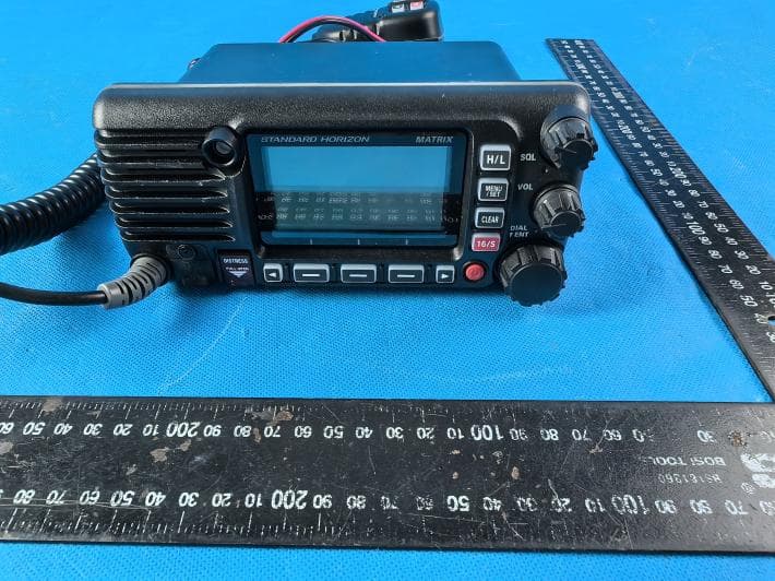
K6630673Y3D
Aug 01, 2024VHF FM Marine Transceiver
Equipment Class
CXX - Communications Rcvr for use w/ licensed Tx and CBs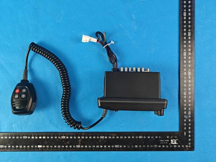
K6630653Y3D
Aug 01, 2024VHF FM Marine Transceiver
Equipment Class
CXX - Communications Rcvr for use w/ licensed Tx and CBs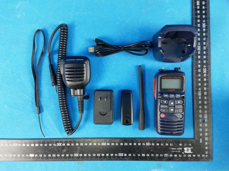
K6630683X30
Jan 10, 2023VHF FM Marine Transceiver
Equipment Class
TNF - Licensed Non-Broadcast Transmitter Held to Face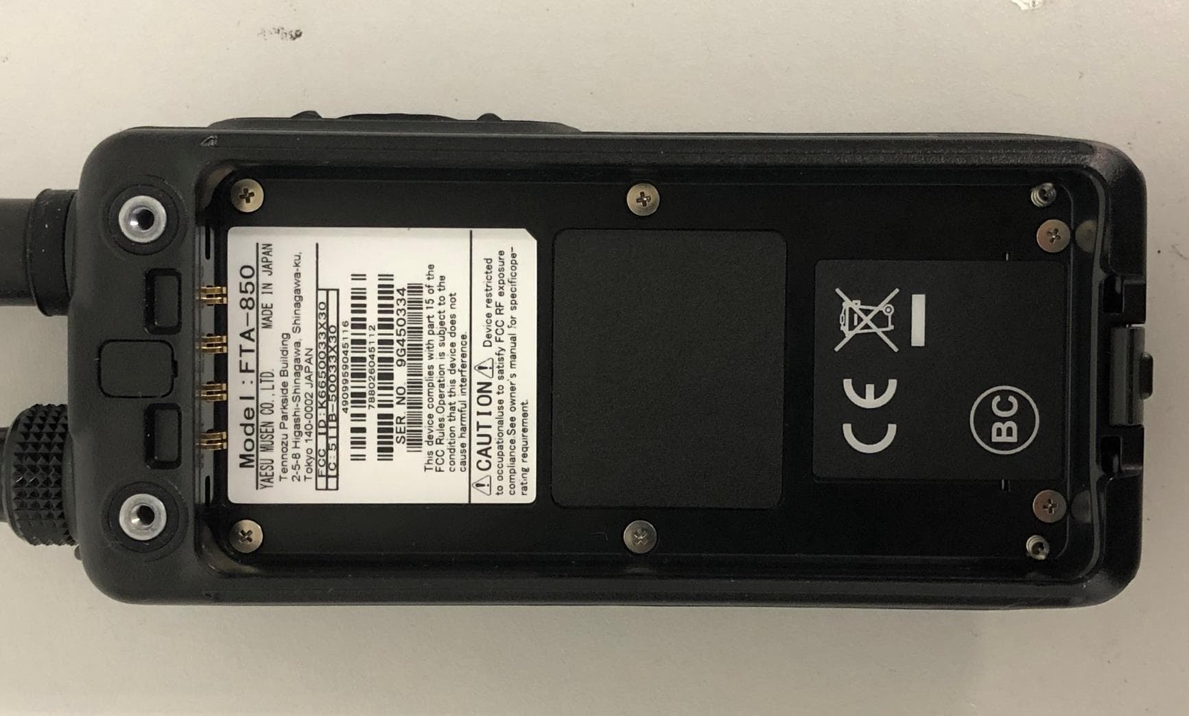
K6650033X30
Nov 18, 2020Airband Radio Transceiver
Equipment Class
TNF - Licensed Non-Broadcast Transmitter Held to Face