K6630183X20PORTABLE MARINE VHF TRANSCEIVER
Yaesu Musen Co., Ltd.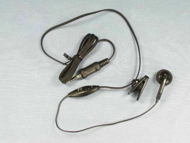
Click to zoom
Application Details
- Equipment Class
- TNF - Licensed Non-Broadcast Transmitter Held to Face
- Date of Grant
- Jan 22, 2006
- Application Purpose
- Original Equipment
- Date of Application
- Jan 22, 2006
- Equipment Note
- PORTABLE MARINE VHF TRANSCEIVER
- Frequency Range
- 156.02500000 - 157.42500000
- Company
- Yaesu Musen Co., Ltd.
- Country
- Japan
Documents & Files
Document Text
Text extracted from the exhibit documents filed with the FCC. Open a document above to read the original.
Users Manual
FCC ID: K6630183X20 IC ID: 511B-30183X20 Operating Manual 1/41 Vertex Standard Co., Ltd. HX500S Operating Manual FCC ID: K6630183X20 IC ID: 511B-30183X20 Operating Manual 2/41 Vertex Standard Co., Ltd. Table of Contents FCC ID: K6630183X20 IC ID: 511B-30183X20 Operating Manual 3/41 Vertex Standard Co., Ltd. Congratulations on your purchase of the HX500S! Whether this is your first portable marine VHF transceiver, or if you have other STANDARD HORIZON equipment, the STANDARD HORIZON organization is committed to ensuring your enjoyment of this high performance transceiver, which should provide you with many years of satisfying communications even in the harshest of environments. STANDARD HORIZON technical support personnel stands behind every product sold, and we invite you to contact us should you require technical advice or assistance. We appreciate your purchase of the HX500S, and encourage you to read this manual thoroughly, so as to learn and fully understand the capabilities of the HX500S. WARNING This radio is capable of transmitting on VHF Marine. The FCC allows the use of VHF Marine band on water areas only. However the FCC does not allow the use of the VHF Marine band when on land. If persons use the VHF Marine Band on land and interfere with others communicating, the FCC will be notified and search for the interference. Responsible parties found to be transmitting on the VHF Marine Band on land could be fined up to $10,000 for the first offense. The FCC does however prohibit the use in aircraft. FCC ID: K6630183X20 IC ID: 511B-30183X20 Operating Manual 4/41 Vertex Standard Co., Ltd. SAFETY TRANING INFORMATION This Radio has been tested and complies with the Federal Communications Commission (FCC) RF exposure limits for Occupational Use/Controlled exposure environment. In addition, it complies with the following Standards and Guidelines: - FCC 96-326, Guidelines for Evaluating the Environmental Effects of Radio-Frequency Radiation. - FCC OET Bulletin 65 Edition 97-01 (1997) Supplement C, Evaluating Compliance with FCC Guidelines for Human Exposure to Radio Frequency Electromagnetic Fields. - ANSI/IEEE C95.1-1992, IEEE Standard for Safety Levels with Respect to Human Exposure to Radio Frequency Electromagnetic Fields, 3kHz to 300 GHz. - ANSI/IEEE C95.3-1992, IEEE Recommended Practice for the Measurement of Potentially Hazardous Electromagnetic Fields-RF and Microwave. WARNING: This radio generates RF electromagnetic energy during transmit mode. This radio is designed for and classified as Occupational Use Only, meaning it must be used only during the course of employment by individuals aware of the hazards, and the ways to minimize such hazards. This radio is not intended for use by the General Population in an uncontrolled environment. CAUTION: To ensure that your expose to RF electromagnetic energy is within the FCC allowable limits for occupational use, always adhere to the following guidelines: - This radio is NOT approved for use by the general population in an uncontrolled environment. This radio is restricted to occupational use, work related operations only where the radio operator must have the knowledge to control its RF exposure conditions. - When transmitting, hold the radio in a vertical position with its microphone 1 to 2 inches (2.5 to 5 cm) away from your mouth and keep the antenna at least 1 inch (2.5cm) away from your head and body. - The radio must be used with a maximum operating duty cycle not exceeding 50 %, in typical Push-to-Talk (PTT) configurations. DO NOT transmit for more than 50 % of total radio use time (50 % duty cycle). Transmitting more than 50 % of the time can cause FCC RF exposure compliance requirements to be exceeded. The radio is transmitting when the red LED on the top of the radio is illuminated. You can cause the radio to transmit by pressing the PTT button. - DO NOT transmit when the radio is used in Body Worn configuration with the following FCC ID: K6630183X20 IC ID: 511B-30183X20 Operating Manual 5/41 Vertex Standard Co., Ltd. accessory: belt-clip. It must be used ONLY for (1) there is a 4 cm distance from the body during transmitting, (2) monitoring purposes, using the speaker only and (3) for carrying purposes. - Always use STANDARD HORIZON authorized accessories. The information listed above provides the user with the information needed to make him or her aware of RF exposure, and what to do to assure that this radio operates with the FCC RF exposure limits of this radio. Electromagnetic Interference/Compatibility During transmissions, this radio generates RF energy that can possibly cause interference with other devices or systems. To avoid such interference, turn off the radio in areas where signs are posted to do so. Do not operate the transmitter in areas that are sensitive to electromagnetic radiation such as hospitals, health care facilities, aircraft, and blasting sites. FCC ID: K6630183X20 IC ID: 511B-30183X20 Operating Manual 6/41 Vertex Standard Co., Ltd. FCC AND CANADA RADIO LICENSE INFORMATION Standard Horizon radios comply with the Federal Communication Commission (FCC) and Industry-Canada requirements that regulate the Maritime Radio Service. MARITIME STATION LICENSE An FCC ship station license is no longer required for any vessel traveling in U.S. waters which uses a VHF marine radio, RADAR or EPIRB, and which is not required to carry radio equipment. However, any vessel required to carry a marine radio on an international voyage, carrying a HF single side band radiotelephone or marine satellite terminal. FCC license forms, including applications for ship (506) and land station licenses can be downloaded via the Internet at www.fcc.gov/forms. To obtain a form from the FCC, call (888) 225-5322. MARINE RADIO CALL SIGN Currently the FCC does not require recreational boaters to have a Ship Radio Station License. The USCG recommends the boats registration number and the state to be used. CANADIAN SHIP STATION LICENSING You…
Text truncated - open the document above for the full version.
Attestation Statements
November 17, 2005 Federal Communications Commission Authorization and Evaluation Division, 7435 Oakland Mills Road Columbia, MD 21046 USA Re: HX500S (FCC ID: K6630183X20) Gentlemen: Part 15.19 Compliance Statement is placed on the rear of case. Sincerely, Vertex Standard Co., Ltd. Mr. Moto Kurihara Group Leader of Engineering Division
Attestation Statements
November 17, 2005 Federal Communications Commission Authorization and Evaluation Division, 7435 Oakland Mills Road Columbia, MD 21046 USA Re: HX500S (FCC ID: K6630183X20) Gentlemen: A. Part 15.21 Compliance Statement Drawing: B. Part 15.21 Compliance Statement Drawing Location: IN OPERATION MANUAL (location on the back cover page) Sincerely, Vertex Standard Co., Ltd. Mr. Moto Kurihara Group Leader of Engineering Division Part 15.21: Changes or modifications to this device not expressly approved by Vertex Standard could void the user’s authorization to operate this device. 20mm 97mm
Cover Letter(s)
November 17, 2005 Federal Communications Commission EQUIPMENT APPROVAL SERVICES P. O. Box 358315 Pittsburgh, PA 15251-5315 Attention: Authorization and Evaluation Division Reference: HX500S (FCC ID: K6630183X20) Pursuant to Sections 0.457 (d)(1)(ii) and 0.459 of the Commission’s Rules, the Applicant hereby requires confidential treatment of some of the information accompanying this Application, as listed below: ・ Block Diagram ・ Schematics These materials contain trade secrets and proprietary information not customarily released to the public. The public disclosure of these matters might be harmful to the Applicant and provide unjustified benefits to its competitors. The Applicant understands that pursuant to Rule 0.457 (d)(1)(ii), disclosure of the Application and all accompanying documentation will not be made before the date of Grant for this Application. Sincerely, Vertex Standard Co., Ltd. Mr. Moto Kurihara Group Leader of Engineering Division
External Photos
FCC ID: K6630183X20 IC ID: 511B-30183X20 Vertex Standard Co., Ltd. Front view with Antenna Rear view with Antenna FCC ID: K6630183X20 IC ID: 511B-30183X20 Vertex Standard Co., Ltd. Front view without Antenna Rear view without Antenna FCC ID: K6630183X20 IC ID: 511B-30183X20 Vertex Standard Co., Ltd. Left view Right view FCC ID: K6630183X20 IC ID: 511B-30183X20 Vertex Standard Co., Ltd. Top view Bottom view FCC ID: K6630183X20 IC ID: 511B-30183X20 Vertex Standard Co., Ltd. Battery Pack Battery Pack FCC ID: K6630183X20 IC ID: 511B-30183X20 Vertex Standard Co., Ltd. Top of Battery Charger (CD-30) Bottom of Battery Charger FCC ID: K6630183X20 IC ID: 511B-30183X20 Vertex Standard Co., Ltd. Top of AC Adapter (PA-38B) Bottom of AC Adapter FCC ID: K6630183X20 IC ID: 511B-30183X20 Vertex Standard Co., Ltd. Antenna Speaker/Microphone (CMP460) FCC ID: K6630183X20 IC ID: 511B-30183X20 Vertex Standard Co., Ltd. Speaker/Microphone (MH-57A4B) VOX Headset (VC-24) FCC ID: K6630183X20 IC ID: 511B-30183X20 Vertex Standard Co., Ltd. Earpiece Microphone (VC-27)
ID Label/Location Info
HX500SHX500S LABEL DRAWINGLABEL DRAWING Vertex Standard Co., Ltd.Vertex Standard Co., Ltd. ID / Part 15.19 and CAUTION drawings ID drawing Part 15.19 and CAUTION drawings Label location HX500S K6630183X20 511B-30183X20 4909959000000 ! ! Device restricted to occupational use to satisfy FCC RF exposure compliance. See owner's manual for specific operating requirement CAUTION This device complies with part 15 of the FCC Rules. Operation is subject to the condition that this device does not cause harmful interference.
Internal Photos
FCC ID: K6630183X20 IC ID: 511B-30183X20 Vertex Standard Co., Ltd. Removed Front Panel Side-A of MAIN-UNIT with LCD FCC ID: K6630183X20 IC ID: 511B-30183X20 Vertex Standard Co., Ltd. Side-A of MAIN-UNIT without LCD Side-B of MAIN-UNIT FCC ID: K6630183X20 IC ID: 511B-30183X20 Vertex Standard Co., Ltd. LCD LCD FCC ID: K6630183X20 IC ID: 511B-30183X20 Vertex Standard Co., Ltd. Inside of front panel Inside of chassis
Operational Description
FCC ID: K6630183X20 IC ID: 511B-30183X20 Circuit Description 1/3 Vertex Standard Co., Ltd. HX500S Circuit Description Receiver Signal Flow VHF Bands Reception Received VHF bands signals pass through the low-pass filter/high-pass filter circuit, T/R switch circuit composed of diode switch D1048 (RLS135), D1049 (1SV307), and protector diode D1050 (1SS302) before additional filtering by a high-pass filter prior to application to RF amplifier Q1065 (2SC5555). The amplified RF signal is passed through the band-pass filter to first mixer Q1042 (3SK318). Meanwhile, VHF output from the VCO is applied through diode Band switch D1025 (1SS400) and T/R switch D1026 (DAN222) to mixer Q1042 as the first local signal. The TUNE-voltage from the D/A converter Q1014 (M62364PF) is amplified by DC amplifier Q1037 (2SA1774-R) and Q1039 (UMW1), and applied to varactors D1033, D1035, D1038, and D1039 (HVC369B), D1028, D1029, D1036, D1037, D1040, and D1041 (1SV325) in the variable frequency band-pass filters. By changing the electrostatic capacitance of the varactors, optimum filter characteristics are provided for each specific operating frequency. First Intermediate Frequency The 47.25 MHz first intermediate frequency from first mixers is passed through 47.25 MHz monolithic crystal filter (MCF) XF1001 to IF amplifier Q1072 (2SC4915-0) for input to pin 16 of Narrow IF IC Q1063 (TA31136FN) after amplitude limiting by D1045 (DA221). Meanwhile, a portion of the output of 11.7 MHz crystal X1001 is multiplied fourfold by Q1070 (2SC4617-R) and Q1077 (2SC4915-0) to provide the 46.8 MHz second local signal, applied to the IF IC. Within the IC, this signal is mixed with the 47.25 MHz first intermediate frequency signal to produce the 450 kHz second intermediate frequency. This second IF is filtered by ceramic filter CF1001 (LTWC450F) and amplified by the limiting amplifier within the IF IC before quadrate detection by ceramic discriminator CD1001 (JTBC450C7). Demodulated audio is output from pin 9 of the IF IC. The demodulated audio signal from the Q1063 passes through a band-pass filter and squelch gate Q1029 (NJM12902V) before de-emphasis filter. The resulting audio is amplified by AF amplifier Q1009 (TDA7233D) and output through MIC/EAR jack J1001 to internal speaker or an external earphone. Squelch Control Signal components in the neighborhood of 15 kHz contained in the discriminator output pass through an active band-pass filter composed of R1226, R1230, R1239, C1176, C1182 and the operational amplifier between pins 7 and 8 within IF IC Q1063. They are then rectified by D1032 and D1034 (DA221) to obtain a DC voltage corresponding to the level of noise. This FCC ID: K6630183X20 IC ID: 511B-30183X20 Circuit Description 2/3 Vertex Standard Co., Ltd. voltage is input to pin 16 of CPU Q1026 (LC87F5BP8A-F56G2), which compares the input voltage with a previously set threshold. When the input voltage drops below the threshold, normally due to the presence of a carrier, turning on squelch gate Q1029 and allowing any demodulated audio to pass. At the same time, Q1002 and/or Q1004 and/or Q1006 goes on, causing the BUSY/TX lamp D1009 (SDDF01000A) to light. Transmitter Signal Flow Transmit/Receive Switching Closing PTT switch S1002 pulls the base of Q1008 (DTA144EE) low, causing the collector to go high. This signal is input to pin 22 (PTT) of CPU Q1026, allowing the CPU to recognize that the PTT switch has been pushed. When the CPU detects closure of the PTT switch, pin 31 (TX/RX) goes high. This control signal is switches Q1083 (UMD5N). At the same time, PLL division data is input to PLL IC Q1027 (MB15A01PFV1) from the CPU, to disable the receiver power saver. Also, switching Q1076 (UMB3N) to disable the receiver circuits. Then causing the red side of BUSY/TX lamp D1009 to light. Modulation Voice signal input from either built-in microphone MC1001 (SKB-2244S) or external jack J1001 is pre-emphasized by C1020 and R1034, and processed by microphone amplifier Q1010 (NJM12902AV), IDC (instantaneous deviation control) circuit to prevent over-modulation, and active low-pass filter. Transmission Modulating audio passes through deviation setting D/A converter Q1014 to MOD of the VCO. This signal is applied to varactor D1016 (HSC277) in the tank circuit of VCO Q1034 (2SC5555), which oscillates at the desired transmitting frequency. The modulated VCO signal is buffered by amplifier Q1040 (2SC5555) and delivered through T/R diode switch D1026. The modulated low-level transmit signal from the VCO is applied to amplifier Q1048 (2SC5226-5). The modulated transmit signal from the VCO is amplified by Q1056 (2SK3475) and RF power amplifier Q1066 (2SK3476) up to 5 W. The RF output passes through TX diode switch D1048. RF output is passed by T/R switch and low-pass filter to suppress harmonics and spurious products before output to the antenna at the antenna terminal. PLL Frequency Synthesizer PLL IC Q1027 consists of a data shift register, reference frequency divider, phase comparator, charge pump, intermittent operation circuit, and band selector switch. Serial PLL data from the CPU is converted into parallel data by the shift register in the PLL IC and is latched into the comparative frequency divider and reference frequency divider to set a frequency dividing ratio for each. An 11.7 MHz reference signal produced by X1001 is input to REF pin 1 of the PLL IC. The internal reference frequency divider divides the 11.7 MHz reference by 2,340 (or 1,872) to obtain a reference frequency of 5 kHz (or 6.25 kHz), which is applied to the phase comparator. Meanwhile, a sample of the FCC ID: K6630183X20 IC ID: 511B-30183X20 Circuit Description 3/3 Vertex Standard Co., Ltd. output of VCO Q1040 is input to the PLL IC, where it is frequency-divided by the internal comparative frequency divider to produce a comparative frequency also applied to the phase comparator. The phase comparator compares the phase between the reference frequency and comparative freq…
Text truncated - open the document above for the full version.
Parts List/Tune Up Info
FCC ID: K6630183X20 IC ID: 511B-30183X20 Alignment 1/3 Vertex Standard Co., Ltd. HX500S Alignment The HX500S has been carefully aligned at the factory for the specified performance across the land mobile band. Realignment should therefore not be necessary except in the event of a component failure. All component replacement and service should be performed only by an authorized STANDARD HORIZON representative, or the warranty policy may be voided. The following procedures cover the sometimes critical and tedious adjustments that are not normally required once the transceiver has left the factory. However, if damage occurs and some parts are replaced, realignment may be required. If a sudden problem occurs during normal operation, it is likely due to component failure; realignment should not be done until after the faulty component has been replaced. We recommend that servicing be performed only by authorized STANDARD HORIZON service technicians who are experienced with the circuitry and fully equipped for repair and alignment. Therefore, if a fault is suspected, contact the dealer from whom the transceiver was purchased for instructions regarding repair. Authorized STANDARD HORIZON service technicians realign all circuits and make complete performance checks to ensure compliance with factory specifications after replacing any faulty components. Those who do undertake any of the following alignments are cautioned to proceed at their own risk. Problems caused by unauthorized attempts at realignment are not covered by the warranty policy. Also, STANDARD HORIZON must reserve the right to change circuits and alignment procedures in the interest of improved performance, without notifying owners. Under no circumstances should any alignment be attempted unless the normal function and operation of the transceiver are clearly understood, the cause of the malfunction has been clearly pinpointed and any faulty components replaced, and the need for realignment determined to be absolutely necessary. The following test equipment (and thorough familiarity with its correct use) is necessary for complete realignment. Correction of problems caused by misalignment resulting from use of improper test equipment is not covered under the warranty policy. While most steps do not require all of the equipment listed, the interactions of some adjustments may require that more complex adjustments be performed afterwards. Do not attempt to perform only a single step unless it is clearly isolated electrically from all other steps. Have all test equipment ready before beginning, and follow all of the steps in a section in the order presented. Required Test Equipment ο Radio Tester with calibrated output level at 200 MHz ο In-line Wattmeter with 5% accuracy at 200 MHz ο 50 Ω, 10 W RF Dummy Load ο Regulated DC Power Supply adjustable from 3 to 15 VDC, 2A ο Frequency Counter: ±0.2 ppm accuracy at 200 MHz ο AF Signal Generator ο AC Voltmeter ο DC Voltmeter: high impedance ο VHF Sampling Coupler Alignment Preparation & Precautions A 50 Ω RF load and in-line wattmeter must be connected to the main antenna jack in all procedures that call for transmission, except where specified otherwise. Correct alignment is not possible with an antenna. After completing one step, read the next step to see if the same test equipment is required. If not, remove the test equipment (except dummy load and wattmeter, if connected) before proceeding. Correct alignment requires that the ambient temperature be the same as that of the transceiver and test equipment, and that this temperature be held constant between 20 ~ FCC ID: K6630183X20 IC ID: 511B-30183X20 Alignment 2/3 Vertex Standard Co., Ltd. 30 °C (68 ~ 86 °F). When the transceiver is brought into the shop from hot or cold air, it should be allowed some time to come to room temperature before alignment. Whenever possible, alignments should be made with oscillator shields and circuit boards firmly affixed in place. Also, the test equipment must be thoroughly warmed up before beginning. Set up the test equipment as shown below for transceiver alignment, apply 7.2 VDC power to the transceiver. Notes: signal levels in dB referred to in alignment are based on 0 dBμ = 0.5 μV (closed circuit). PLL Section PLL Reference Frequency Connect the wattmeter, dummy load, and frequency counter to the antenna jack. Set the transceiver to CH16 (156.800 MHz) then turn the transceiver off. Press and hold in the PTT key, MONI key, [▲] and [▼] key while turn the transceiver on to enter the alignment mode. Press the [▼] or [▲] key to select the display to [REF xx]. Press the [MEM] key to enable adjustment of the PLL Reference Frequency. Press the PTT key to transmit the transceiver, if necessary, press the [ ▼ ] or [ ▲ ] key to adjust the frequency so the counter frequency is 156.800 MHz (±100 Hz). Press the [MEM] key to exit this Alignment Mode. Press and hold the [PWR] key for 2 seconds to exit to the normal operation. Receiver Section Squelch Hysteresis Adjustment Connect the Radio Tester to the antenna jack. Set the transceiver to CH16 (156.800 MHz) then turn the transceiver off. Press and hold in the PTT key, MONI key, [▲] and [▼] key while turn the transceiver on to enter the alignment mode. Press the [ ▼ ] or [ ▲ ] key to select the display to [FM HS xx]. Press the [MEM] key to enable adjustment of this Alignment Mode. Press the [ ▼ ] or [ ▲ ] key to adjust the hysteresis level. Press the [MEM] key to exit this Alignment Mode. Squelch Threshold Adjustment Adjust the Radio Tester output level -13 dBμ (with a standard FM modulation: ±3.0 kHz deviation @ 1 kHz) at 156.800 MHz. Press the [ ▼ ] or [ ▲ ] key to select the display to [FM TH xx]. Press the [MEM] key to read the Squelch Threshold data. Press the [MEM] key again to save the new setting. Squelch Tight Adjustment Adjust the Radio Tester output level +5 dBμ (with a standard FM modulation: ±3.0 kHz deviation @ 1 kH…
Text truncated - open the document above for the full version.
Parts List/Tune Up Info
Page 1/3 HX500S Address Device name DescriptionTYP VALUE [MAIN-UNIT] Q 1001 Transistor 2SC4617 Q 1002 Transistor FMMTL618TA Q 1003 Not used Q 1004 Transistor FMMTL618TA Q 1005 Transistor CPH6202 Q 1006 Transistor FMMTL618TA Q 1007 Not used Q 1008 Transistor DTA144EE Q 1009 ICTDA2822D Q 1010 ICNJM12902V Q 1011 Transistor UMD5N Q 1012 Transistor FMMTL718TA Q 1014 ICM62364FP Q 1015 Not used Q 1016 Transistor 2SA1774 Q 1017 Transistor 2SC4617 Q 1020 ICBR24L64F Q 1022 Not used Q 1023 Not used Q 1024 Transistor DTC143ZE Q 1025 Not used Q 1026 ICLC87F7BC8A-F56G2 Q 1027 ICMB15A01PFV1 Q 1028 Not used Q 1029 ICNJM12902V Q 1031 Not used Q 1032 Not used Q 1033 ICBU4094BCFV Q 1034 Transistor 2SC5555ZD Q 1036 Transistor 2SC4617 Q 1037 Transistor 2SA1774 Q 1039 Transistor UMW1N Q 1040 Transistor 2SC5555ZD Q 1041 Transistor DTC144EE Q 1042 Transistor 3SK318 Q 1043 Transistor UMA4N Q 1044 Not used Q 1045 ICNJM12904R Q 1046 Transistor 2SC4617 Q 1047 Not used Q 1048 Transistor 2SC5226-5 Q 1049 Not used Q 1051 Not used Q 1052 ICS-80835CNMC-B8U Q 1053 Not used Q 1054 ICNJM2125F Q 1055 Not used Q 1056 Transistor 2SK3475 Q 1057 Not used Q 1058 ICS-812C35AUA-C2P Q 1059 Transistor UMW1N Q 1060 Transistor CPH6102 Q 1061 Not used Q 1062 Not used Q 1063 ICTA31136FN Q 1064 Not used Q 1065 Transistor 2SC5555ZD Q 1066 Transistor 2SK3476 Q 1067 Not used Q 1068 Not used Q 1069 Not used Q 1070 Not used FCC ID: K6630183X20 IC ID: 511B-30183X20 Semi-Conductor Parts List Vertex Standard Co., Ltd. Page 2/3 HX500S Address Device name DescriptionTYP VALUE FCC ID: K6630183X20 IC ID: 511B-30183X20 Semi-Conductor Parts List Q 1071 Not used Q 1072 Transistor 2SC4915 Q 1073 Not used Q 1074 Not used Q 1075 Transistor 2SC4617 Q 1076 Transistor UMB3N Q 1077 Transistor 2SC4915 Q 1078 Not used Q 1079 Not used Q 1080 Not used Q 1081 Not used Q 1082 Not used Q 1083 Transistor UMD5N D 1001 LED19-215UYOC/S530A2 D 1002 LED19-215UYOC/S530A2 D 1003 LEDBRPG1211C-TR D 1004 LED19-215UYOC/S530A2 D 1005 Zener Diode UDZS TE-17 5.1B D 1006 Not used D 1007 LED19-215UYOC/S530A2 D 1008 LED19-215UYOC/S530A2 D 1009 Not used D 1010 LED19-215UYOC/S530A2 D 1011 LEDCL-191WA-D-T D 1012 LED19-215UYOC/S530A2 D 1013 DiodeDA221 D 1014 Diode1SS400 D 1015 Varactor Diode 1SV325 D 1016 DiodeHSC277 D 1017 DiodeHVC359 D 1018 Not used D 1019 Not used D 1020 Not used D 1021 DiodeDAN222 D 1022 DiodeDAN222 D 1023 Varactor Diode 1SV325 D 1024 Not used D 1025 Diode1SS400 D 1026 DiodeDAN222 D 1027 Not used D 1028 Varactor Diode 1SV325 D 1029 Varactor Diode 1SV325 D 1030 DiodeDA221 D 1031 DiodeDA221 D 1032 DiodeDA221 D 1033 Varactor Diode HVC369B D 1034 DiodeDA221 D 1035 Varactor Diode HVC369B D 1036 Varactor Diode 1SV325 D 1037 Varactor Diode 1SV325 D 1038 Varactor Diode HVC369B D 1039 Varactor Diode HVC369B D 1040 Varactor Diode 1SV325 D 1041 Varactor Diode 1SV325 D 1042 Not used D 1043 DiodeRB521S-30 D 1044 Not used D 1045 DiodeDA221 D 1046 Not used D 1047 Not used D 1048 DiodeRLS135 D 1049 Diode1SV307 D 1050 Diode1SS302 Vertex Standard Co., Ltd. Page 3/3 HX500S Address Device name DescriptionTYP VALUE FCC ID: K6630183X20 IC ID: 511B-30183X20 Semi-Conductor Parts List D 1051 DiodeDA221 D 1053 Diode1SS400 D 1054 DiodeDA221 D 1055 Not used D 1056 Not used D 1057 Not used D 1058 Not used D 1059 Not used D 1060 Not used D 1061 Diode1SS400 D 1062 Diode1SS400 Vertex Standard Co., Ltd.
RF Exposure Info
Applicant: Vertex Standard Co., Ltd. FCC ID: K6630183X20IC ID: 511B-30183X20 Model(s): HX500SDUT:Portable VHF PTT Marine Radio Transceiver 156.0 - 157.425 MHz 2006 Celltech Labs Inc. This document is not to be reproduced in whole or in part without the prior written permission of Celltech Labs Inc. Page 1 of 50 Test Report Serial No.: 121405K66-F706-S80V Report Issue Date: January 12, 2006 Date(s) of Evaluation: December 22-23, 2005 Report Issue No.: S706-011206-R0 Description of Test(s): RF Exposure SARFCC 47 CFR §2.1093 IC RSS-102 Issue 2 Test Report Prepared By: Cheri Frangiadakis Test Report Writer Celltech Labs Inc. Test Report Approved By: Jonathan Hughes General Manager Celltech Labs Inc. RF EXPOSURE EVALUATION SPECIFIC ABSORPTION RATE SAR TEST REPORT FOR VERTEX STANDARD CO., LTD. PORTABLE VHF PTT MARINE RADIO TRANSCEIVER MODEL(S): HX500S FCC ID: K6630183X20 IC ID: 511B-30183X20 Test Report Serial Number 121405K66-F706-S80V Test Report Issue No. S706-011206-R0 Test Lab Celltech Compliance Testing & Engineering Lab (Celltech Labs Inc.) 1955 Moss Court Kelowna, BC Canada V1Y 9L3 Applicant: Vertex Standard Co., Ltd. FCC ID: K6630183X20IC ID: 511B-30183X20 Model(s): HX500SDUT:Portable VHF PTT Marine Radio Transceiver 156.0 - 157.425 MHz 2006 Celltech Labs Inc. This document is not to be reproduced in whole or in part without the prior written permission of Celltech Labs Inc. Page 2 of 50 Test Report Serial No.: 121405K66-F706-S80V Report Issue Date: January 12, 2006 Date(s) of Evaluation: December 22-23, 2005 Report Issue No.: S706-011206-R0 Description of Test(s): RF Exposure SARFCC 47 CFR §2.1093 IC RSS-102 Issue 2 Celltech Labs Inc. declares under its sole responsibility that this wireless portable device has demonstrated compliance with the Specific Absorption Rate (SAR) RF exposure requirements specified in FCC 47 CFR §2.1093 and Health Canada’s Safety Code 6. The device was tested in accordance with the measurement standards and procedures specified in FCC OET Bulletin 65, Supplement C (Edition 01-01) and Industry Canada RSS-102 Issue 2 for the Occupational / Controlled Exposure environment. All measurements were performed in accordance with the SAR system manufacturer recommendations. I attest to the accuracy of data. All measurements were performed by me or were made under my supervision and are correct to the best of my knowledge and belief. I assume full responsibility for the completeness of these measurements and vouch for the qualifications of all persons taking them. This test report shall not be reproduced partially, or in full, without the prior written approval of Celltech Labs Inc. The results and statements contained in this report pertain only to the device(s) evaluated. DECLARATION OF COMPLIANCE SAR RF EXPOSURE EVALUATION Test Lab CELLTECH LABS INC. Testing and Engineering Services 1955 Moss Court Kelowna, B.C. Canada V1Y 9L3 Phone: 250-448-7047 Fax: 250-448-7046 e-mail: [email protected] web site: www.celltechlabs.com Applicant Information VERTEX STANDARD CO., LTD. 4-8-8 Nakameguro, Meguro-Ku Tokyo 153-8644 Japan FCC IDENTIFIER: K6630183X20 IC IDENTIFIER: 511B-30183X20 Model(s): HX500S SAR Test Requirement(s): FCC 47 CFR §2.1093; Health Canada Safety Code 6 SAR Test Procedure(s): FCC OET Bulletin 65, Supplement C (Edition 01-01) Industry Canada RSS-102 Issue 2 FCC Device Classification: Part 80 VHF Hand Held Transmitter (GMDSS) - GHH Device Description: Portable VHF PTT Marine Radio Transceiver Modulation Type: FM (VHF) Transmit Frequency Range: 156.0 - 157.425 MHz Max. RF Output Power Measured: 4.73 Watts (36.75 dBm) Conducted (156.7 MHz) Antenna Type(s) Tested: Detachable Whip (P/N: CAT460) Battery Type(s) Tested: NiMH 7.2 V, 1400 mAh (P/N: FNB-83) Alkaline 1.5 V 2850 mAh (Duracell Procell AA x6) Alkaline Battery Case (P/N: FBA-25A) Body-Worn Accessories Tested: Plastic Belt-Clip with Metal Spring (P/N: BA0102700) Audio Accessories Tested: Speaker-Microphone (P/N: MH-57A4B) Noise-Canceling Speaker-Microphone (P/N: CMP460) VOX Headset (P/N: VC-24) VOX Earpiece (P/N: VC-27) Max. SAR Level(s) Evaluated: Face-held: 0.712 W/kg (1g) - 50% Duty Cycle Body-worn: 0.730 W/kg (1g) - 50% Duty Cycle Tested By: Sean Johnston Compliance Technologist Celltech Labs Inc. Reviewed By: Spencer Watson Senior Compliance Technologist Celltech Labs Inc. Applicant: Vertex Standard Co., Ltd. FCC ID: K6630183X20IC ID: 511B-30183X20 Model(s): HX500SDUT:Portable VHF PTT Marine Radio Transceiver 156.0 - 157.425 MHz 2006 Celltech Labs Inc. This document is not to be reproduced in whole or in part without the prior written permission of Celltech Labs Inc. Page 3 of 50 Test Report Serial No.: 121405K66-F706-S80V Report Issue Date: January 12, 2006 Date(s) of Evaluation: December 22-23…
Text truncated - open the document above for the full version.
Contact Information
Applicant
Masatoshi Muraishi(Engineering Division)
Test Firm
Timco Engineering, Inc.Sid Sanders
Technical Specifications
| # | Rule Parts | Frequency Range | Power Output | Emission | Tolerance |
|---|---|---|---|---|---|
| 2 | 8 | 156.025 MHz - 157.425 MHz | 1 W | 16K0G3E | 10 ppm |
Other Applications from Yaesu Musen Co., Ltd.
K660E180X10
Dec 01, 2025BLUETOOTH MICROPHONE
Equipment Class
DTS - Digital Transmission System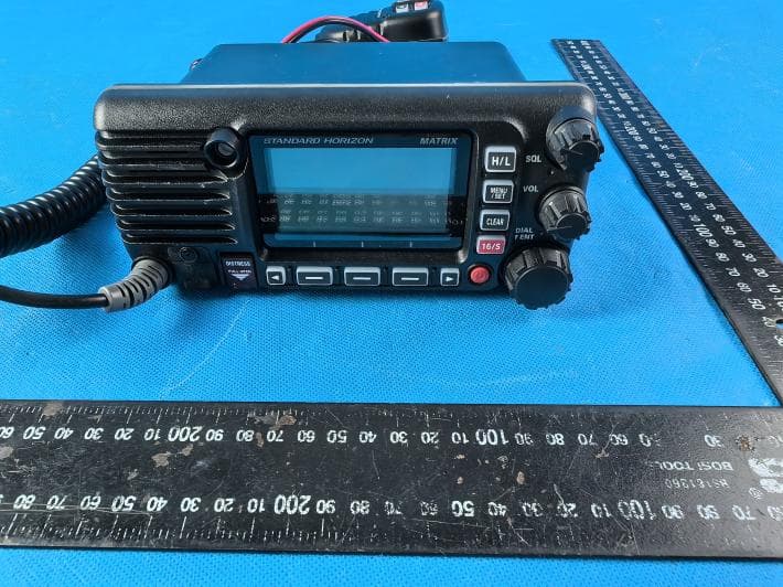
K6630673Y3D
Aug 01, 2024VHF FM Marine Transceiver
Equipment Class
CXX - Communications Rcvr for use w/ licensed Tx and CBs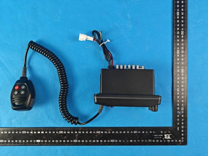
K6630653Y3D
Aug 01, 2024VHF FM Marine Transceiver
Equipment Class
CXX - Communications Rcvr for use w/ licensed Tx and CBs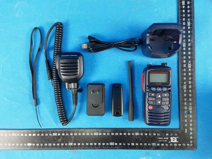
K6630683X30
Jan 10, 2023VHF FM Marine Transceiver
Equipment Class
TNF - Licensed Non-Broadcast Transmitter Held to Face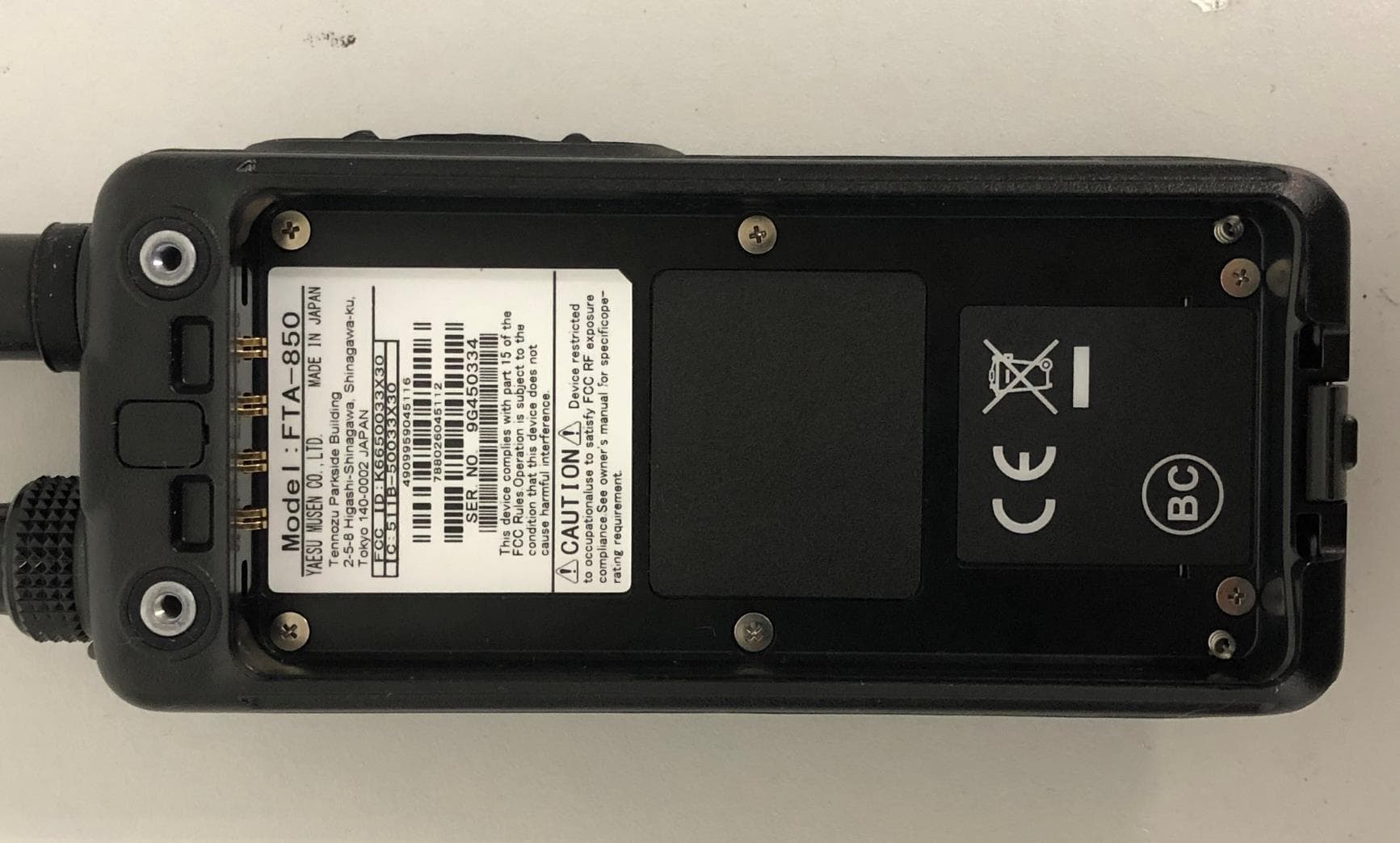
K6650033X30
Nov 18, 2020Airband Radio Transceiver
Equipment Class
TNF - Licensed Non-Broadcast Transmitter Held to Face