K6630283X3SMARINE TRANSCEIVER
Yaesu Musen Co., Ltd.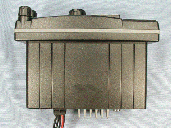
Click to zoom
Application Details
- Equipment Class
- TNB - Licensed Non-Broadcast Station Transmitter
- Date of Grant
- Mar 08, 2007
- Application Purpose
- Original Equipment
- Date of Application
- Mar 08, 2007
- Equipment Note
- MARINE TRANSCEIVER
- Frequency Range
- 156.52500000 - 156.52500000
- Company
- Yaesu Musen Co., Ltd.
- Country
- Japan
Documents & Files
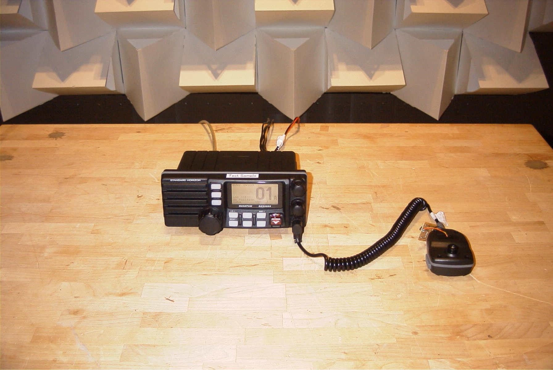
Document Text
Text extracted from the exhibit documents filed with the FCC. Open a document above to read the original.
Users Manual
FCC ID: K6630283X3S IC ID: 511B-30283X3S GX5000S / GX5500S Operating Manual • Waterproof construction • Independent Channel 70 receiver built-in for continuous DSC watching • 30 W Loud Hailer with listen back and 4 fog horns, Bells & Whistles • Capable of connecting 2 optional enhanced CMP25 RAM+ second station remote microphone or VH-310 Handset • Intercom between radio and second station microphone • DSC position request and send functions with compatible STANDARD HORIZON GPS Chart plotters • Versatile user-programmable scanning, priority scan and Dual Watch • One-button access to Channel 16 and 9 • Oversized rotary channel knob, backlit display and keys. • Navigation information shown on display when optional GPS connected • Unique Receive Audio Tone Control TABLE OF CONTENTS 1 GENERAL INFORMATION 2 PACKING LIST 3 OPTIONS 4 SAFETY / WARNING INFORMATION 5 FCC RADIO LICENSE INFORMATION 6 FCC NOTICE 7 GETTING STARTED 7.1 ABOUT VHF RADIO 7.2 SELECTING AN ANTENNA 7.3 COAXIAL CABLE 8 INSTALLATION 8.1 LOCATION 8.2 MOUNTING THE RADIO 8.2.1 Supplied Universal Mounting Bracket 8.2.2 Optional MMB-84 Flush Mount Bracket 8.3 ELECTRICAL CONNECTIONS 8.4 ACCESSORY CABLE 8.5 CHECKING GPS CONNECTIONS 8.6 CHANGING THE GPS TIME 8.7 CHANGING THE TIME LOCATION 8.8 CHANGING COG TO TRUE OR MAGNETIC 8.9 RECEIVER AUDIO TONE CONTROL 8.10 OPTIONAL ENHANCED RAM+ SECOND STATION MIC AND/OR VH-310 HANDSET INSTALLATION 9 CONTROLS AND INDICATORS 10 BASIC OPERATION 10.1 RECEPTION 10.2 TRANSMISSION 10.3 TRANSMIT TIME-OUT TIMER (TOT) 10.4 SIMPLEX / DUPLEX CHANNEL USE 10.5 USA, CANADA, AND INTERNATIONAL MODE 10.6 NOAA WEATHER CHANNELS 10.6.1 NOAA Weather Alert Vertex Standard Co., Ltd. 1 FCC ID: K6630283X3S IC ID: 511B-30283X3S GX5000S / GX5500S Operating Manual 10.6.2 NOAA Weather Alert Testing 10.7 EMERGENCY (CHANNEL 16 USE) 10.8 CALLING ANOTHER VESSEL (CHANNEL 16 OR 9) 10.9 MAKING TELEPHONE CALLS 10.10 OPERATING ON CHANNELS 13 AND 67 10.11 DUAL WATCH (TO PRIORITY CHANNEL) 10.12 SCANNING 10.12.1 Selecting the Scan Mode 10.12.2 Memory Scanning (M-SCAN) 10.12.3 Priority Scanning (P-SCAN) 10.13 FOG / PA OPERATION 10.13.1 Operating the PA HAIL mode 10.13.2 Operating the FOG HORN mode 10.14 NAVIGATION INDICATION 10.15 INTERCOM OPERATION 10.15.1 Communication 10.15.2 Calling 10.16 VOICE SCRAMBLER 11 DIGITAL SELECTIVE CALLING 11.1 GENERAL 11.2 MARITIME MOBILE SERVICE IDENTITY (MMSI) 11.2.1 what is an MMSI? 11.2.2 Programming the MMSI 11.3 DSC DISTRESS ALERT 11.3.1 Transmitting a DSC Distress Alert 11.3.2 Receiving a DSC Distress Alert 11.3.3 Distress Relay 11.4 ALL SHIPS CALL 11.4.1 Transmitting an All Ships Call 11.4.2 Receiving an All Ships Call 11.5 INDIVIDUAL CALL 11.5.1 Setting up the Individual / Position Call Directory 11.5.2 Setting up Individual Ringer 11.5.3 Setting up Individual / Group Call Ringer 11.5.4 Transmitting an Individual Call 11.5.5 Receiving an Individual Call 11.6 CALL WAITING DIRECTORY 11.6.1 Enabling the Call Waiting Feature 11.6.2 Reviewing Received Calls Logged into the Call Waiting Directory 11.6.3 To Delete the Received Log From the “DSC Log” Directory 11.7 GROUP CALL 11.7.1 Setting up a Group Call 11.7.2 Transmitting a Group Call 11.7.3 Receiving a Group Call 11.8 POSITION REQUEST 11.8.1 Setting up Position Reply 11.8.2 Transmitting a Position Request to Another Vessel 11.8.3 Receiving a Position Request 11.9 POSITION SEND 11.8.1 Setting up Position Send Ringer 11.8.2 Transmitting a DSC Position Send Call 11.8.3 Receiving a DSC Position Send Call 11.10 DSC TRANSMISSION TEST 11.11 MANUAL INPUTTING GPS LOCATION (LAT/LON) Vertex Standard Co., Ltd. 2 FCC ID: K6630283X3S IC ID: 511B-30283X3S GX5000S / GX5500S Operating Manual 12 RADIO SETUP MODE 12.1 LAMP ADJUSTING 12.2 LCD CONTRAST 12.3 TIME OFFSET 12.4 TIME LOCATION 12.5 TRUE MAGNETIC CHANGE (NAV display) 12.6 PRIORITY CHANNEL SET 12.7 SCAN TYPE 12.8 SCAN RESUME TIME 12.9 KEY BEEP (ON/OFF) 12.10 WX ALERT 12.11 VOICE SCRAMBLER 12.12 CHANNEL NAME CHANGE 12.13 NAMING THE RADIO OR SECOND STATION MIC OR HANDSET 12.14 FOG ALERT TONE FREQUENCY 12.15 RECEIVER AUDIO TONE CONTROL 13 ENHANCED RAM+ MIC OPERATION 13.1 RAM+ MIC CONTROLS 13.2 FOG / PA OPERATION 13.2.1 Operating the PA / HAIL mode 13.2.2 Operating the FOG HORN mode 13.3 INTERCOM OPERATION 13.3.1 Communication 13.3.2 Calling 13.4 MANUAL INPUTTING OF THE GPS LOCATION (LAT/LON) 13.5 DSC / RADIO SETUP MODE 13.5.1 Changing GPS Information to Vessel Position or COG 14 VH-310 HANDSET OPERATION 14.1 VH-310 HANDSET CONTROLS 14.2 FOG / PA OPERATION 14.2.1 Operating the PA HAIL mode 14.2.2 Operating the FOG HORN mode 14.3 INTERCOM OPERATION 14.3.1 Communication 14.3.2 Calling 14.4 MANUAL INPUTTING OF THE GPS LOCATION (LAT/LON) 14.5 DSC / RADIO SETUP MODE 14.5.1 Changing GPS Information to Vessel position or COG 14.5.2 External Speaker AF Selection 15 FOG HORN TIMING CHART 16 MAINTENANCE 16.1 REPLACEMENT PARTS 16.2 FACTORY SERVICE 16.3 TROUBLESHOOTING CHART 17 CHANNEL ASSIGNMENTS 18 SPECIFICATIONS 19 APPENDIX Vertex Standard Co., Ltd. 3 FCC ID: K6630283X3S IC ID: 511B-30283X3S GX5000S / GX5500S Operating Manual 1 GENERAL INFORMATION The Vertex Standard GX5000S/GX5500S are a VHF/FM transceiver designed for use in the frequency range of 156.025 to 163.275 MHz. The GX5000S/GX5500S can be operated from 11 to 16 VDC and has a switchable RF output power of 1 watt or 25 watts. The GX5000S/GX5500S are a Class D DSC (Digital Selective Calling) VHF and includes a 30W PA with preprogrammed fog signals, bells and whistles. 2 connections are available for the RAM+ or VH-310 second station remote microphones. Class D operation allows continuous receiving of Digital Selective Calling functions on channel 70 even if the radio is receiving a call. 2 PACKING LIST When the package containing the transceiver is first opened, please check it for the following contents: GX5000S or GX5500S Transceiver Mounting Bracket and mounting hardware Power Cord Owner’s Manual Warranty Card 3 OPTIONS MMB-84 Flush-Mount Bracket CMP25B/W Remote-A…
Text truncated - open the document above for the full version.
Attestation Statements
TIMCO ENGINEERING INC. 849 NW State Road 45 Newberry, Florida 32669 http://www.timcoengr.com 888.472.2424 F 352.472.2030 email: [email protected] APPLICANT: VERTEX STANDARD CO., LTD. FCC ID: K6630283X3S REPORT #: W:\V\VERTEX\361AUT7\361AUT7 Compliance Verification.doc TECHNICAL DATA: 80.203 (b) External Controls: The transmitter is capable of changing frequency between 156.05 – 157.425 MHz by external control. The available channels are shown in the User Manual description Channel List. These channels are preprogrammed by the manufacturer and change of frequency is inaccessible to the station operator. 80.203 (c) Five minutes continuous transmission test. The antenna was connected to a dummy load and the radio was locked in a transmit PTT mode. An external timer digital clock was used to observe the duration of the un-modulated transmission. The transmitter turned off and the radio went to receive mode at 4 minutes, 58 seconds as displayed by the external digital clock. 80.203 (n) This radio complies with the requirement for DSC capability in the 156 – 162 MHz band and in accordance with 80.225. 80.873; 80.956 Transmitter G3E emission capability: The transmitter was connected to 50 ohm resistive wattmeter and the frequency was set to 156.300 and to 156.800 MHz. With normal modulation, the output power displayed was 25 Watts at the high power setting and 1 watt at low power setting, consistent with previous measurements. The transmitter has been demonstrated to be capable, with normal operating voltages applied, of delivering 25 watts of carrier power into a 50 ohm resistive load over the specified frequencies. 80.911 (a) 80.956 G3E Transmissions: This radio is capable of G3E emission on 156.300 and 156.800 MHz 80.911 (c) With 13.6 VDC applied and with the radio connected to a 50 ohm resistive wattmeter, the output power was measured at 156.300 and 156.800 MHz with a measured reading of 25 Watts under normal speech modulation. 80.911 (d)(2) 80.959 With the power supply set to 13.6 VDC, and the output of the transmitter terminated in a 50 ohm matching artificial load, the transmitter output power was monitored over a 10 minute continuous operational period while in full power. The output power varied from the nominal 25 Watts output power to 24.8 Watts output power
Attestation Statements
January 29, 2007 Federal Communications Commission Authorization and Evaluation Division, 7435 Oakland Mills Road Columbia, MD 21046 USA Re: GX5000S and GX5500S (FCC ID: K6630283X3S) Gentlemen: A. Part 15.21 Compliance Statement Drawing: Unauthorized changes or modifications to this equipment may void com- pliance with FCC Rules. Any change or modification must be approved in writing by STANDARD HORIZON. 20mm 97mm B. Part 15.21 Compliance Statement Drawing Location: IN OPERATION MANUAL (location on Page 7) Sincerely, Vertex Standard Co., Ltd. Mr. Moto Kurihara Group Leader of Engineering Division
Cover Letter(s)
January 29, 2007 Federal Communications Commission EQUIPMENT APPROVAL SERVICES P. O. Box 358315 Pittsburgh, PA 15251-5315 Attention: Authorization and Evaluation Division Reference: GX5000S and GX5500S (FCC ID: K6630283X3S) Pursuant to Sections 0.457 (d)(1)(ii) and 0.459 of the Commission’s Rules, the Applicant hereby requires confidential treatment of some of the information accompanying this Application, as listed below: ・ Block Diagram ・ Schematics These materials contain trade secrets and proprietary information not customarily released to the public. The public disclosure of these matters might be harmful to the Applicant and provide unjustified benefits to its competitors. The Applicant understands that pursuant to Rule 0.457 (d)(1)(ii), disclosure of the Application and all accompanying documentation will not be made before the date of Grant for this Application. Sincerely, Vertex Standard Co., Ltd. Mr. Moto Kurihara Group Leader of Engineering Division
External Photos
FCC ID: K6630283X3S IC ID: 511B-30283X3S Vertex Standard Co., Ltd. Front view (GX5000S) Front view (GX5500S) FCC ID: K6630283X3S IC ID: 511B-30283X3S Vertex Standard Co., Ltd. Rear view (GX5000S) Rear view (GX5500S) FCC ID: K6630283X3S IC ID: 511B-30283X3S Vertex Standard Co., Ltd. Left side view Right side view FCC ID: K6630283X3S IC ID: 511B-30283X3S Vertex Standard Co., Ltd. Top view Bottom view FCC ID: K6630283X3S IC ID: 511B-30283X3S Vertex Standard Co., Ltd. Microphone DC Cable
ID Label/Location Info
GX5000S/GX5500SGX5000S/GX5500S LABEL DRAWINGLABEL DRAWING Vertex Standard Co., Ltd.Vertex Standard Co., Ltd. ID / Part 15.19 and CAUTION drawings ID drawing Part 15.19 and CAUTION drawings Label location This device complies with part 15 of the FCC Rules. Operation is subject to the condition that this device does not cause harmful interference. Device restricted to occupational use to satisfy FCC RF exposure compliance. See owners manual for specific operating requirement. ! ! CAUTION GX5000S VERTEX STANDARD CO., LTD. MADE IN JAPAN IC: 511B-30283X3S FCC ID: K6630283X3S 4909959000000 SER NO. 00000000 GX5500S VERTEX STANDARD CO., LTD. MADE IN JAPAN IC: 511B-30283X3S FCC ID: K6630283X3S 4909959000000 SER NO. 00000000
Internal Photos
FCC ID: K6630283X3S IC ID: 511B-30283X3S Vertex Standard Co., Ltd. Top of EUT without case Bottom of EUT without case FCC ID: K6630283X3S IC ID: 511B-30283X3S Vertex Standard Co., Ltd. Side-A of MAIN-UNIT with shield cases Side-A of MAIN-UNIT without shield cases FCC ID: K6630283X3S IC ID: 511B-30283X3S Vertex Standard Co., Ltd. Side-B of MAIN-UNIT Side-A of SUB-UNIT with shield cases FCC ID: K6630283X3S IC ID: 511B-30283X3S Vertex Standard Co., Ltd. Side-A of SUB-UNIT without shield cases Side-B of SUB-UNIT FCC ID: K6630283X3S IC ID: 511B-30283X3S Vertex Standard Co., Ltd. Side-A of CNTL-1-UNIT with LCD (GX5000S) Side-A of CNTL-1-UNIT without LCD (GX5000S) FCC ID: K6630283X3S IC ID: 511B-30283X3S Vertex Standard Co., Ltd. Side-B of CNTL-1-UNIT (GX5000S) Side-A of CNTL-2-UNIT with LCD (GX5500S) FCC ID: K6630283X3S IC ID: 511B-30283X3S Vertex Standard Co., Ltd. Side-A of CNTL-2-UNIT without LCD (GX5500S) Side-B of CNTL-2-UNIT (GX5500S) FCC ID: K6630283X3S IC ID: 511B-30283X3S Vertex Standard Co., Ltd. Front of LCD Rear of LCD FCC ID: K6630283X3S IC ID: 511B-30283X3S Vertex Standard Co., Ltd. Side-A of –CONNECTOR-UNIT Side-B of CONNECTOR-UNIT FCC ID: K6630283X3S IC ID: 511B-30283X3S Vertex Standard Co., Ltd. Side-A of TERMINAL-UNIT (GX5000S)/TERMINA-2-UNIT (GX5500S) Side-B of TERMINAL-UNIT (GX5000S)/TERMINA-2-UNIT (GX5500S) FCC ID: K6630283X3S IC ID: 511B-30283X3S Vertex Standard Co., Ltd. Top of chassis Bottom of chassis FCC ID: K6630283X3S IC ID: 511B-30283X3S Vertex Standard Co., Ltd. Inside of panel (GX5000S) Inside of panel (GX5500S) FCC ID: K6630283X3S IC ID: 511B-30283X3S Vertex Standard Co., Ltd. Inside of microphone (1) Inside of microphone (2)
Parts List/Tune Up Info
FCC ID: K6630283X3S IC ID: 511B-30283X3S Alignment GX5000S/GX5500S Alignment The GX5000S/GX5500S has been carefully aligned at the factory for the specified performance across the marine band. Realignment should therefore not be necessary except in the event of a component failure. All component replacement and service should be performed only by an authorized Standard Horizon representative, or the warranty policy may be voided. The following procedures cover the sometimes critical and tedious adjustments that are not normally required once the transceiver has left the factory. However, if damage occurs and some parts are replaced, realignment may be required. If a sudden problem occurs during normal operation, it is likely due to component failure; realignment should not be done until after the faulty component has been replaced. We recommend that servicing be performed only by authorized Standard Horizon service technicians who are experienced with the circuitry and fully equipped for repair and alignment. Therefore, if a fault is suspected, contact the dealer from whom the transceiver was purchased for instructions regarding repair. Authorized Standard Horizon service technicians realign all circuits and make complete performance checks to ensure compliance with factory specifications after replacing any faulty components. Those who do undertake any of the following alignments are cautioned to proceed at their own risk. Problems caused by unauthorized attempts at realignment are not covered by the warranty policy. Also, Standard Horizon, a division of VERTEX STANDARD, must reserve the right to change circuits and alignment procedures in the interest of improved performance, without notifying owners. Under no circumstances should any alignment be attempted unless the normal function and operation of the transceiver are clearly understood, the cause of the malfunction has been clearly pinpointed and any faulty components replaced, and the need for realignment determined to be absolutely necessary. The following test equipment (and thorough familiarity with its correct use) is necessary for complete realignment. Correction of problems caused by misalignment resulting from use of improper test equipment is not covered under the warranty policy. While most steps do not require all of the equipment listed, the interactions of some adjustments may require that more complex adjustments be performed afterwards. Do not attempt to perform only a single step unless it is clearly isolated electrically from all other steps. Have all test equipment ready before beginning, and follow all of the steps in a section in the order presented. 1/7 Vertex Standard Co., Ltd. FCC ID: K6630283X3S IC ID: 511B-30283X3S Alignment Required Test Equipment RF Signal Generator with calibrated output level at 200 MHz Deviation Meter (linear detector) AF Millivoltmeter SINAD Meter Inline Wattmeter with 5% accuracy at 200 MHz Regulated DC Power Supply: 13.8 VDC, 10A 50-ohm Non-reactive Dummy Load: 30W at 200 MHz Frequency Counter: >0.1 ppm accuracy at 200 MHz AF Signal Generator DC Voltmeter: high impedance VHF Sampling Coupler AF Dummy Load: 4 Ohms, 10 W Oscilloscope Spectrum Analyzer GX3500S Marine Transceiver Alignment Preparation & Precautions A dummy load and inline wattmeter must be connected to the main antenna jack in all procedures that call for transmission. Correct alignment is not possible with an antenna. After completing one step, read the following step to determine whether the same test equipment will be required. If not, remove the test equipment (except dummy load and wattmeter, if connected) before proceeding. Correct alignment requires that the ambient temperature be the same as that of the transceiver and test equipment, and that this temperature be held constant between 20°C and 30°C (68°F and 86°F). When the transceiver is brought into the shop from hot or cold air it should be allowed some time for thermal equalization with the environment before alignment. If possible, alignments should be made with oscillator shields and circuit boards firmly affixed in place. Also, the test equipment must be thoroughly warmed up before beginning. Note: Signal levels in dB referred to in this procedure are based on 0 dBμ = 0.5 μV (closed circuit). Overview of Test Mode The test mode has been built in the microprocessor in order to adjust and confirm the performance of transceiver. The purpose is to adjust transceiver simply and to confirm the performance of transceiver smoothly. 2/7 Vertex Standard Co., Ltd. FCC ID: K6630283X3S IC ID: 511B-30283X3S Alignment (A) In CH70, every time you are in transmit mode, (every time you press PTT), the following test tone can be outputted: 1st transmission: Synthetic tone of 1300 Hz and 2100 Hz 2nd transmission: 1300 Hz 3rd transmission: 2100 Hz 4th transmission: No modulation 5th transmission: Return to 1st transmission (B) Scan the channels between WX10 and EXP04 in the SCAN mode. Starting Test Mode Confirm that PWR/VOL switch is off, and short the TEST points (JP1001). Turn on the PWR/VOL switch while press and holding the [DISTRESS] and [DW (IC)] keys. Adjustment of Main PLL Frequency Adjust the frequency in the transmit mode and local frequency in the receive mode. Connect the frequency counter to the antenna jack. Set the channel to CH16. With the PTT switch pressed, adjust TC1001 so that RF frequency is 156.80000 MHz ± 100 Hz. Adjustment of Sub PLL Frequency Adjust the frequency of the ch70 receiver. Connect the frequency counter to the test point TP4004. Adjust TC4001 so that RF frequency is 134.225 MHz ± 100Hz. Adjustment of VCO Connect the DC voltmeter to the test point (LOCK TP). Use the 16/9 key to set the channel to CH16, adjust TC1002 so that voltage on the TP1008 is 1.5 V ±0.1 V in the receive mode. Adjustment and Confirmation of Transmit Power Adjust power at high and low in the transmit mode, and confirm power in the…
Text truncated - open the document above for the full version.
Parts List/Tune Up Info
1 FCC ID: K6630283X3S/IC ID: 511B-30283X3S GX5000S/GX5500SSemi-Conductor Parts List Address Parts Code Device NameDescriptionTYP VAL MAIN-UNIT D 1001 Q9000586 Surge Absorber DSP-141N-S00B D 1002 G2090778 Diode1N5402 D 1003 G2070076 Diode1SS321 D 1004 G2090792 DiodeL308CCB D 1005 G2090792 DiodeL308CCB D 1006 G2070118 DiodeHSU277 D 1007 G2070118 DiodeHSU277 D 1008 G2070176 DiodeDAN235U D 1009 G2070452 DiodeHVU359 D 1010 G2070754 Zener DiodeHZU5ALL-E D 1011 G2070088 Diode1SS302 D 1012 G2070918 DiodeHVC306B D 1013 G2070918 DiodeHVC306B D 1014 G2070918 DiodeHVC306B D 1015 G2070918 DiodeHVC306B D 1016 G2070918 DiodeHVC306B D 1017 G2070918 DiodeHVC306B D 1018 G2070910 Zener DiodeUDZS 5.6B D 1019 G2070178 DiodeDA221 D 1020 G2070178 DiodeDA221 Q 1001 G3213017Q Transistor2SB1301 ZQ/ZP Q 1002 G3213017Q Transistor2SB1301 ZQ/ZP Q 1003 G3213017Q Transistor2SB1301 ZQ/ZP Q 1004 G1093640 ICNJM7808FA Q 1005 G3070074 TransistorDTA144EE Q 1006 G3070247 TransistorRT1N441U-1 Q 1007 G3070247 TransistorRT1N441U-1 Q 1008 G3070247 TransistorRT1N441U-1 Q 1009 G3070247 TransistorRT1N441U-1 Q 1010 G1093695 PWR-MODULE RA35H1516M Q 1011 G3070247 TransistorRT1N441U-1 Q 1012 G1093660 ICNJM78M05DL1A Q 1013 G4802948 FET3SK294 Q 1014 G3070022 TransistorDTB123EK Q 1015 G3070022 TransistorDTB123EK Q 1016 G3070247 TransistorRT1N441U-1 Q 1017 G3333567E Transistor2SC3356 R25 Q 1018 G3070247 TransistorRT1N441U-1 Q 1019 G3070247 TransistorRT1N441U-1 Q 1020 G3070247 TransistorRT1N441U-1 Q 1021 G3341548E Transistor2SC4154-1E Q 1022 G3341548E Transistor2SC4154-1E Q 1023 G3341548E Transistor2SC4154-1E Q 1024 G3333567E Transistor2SC3356 R25 Q 1025 G3116028F Transistor2SA1602A-1F Q 1026 G1092541 ICMB15A02PFV1-G-BND-EFE1 Q 1027 G3070247 TransistorRT1N441U-1 Q 1028 G1094009 ICLM2902PWR Q 1029 G3805207A FET2SK520 K41 Q 1030 G3805207A FET2SK520 K41 Q 1031 G3350068 Transistor2SC5006 Q 1032 G3070247 TransistorRT1N441U-1 Q 1033 G3805207A FET2SK520 K41 Vertex Standard Co.,Ltd. 2 FCC ID: K6630283X3S/IC ID: 511B-30283X3S GX5000S/GX5500SSemi-Conductor Parts List Address Parts Code Device NameDescriptionTYP VAL Q 1034 G1094010 ICLM2904PWR Q 1035 G3805207A FET2SK520 K41 Q 1036 G3070247 TransistorRT1N441U-1 Q 1037 G3111627G Transistor2SA1162GR Q 1038 G3327127G Transistor2SC2712GR Q 1039 G3805207C FET2SK520 K43 Q 1040 G3350068 Transistor2SC5006 Q 1041 G3344008C Transistor2SC4400-3 Q 1042 G1093864 ICCD4053BPWR Q 1044 G1094102 ICM62421FP Q 1045 G1094009 ICLM2902PWR Q 1046 G3344008C Transistor2SC4400-3 Q 1047 G1091605 ICTA31136FNG Q 1048 G3341548E Transistor2SC4154-1E Q 1049 G3341548E Transistor2SC4154-1E Q 1050 G3341548E Transistor2SC4154-1E Q 1051 G1093865 ICCD4066BPWR Q 1052 G3341548E Transistor2SC4154-1E Q 1053 G1092943 ICNJM2211M Q 1054 G3070247 TransistorRT1N441U-1 Q 1055 G1092241 ICLA4425A Q 1056 G1094010 ICLM2904PWR Q 1057 G1093865 ICCD4066BPWR CNTL-1-UNITGX5000S D 2001 G2070702 DiodeMC2846-1 D 2002 G2070916 LEDFY1111C-722 D 2003 G2070916 LEDFY1111C-722 D 2004 G2070916 LEDFY1111C-722 D 2005 G2070916 LEDFY1111C-722 D 2006 G2070916 LEDFY1111C-722 D 2007 G2070916 LEDFY1111C-722 D 2008 G2070916 LEDFY1111C-722 D 2009 G2070916 LEDFY1111C-722 D 2010 G2070916 LEDFY1111C-722 D 2011 G2070916 LEDFY1111C-722 D 2012 G2070916 LEDFY1111C-722 D 2013 G2070916 LEDFY1111C-722 D 2014 G2070916 LEDFY1111C-722 D 2015 G2070916 LEDFY1111C-722 D 2016 G2070916 LEDFY1111C-722 D 2017 G2070916 LEDFY1111C-722 D 2020 G2070530 Zener DiodeHZM27WA D 2021 G2070530 Zener DiodeHZM27WA D 2022 G2070530 Zener DiodeHZM27WA D 2023 G2070530 Zener DiodeHZM27WA D 2024 G2070470 Diode1SS355 D 2025 G2070078 DiodeIMN10 D 2026 G2070078 DiodeIMN10 D 2027 G2070474 DiodeD1F20-5063 D 2028 G2070470 Diode1SS355 D 2029 G2070470 Diode1SS355 D 2030 G2070752 DiodeRB715F D 2032 G2070470 Diode1SS355 Vertex Standard Co.,Ltd. 3 FCC ID: K6630283X3S/IC ID: 511B-30283X3S GX5000S/GX5500SSemi-Conductor Parts List Address Parts Code Device NameDescriptionTYP VAL DS2001 Q7000588 LCD ModuleGX5000S Q 2001 G1094438 ICM30873FHAGP Q 2002 G1094009 ICLM2902PWR Q 2003 G1094258 ICSN74LVC3G14DC Q 2004 G1094227 ICSN74HC14APW Q 2005 G3070247 TransistorRT1N441U-1 Q 2006 G1094229 ICUA78L05ACPKE6 Q 2007 G1093635 ICS-80823CNMC-B8I Q 2008 G3070248 TransistorRT1P441U-1 Q 2009 G1094409 ICM24256-BWDW6 Q 2010 G1094056 ICS-812C33AUA-C2N Q 2011 G3341548E Transistor2SC4154-1E Q 2012 G3211327R Transistor2SB1132 R Q 2013 G1094430 ICSN74LVC4245APWR Q 2014 G1093870 ICSN74LV4053APWR Q 2015 G3116028F Transistor2SA1602A-1F Q 2016 G3341548E Transistor2SC4154-1E Q 2017 G3116028F Transistor2SA1602A-1F Q 2018 G3341548E Transistor2SC4154-1E Q 2019 G3116028F Transistor2SA1602A-1F Q 2020 G3341548E Transistor2SC4154-1E Q 2021 G3341548E Transistor2SC4154-1E Q 2022 G3070247 TransistorRT1N441U-1 Q 2023 G0090037 PhotocouplerTLP281 Q 2024 G1094229 ICUA78L05ACPKE6 Q 2025 G3070084 TransistorDTC114EUA Q 2028 G1094439 ICS-35390A Q 2029 G3070084 Transisto rDTC114EUA CNTL-2-UNITGX5500S D 3001 G2070702 DiodeMC2846-1 D 3002 G2070078 DiodeIMN10 D 3003 G2070078 DiodeIMN10 D 3004 G2070916 LEDFY1111C-722 D 3005 G2070916 LEDFY1111C-722 D 3006 G2070916 LEDFY1111C-722 D 3007 G2070916 LEDFY1111C-722 D 3008 G2070916 LEDFY1111C-722 D 3009 G2070916 LEDFY1111C-722 D 3010 G2070916 LEDFY1111C-722 D 3011 G2070916 LEDFY1111C-722 D 3012 G2070916 LEDFY1111C-722 D 3013 G2070916 LEDFY1111C-722 D 3014 G2070916 LEDFY1111C-722 D 3015 G2070916 LEDFY1111C-722 D 3016 G2070916 LEDFY1111C-722 D 3017 G2070916 LEDFY1111C-722 D 3018 G2070916 LEDFY1111C-722 D 3019 G2070916 LEDFY1111C-722 D 3022 G2070530 Zener DiodeHZM27WA D 3023 G2070530 Zener DiodeHZM27WA D 3024 G2070530 Zener DiodeHZM27WA D 3025 G2070530 Zener DiodeHZM27WA D 3026 G2070470 Diode1SS355 Vertex Standard Co.,Ltd. 4 FCC ID: K6630283X3S/IC ID: 511B-30283X3S GX5000S/GX5500SSemi-Conductor Parts List Address Parts Code Device NameDescriptionTYP VAL D 3027 G2070474 DiodeD1F20-5063 D 3028 G2070470 Diode1SS355 D 3029 G2070470 Diode1SS355 D 3030 G2070470 Diode1SS355 D 3032 G2070752 DiodeRB715F DS3001 Q7000589 LCD ModuleGX5500S Q 3001 G3070247 …
Text truncated - open the document above for the full version.
RF Exposure Info
3/5/2007 Page 1 of 3 FCC ID: K6630283X3S FCC RF Exposure Requirements General information : FCC ID: K6630283X3S Device category: Mobile per Part 2.1091 Environment: Uncontrolled Exposure Mobile devices that operate under Part 80 of this chapter are subject to routine environmental evaluation for RF exposure prior to equipment authorization or use if they operate at frequencies of 1.5 GHz or below and their effective radiated power (ERP) is 1.5 watts or more. However, compliance with the power density limits of 1.1310 is not required. Antenna: The manufacturer does specify an antenna with a gain of 3 dBi to be used with this device. This device has provisions for operation in a vehicle, or a fixed location. Configuration Antenna p/n Type Max. Gain (dBi) Boat Any omni 3 Operating configuration and exposure conditions: The conducted output power is 25 Watts. Typical use qualifies for a maximum duty cycle factor of 50%. The manufacturer also markets this device only for occupation use. - Part 2.1091 states that devices are excluded from routine evaluation if the EIRP is less than 2.46Watt (or 1.5WERP). - Vehicle Operation: The maximum antenna gain that can be used is 3dBi. A coaxial cable of the type RG 58 has a loss of 1dB for a length of 15 feet. MPE Calculation: The minimum separation distance is calculated as follows: The limit for occupation/controlled exposure environment below 300 MHz is .2 mW/cm 2 . 3/5/2007 Page 2 of 3 FCC ID: K6630283X3S Channel frequency: 156.025-157.425 MHz The conducted power output is 25 watt. The coax loss was taken as 1 dB. Antenna gain was taken as 3 dBi 50% talk time in 30 minutes S f 1500 := power density limit for controlled exposure G1dBd2.15+:= gain in dBi G13=dBi S0.2= CL1:= dB coax loss GG1CL−:= gain numeric Gn10 G 10 := Gn1.585=dB R Po Gn⋅() 4π⋅S⋅ () := inches R 2.54 := R88.784= distance in centimeters required for compliance inches34.954= W25:= power in Watts D1:= Duty Factor in decimal % (1=100%) 1 for FM E15:= exposure time in minutes U30:= (use 6 for controlled and 30 for uncontrolled ) WexpW D⋅ E U ⎛ ⎜ ⎝ ⎞ ⎠ ⋅:= PC E U ⎛ ⎜ ⎝ ⎞ ⎠ 100⋅:= Wexp12.5=WattsPC50= % on time Po12500:=mWatts f300:= Frequency in MHz dBd.85:= antenna gain in dBd 3/5/2007 Page 3 of 3 FCC ID: K6630283X3S Conclusion: The device complies with the MPE requirements by providing a safe separation distance of 0.89m between the antenna, including any radiating structure, and any persons when normally operated . Proposed RF exposure safety information to include in User’s Manual : “FCC RF Exposure Requirements: CAUTION: The antenna(s) used for this transmitter must not be co-located or operating in conjunction with any other antenna or transmitter. This device is approved with emissions having a source-based time- averaging duty factor not exceeding 50%. Failure to observe these restrictions will result in exceeding the FCC RF exposure limits.
Test Report
Page 1 of 35 REPORT ON Radio testing of the STANDARD HORIZON GX5000S In accordance with ANSI/TIA/EIA-603, RSS-182 January 200 7Report number TA000448 Vertex Standard Co., Ltd. GENERAL INFORMATION TRANSMITTERS x Switchable Variable N/ A RECEIVERS This re port was prepared by Vertex Standard Co., Ltd. 4.8[A] Collector Voltage:13.8[V] 50 2000 69 DC 65 ANSI/TIA/EIA-603 50 156.050 to163.425 50 1st 2nd Date 25 / January /200 7 Test performed by M.Kurihara INPUT IMPEDANCE (MIC): MAXIMUM POWER RATING: INPUT IMPEDANCE (RF): INTERMEDIATE FREQUENCIES: FREQUENCY RANGE: OUTPUT IMPEDANCE (RF): OUTPUT IMPEDANCE (RF): Collector Current: [V] GX5000S K6630283X3 S STANDARD HORIZON 511B-30283X3 S [W]AUDIO OUTPUT POWER: OUTPUT IMPEDANCE (SP):[Ω]4 4.5 [Ω] [MHz] [kHz] -30.4 -450 [MHz] [W] [Ω] [Ω] [Ω] [MHz] [W] 16K0G3E, 16K0G2B( for DSC) POWER OUTPUT RATING: 156 1 157.4to to25 TYPE OF EMISSION: FREQUENCY RANGE: RSS-182 VOLTAGE RQUIREMENTS: SERIAL NUMBER: SPECIFICATION ARE REFERENCE D NUMBER OF CHANNELS: FCC ID: TRADE NAME: VHF FM Mobile Transceive rEUT DESCRIPTION: 13.8 7C000001 MANUFACTURER:Vertex Standard Co., Ltd. IC ID: MODEL NAME: Report number TA00044 8Page 2 of 35 Vertex Standard Co., Ltd. GX5000S Channel Settings HILOW 1CH16156.800156.80025k25W1W 2CH70156.525156.52525k25W1W 3 4 5 6 7 8 9 10 11 12 13 14 15 16 17 18 19 20 Report number TA000448Page 3 of 35 Power Transmit Frequency [MHz] CH No. Receive Frequency [MHz] CH Spacing Shown on LCD Vertex Standard Co., Ltd. NAME OF TEST:R.F. Power Output (Conducted) SPECIFICATION:47 CFR 2.1046 (a) GUIDE:ANSI/TIA/EIA-603, Paragraph 2.2.1 TEST EQUIPMENT: As per attached page The EUT was connected to a resistive coaxial attenuator of normal load impedance, and the modulated output powerwas measured by means of an R.F. power meter. Measurement accuracy is ± 4% Report number TA000448Page 4 of 35 24.010 156.525 LOW 1. 2. MEASUREMENT RESULTS 156.800 CHANNEL R.F. POWER, WATTS 16 HIGH NOMINAL, MHz 70 0.803 0.88024.000 MEASUREMENT PROCEDURE Vertex Standard Co., Ltd. Report number TA000448Page 5 of 35 Description (5) Power Supply TEST 1: R.F. POWER OUTPUT TEST 2: FREQUENCY STABILIT Y (4)(3)(1) TRANSMITTER POWER CONDUCTED MEASUREMENTS (5) FREQUENCY COUNTERAgilent 8901B FREQUENCY MODE3026A02806 (3) POWER SENSORAgilent 8482B Serial NumberInstruments Test Sample Agilent 8901B POWE…
Text truncated - open the document above for the full version.
Contact Information
Applicant
Masatoshi Muraishi(Engineering Division)
Test Firm
Timco Engineering, Inc.Sid Sanders
Technical Specifications
| # | Rule Parts | Frequency Range | Power Output | Emission | Tolerance |
|---|---|---|---|---|---|
| 4 | 8 | 156.525 MHz - 156.525 MHz | 1 W | 16K0G2B | 10 ppm |
Other Applications from Yaesu Musen Co., Ltd.
K660E180X10
Dec 01, 2025BLUETOOTH MICROPHONE
Equipment Class
DTS - Digital Transmission System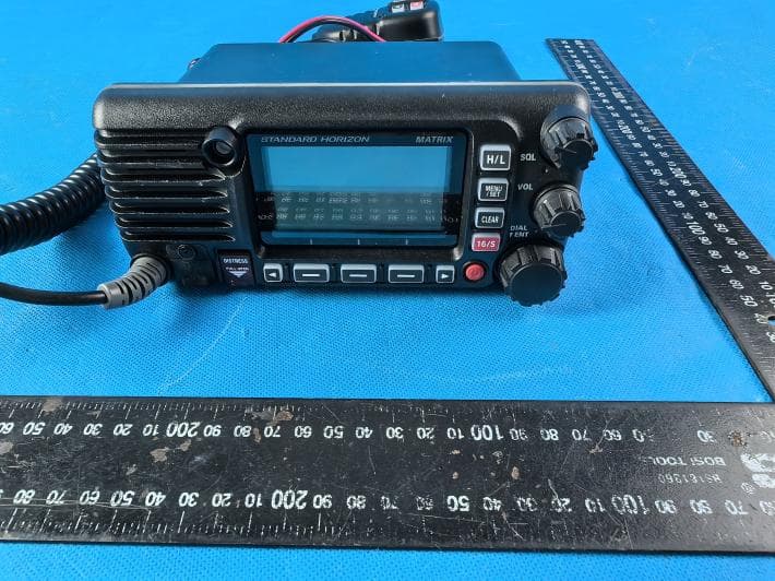
K6630673Y3D
Aug 01, 2024VHF FM Marine Transceiver
Equipment Class
CXX - Communications Rcvr for use w/ licensed Tx and CBs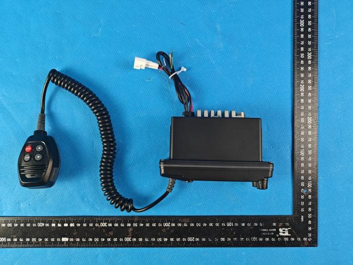
K6630653Y3D
Aug 01, 2024VHF FM Marine Transceiver
Equipment Class
CXX - Communications Rcvr for use w/ licensed Tx and CBs
K6630683X30
Jan 10, 2023VHF FM Marine Transceiver
Equipment Class
TNF - Licensed Non-Broadcast Transmitter Held to Face
K6650033X30
Nov 18, 2020Airband Radio Transceiver
Equipment Class
TNF - Licensed Non-Broadcast Transmitter Held to Face