K6630303X3SMARINE TRANSCEIVER
Yaesu Musen Co., Ltd.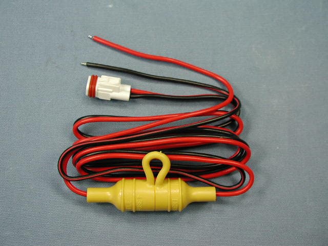
Click to zoom
Application Details
- Equipment Class
- TNB - Licensed Non-Broadcast Station Transmitter
- Date of Grant
- Sep 23, 2007
- Application Purpose
- Original Equipment
- Date of Application
- Sep 20, 2007
- Equipment Note
- MARINE TRANSCEIVER
- Frequency Range
- 156.02500000 - 157.42500000
- Company
- Yaesu Musen Co., Ltd.
- Country
- Japan
Documents & Files
Document Text
Text extracted from the exhibit documents filed with the FCC. Open a document above to read the original.
Users Manual
FCC ID: K6630303X3S IC ID: 511B-30303X3S GX1000S Operating Manual • Compact and Simple Operation • DSC position request and send functions with compatible STANDARD HORIZON GPS Chart plotters • Versatile user-programmable scanning, priority scan and Dual Watch • One-button access to Channel 16 and 9 • Oversized rotary channel knob, backlit display and keys. 1 FCC ID: K6630303X3S IC ID: 511B-30303X3S GX1000S Operating Manual TABLE OF CONTENTS 1 GENERAL INFORMATION 2 PACKING LIST 3 OPTIONS 4 SAFETY / WARNING INFORMATION 5 FCC RADIO LICENSE INFORMATION 6 FCC NOTICE 7 GETTING STARTED 7.1 ABOUT VHF RADIO 7.2 SELECTING AN ANTENNA 7.3 COAXIAL CABLE 8 INSTALLATION 8.1 LOCATION 8.2 ELECTRICAL CONNECTIONS 8.3 ACCESSORY CABLE 8.4 CHECKING GPS CONNECTIONS 8.5 CHANGING THE GPS TIME 8.6 CHANGING THE TIME LOCATION 8.7 OPTIONAL MMB-84 FLUSH MOUNT INSTALLATION 9 CONTROLS AND INDICATORS 10 BASIC OPERATION 10.1 RECEPTION 10.2 TRANSMISSION 10.3 TRANSMIT TIME-OUT TIMER (TOT) 10.4 SIMPLEX / DUPLEX CHANNEL USE 10.5 INTERNATIONAL, USA, AND CANADA MODE 10.6 NOAA WEATHER CHANNELS 2 FCC ID: K6630303X3S IC ID: 511B-30303X3S GX1000S Operating Manual 10.6.1 NOAA Weather Alert 10.6.2 NOAA Weather Alert Testing 10.7 EMERGENCY (CHANNEL 16 USE) 10.8 CALLING ANOTHER VESSEL (CHANNEL 16 OR 9) 10.9 MAKING TELEPHONE CALLS 10.10 OPERATING ON CHANNELS 13 AND 67 10.11 DUAL WATCH (TO PRIORITY CHANNEL) 10.12 SCANNING 10.12.1 Selecting the Scan Mode 10.12.2 Memory Scanning (M-SCAN) 10.12.3 Priority Scanning (P-SCAN) 10.13 NAVIGATION INDICATION 11 DIGITAL SELECTIVE CALLING 11.1 GENERAL 11.2 DSC SCAN 11.3 MARITIME MOBILE SERVICE IDENTITY (MMSI) 11.3.1 what is an MMSI? 11.3.2 Programming the MMSI 11.4 DSC DISTRESS CALL 11.4.1 Transmitting a DSC Distress Call 11.4.2 Receiving a DSC Distress Call 11.5 ALL SHIPS CALL 11.5.1 Transmitting an All Ships Call 11.5.2 Receiving an All Ships Call 11.6 INDIVIDUAL CALL 11.6.1 Setting up the Individual / Position Call Directory 11.6.2 Setting up Individual Reply 3 FCC ID: K6630303X3S IC ID: 511B-30303X3S GX1000S Operating Manual 11.6.3 Setting up Individual / Group Call Ringer 11.6.4 Transmitting an Individual Call 11.6.5 Receiving an Individual Call 11.6.6 Setting Call Waiting Function 11.7 POSITION REQUEST 11.7.1 Setting up Position Reply 11.7.2 Transmitting a Position Request to Another Vessel 11.7.3 Receiving a Position Request 11.8 POSITION SEND 11.8.1 Transmitting a DSC Position Send Call 11.8.2 Receiving a DSC Position Send Call 12 RADIO SETUP 12.1 LAMP ADJUSTING 12.2 LCD CONTRAST 12.3 SCAN TYPE 12.4 TIME OFFSET 12.5 TIME LOCATION 12.6 PRIORITY CHANNEL SET 12.7 KEY BEEP (ON/OFF) 12.8 WX ALERT 13 MAINTENANCE 13.1 REPLACEMENT PARTS 13.2 FACTORY SERVICE 13.3 TROUBLESHOOTING CHART 14 CHANNEL ASSIGNMENTS 15 SPECIFICATIONS 4 FCC ID: K6630303X3S IC ID: 511B-30303X3S GX1000S Operating Manual 1 GENERAL INFORMATION The Vertex Standard GX1000S ECLIPSE DCS is a VHF/FM transceiver designed for use in the frequency range of 156.025 to 163.275 MHz. The GX1000S ECLIPSE DCS can be operated from 11 to 16 VDC and has a switchable RF output power of 1 watt or 25 watts. The GX1000S ECLIPSE DCS is capable of RTCM SC101 DSC (Digital Selective Calling) operation. The GX1000S ECLIPSE DCS operates on all currently-allocated marine channels which are switchable for use with either USA, International, or Canadian regulations. It has an emergency channel 16 which can be immediately selected from any channel by pressing the red [16/9] key. NOAA Weather channels can also be accessed immediately by pressing the [WX] key. Other features of the transceiver include: scanning, priority scanning, submersible mic, high and low voltage warning, and GPS repeatability. 2 PACKING LIST When the package containing the transceiver is first opened, please check it for the following contents: GX1000S ECLIPSE DCS Transceiver Mounting Bracket and attaching hardware Panel Cover Owner’s Manual Power Cord 3 OPTIONS MMB-84 Flush-Mount Bracket MLS-310 Amplified External Speaker MLS-300 External Loudspeaker 101W White External Speaker 4 SAFETY / WARNING INFORMATION This radio is restricted to occupational use, work related operations only where the radio operator must have the knowledge to control the exposure conditions of its passengers and bystanders by maintaining the minimum separation distance of 0.6 m (2 feet). Failure to observe these restrictions will result in exceeding the FCC RF exposure limits. Antenna Installation: The antenna must be located at least 0.6 m (2 feet) away from passengers in order to comply with the FCC RF exposure requirements. ON-LINE WARRANTY REGISTRATION Please visit www.standardhorizon.com to register the GX1000S Marine VHF. It should be noted that visiting the Web site from time to time may be beneficial to you, as new products are released they will appear on the Marine Division of Vertex Standard Web site. 5 FCC ID: K6630303X3S IC ID: 511B-30303X3S GX1000S Operating Manual PRODUCT SUPPORT INQUIRIES If you have any questions or comments regarding the use of the GX1000S, you can visit the Marine Division of Vertex Standard Web site to send an E-Mail or contact the Product Support team at 800-767-2450 M-F 7:00-5:00PST. 5 FCC RADIO LICENSE INFORMATION Vertex Standard radios comply with the Federal Communication Commission (FCC) requirements that regulate the Maritime Radio Service. STATION LICENSE An FCC ship station license is no longer required for any vessel traveling in U.S. waters (except Hawaii) which is under 20 meters in length. However, any vessel required to carry a marine radio on an international voyage, carrying a HF single side band radiotelephone or marine satellite terminal is required to have a ship station license. FCC license forms, including applications for ship (506) and land station licenses can be downloaded via the Internet at www.fcc.gov/forms. To obtain a form from the FCC, call (888) 225-5322. RADIO CALL SIGN Currently the FCC does not require recreational boaters to have a Sh…
Text truncated - open the document above for the full version.
Attestation Statements
August 23, 2007 Federal Communications Commission Authorization and Evaluation Division, 7435 Oakland Mills Road Columbia, MD 21046 USA Re: GX1000S (FCC ID: K6630303X3S) Gentlemen: Part 15.19 Compliance Statement is placed on the bottom of case. Sincerely, Vertex Standard Co., Ltd. Mr. Moto Kurihara Group Leader of Engineering Division
Attestation Statements
August 23, 2007 Federal Communications Commission Authorization and Evaluation Division, 7435 Oakland Mills Road Columbia, MD 21046 USA Re: GX1000S (FCC ID: K6630303X3S) Gentlemen: A. Part 15.21 Compliance Statement Drawing: Unauthorized changes or modifications to this equipment may void com- pliance with FCC Rules. Any change or modification must be approved in writing by STANDARD HORIZON. 20mm 97mm B. Part 15.21 Compliance Statement Drawing Location: IN OPERATION MANUAL (location on Page 7) Sincerely, Vertex Standard Co., Ltd. Mr. Moto Kurihara Group Leader of Engineering Division
Cover Letter(s)
August 29, 2007 Federal Communications Commission EQUIPMENT APPROVAL SERVICES P. O. Box 358315 Pittsburgh, PA 15251-5315 Attention: Authorization and Evaluation Division Reference: GX1000S (FCC ID: K6630303X3S) Pursuant to Sections 0.457 (d)(1)(ii) and 0.459 of the Commission’s Rules, the Applicant hereby requires confidential treatment of some of the information accompanying this Application, as listed below: ・ Block Diagram ・ Schematics These materials contain trade secrets and proprietary information not customarily released to the public. The public disclosure of these matters might be harmful to the Applicant and provide unjustified benefits to its competitors. The Applicant understands that pursuant to Rule 0.457 (d)(1)(ii), disclosure of the Application and all accompanying documentation will not be made before the date of Grant for this Application. Sincerely, Vertex Standard Co., Ltd. Mr. Moto Kurihara Group Leader of Engineering Division
External Photos
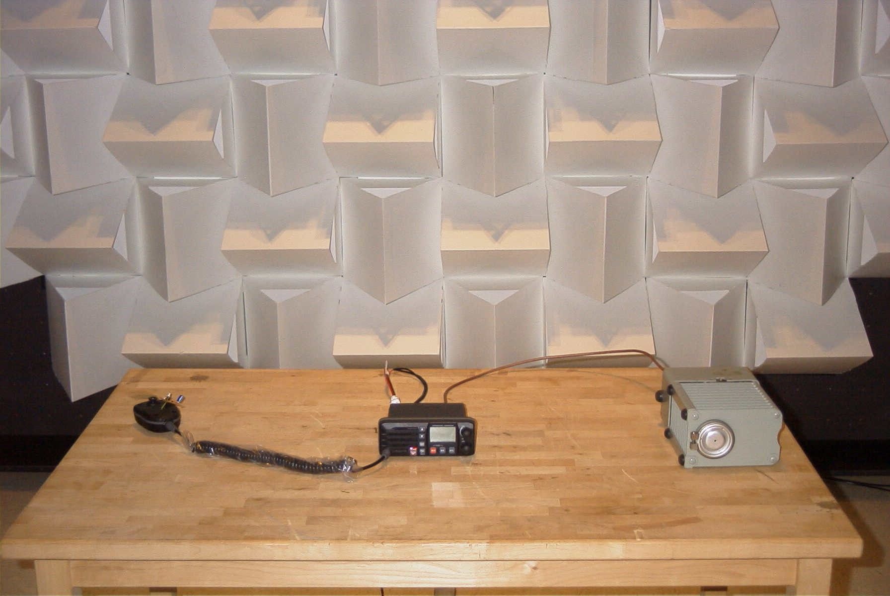
FCC ID: K6630303X3S IC ID: 511B-30303X3S Vertex Standard Co., Ltd. Front view Rear view FCC ID: K6630303X3S IC ID: 511B-30303X3S Vertex Standard Co., Ltd. Left side view Right side view FCC ID: K6630303X3S IC ID: 511B-30303X3S Vertex Standard Co., Ltd. Top view Bottom view FCC ID: K6630303X3S IC ID: 511B-30303X3S Vertex Standard Co., Ltd. Microphone DC Cable
ID Label/Location Info
GX1000S LABEL DRAWING Vertex Standard Co., Ltd. ID / Part 15.19 and CAUTION drawings ID drawing Part 15.19 and CAUTION drawings Label location This device complies with part 15 of the FCC Rules. Operation is subject to the condition that this device does not cause harmful interference. Device restricted to occupational use to satisfy FCC RF exposure compliance. See owners manual for specific operating requirement. ! ! CAUTION GX1000S VERTEX STANDARD CO., LTD. MADE IN JAPAN IC: 511B-30303X3S FCC ID: K6630303X3S 4909959000000 SER NO. 00000000
Internal Photos
FCC ID: K6630303X3S IC ID: 511B-30303X3S Vertex Standard Co., Ltd. Top of EUT without case Bottom of EUT without case FCC ID: K6630303X3S IC ID: 511B-30303X3S Vertex Standard Co., Ltd. Side-A of MAIN-UNIT with shield cases Side-A of MAIN-UNIT without shield cases FCC ID: K6630303X3S IC ID: 511B-30303X3S Vertex Standard Co., Ltd. Side-B of MAIN-UNIT Side-A of CNTL-UNIT with LCD FCC ID: K6630303X3S IC ID: 511B-30303X3S Vertex Standard Co., Ltd. Side-A of CNTL-UNIT without LCD Side-B of CNTL-UNIT FCC ID: K6630303X3S IC ID: 511B-30303X3S Vertex Standard Co., Ltd. Front of LCD Rear of LCD FCC ID: K6630303X3S IC ID: 511B-30303X3S Vertex Standard Co., Ltd. Side-A of VR-UNIT Side-B of VR-UNIT FCC ID: K6630303X3S IC ID: 511B-30303X3S Vertex Standard Co., Ltd. chassis Inside of panel FCC ID: K6630303X3S IC ID: 511B-30303X3S Vertex Standard Co., Ltd. Inside of microphone (1) Inside of microphone (2)
Operational Description
FCC ID:K6630303X3S IC ID: 511B-30303X3S Circuit Description 1 GX1000S Circuit Description Reception and transmission are switched the 8-bit MPU IC Q2004 (UPD78F0395) on the CNTL Unit. The receiver uses double-conversion superheterodyne circuitry, with a 21.4 MHz 1st IF and 450 kHz 2nd IF. The 1st local is produced by a PLL synthesizer, yielding the 21.4 MHz 1st IF. The 2nd local uses a 21.850 MHz crystal oscillator, yielding the 450 kHz 2nd IF. The 2nd mixer and other circuits use a custom IC to convert and amplify the 2nd IF and detect FM to obtain demodulated signals. During transmit, the PLL synthesizer oscillates at the desired frequency directly, for amplification to obtain RF power output. During transmit, voice modulation is applied to this synthesizer. Transceiver functions, such as TX/RX control, PLL synthesizer settings, and channel programming, are controlled using the MPU. RECEIVER Incoming RF signals from the antenna connector are delivered to the RF Unit, and pass through a low-pass filter (LPF) consisting of coils L1001 & L1002 and capacitors C1003,C1011,C1024&C1027, and antenna switching diode D1003・D1004 (L308CCB) for delivery to the receiver front end. Signals within the frequency range of the transceiver are then passed through a bandpass filter consisting of coils L1010 & L1012 and capacitors C1061, C1067, C1074, C1077, & C1083, before RF amplification by Q1022 (3SK294). The amplified RF is then passed through a bandpass filter again consisting of coils L1022, L1026, & L1027 and capacitors C1145, C1150, C1155, C1159, C1169, C1170, C1174&C1179, the pure in-band input signal is delivered to 1st mixer Q1028 (3SK131). Buffered output from the VCO is amplified by Q1017 (2SC5006) and low-pass filtered by coils L1009, L1011, & L1013 and capacitors C1060, C1064, C1071,C1076&C1079, to provide a pure 1st local signal between 134.65MHz and 141.875 MHz for delivery to the 1st mixer Q1028 (3SK131). The 21.4 MHz 1st mixer product then passes through monolithic crystal filters XF1001 (±6.5 kHz BW), and is amplified by Q1036 (2SC4400-3) and delivered to the input of the FM IF subsystem IC Q1029 (TA31136FN). This IC contains the 2nd mixer, 2nd local oscillator, limiter amplifier, FM detector, noise amplifier, and squelch gates. The 2nd local in the FM IF subsystem IC is produced from crystal X1001 (21.850 MHz), and the 1st IF is converted to 450 kHz by the 2nd mixer and stripped of unwanted components by ceramic filter CF1001. After passing through a limiter amplifier, the signal is demodulated by the FM detector. FCC ID:K6630303X3S IC ID: 511B-30303X3S Circuit Description 2 Demodulated receive audio from the FM IF subsystem IC is amplified by Q1033 and Q1038 (both 2SC4154E). The audio signal is passed through the AF Mute switch Q1031 (2SK2035) to the AF power amplifier Q1049 (LA4425A), the audio signal is delivered to the 16 Ohm internal loudspeaker and external Speaker terminal in the accessory cable. PLL SYNTHESIZER The 1st Local signal maintains stability from the PLL synthesizer by using a 21.850 MHz reference signal from crystal X1001. PLL synthesizer IC Q1026 (TB31202FNG) consists of a prescaler, reference counter, swallow counter, programmable counter, a serial data input port to set these counters based on the external data, a phase comparator, and a charge pump. The PLL synthesizer IC divides the 21.850 MHz reference signal by 1748 using the reference counter (12.5 kHz comparison frequency). The reference oscillator feeds to the PLL synthesizer IC Q1026 (TB31202FNG). for the 2nd local signal. The VCO output is divided by the prescaler, swallow counter and programmable counter. These two signals are compared by the phase comparator, and applied to the charge pump. A voltage proportional to their phase difference is delivered to the low-pass filter circuit, then fed back to the VCO as a voltage with phase error, controlling and stabilizing the oscillating frequency. This synthesizer also operates as a modulator during transmit. The VCO is consisted of Q1019 (2SK210GR) and varactor diodes D1009, D1011 (all HVU359), which oscillates at 21.4 MHz below from the receiving frequency. The VCO output passes through buffer amplifier Q1017,Q1018(2SC5006) to obtain stable output, then applied to the 1st mixer Q1031 (3SK131). The DC supply for the VCO is regulated by Q1016 (2SC4154E). TRANSMITTER Voice audio from the microphone is delivered via the MIC connector to the MAIN Unit. After passing through microphone amplifier Q1001 (LM2902PW), a pre-emphasis network, limiter (IDC: instantaneous deviation control), and low-pass filter network Q1001 (LM2902PW), the audio is adjusted for optimum deviation level and delivered to the next stage. Voice or DSC (Digital Selective Calling) encode signal inputs from the low-pass filter network Q1001 (LM2902PW) is by the VCO Q1019 (2SK210GR) and varactor diode D1009, D1011 (all HVU359), which oscillates the fundamental transmit frequency with direct frequency-modulation using varactor diode D1010(1SV214). The modulated signal passes through buffer amplifier Q1018 and Q1017 (both 2SC5006), diode switch D1006 FCC ID:K6630303X3S IC ID: 511B-30303X3S Circuit Description 3 (DAN235U) to drive amplifiers Q1008 (2SC5006) and RF power amplifier module Q1014 (S-AV37A). The RF energy then passes through antenna switch D1003 (L308CCB) and low-pass filter (LPF) consisting of coils L1001 & L1002 and capacitors C1003, C1011, C1024&C1027 and finally to the antenna connector. RF output power from the RF power amplifier module Q1014 (S-AV37A) is sampled by C1014 and C1021 and is rectified by D1002 (1SS321). The resulting DC is fed through Automatic Power Controllers Q1002 (LM2904PW) to RF power amplifier module Q1014 (S- AV37A), thus providing positive control of the power output. Generation of spurious products by the transmitter is minimized by the fundamental carrier frequency being equal to the final transmitting frequency, modulated directly in the transmit VCO. Add…
Text truncated - open the document above for the full version.
Parts List/Tune Up Info
FCC ID: K6630303X3S IC ID: 511B-30303X3S Alignment 1/6 Vertex Standard Co,. Ltd. GX1000S Alignment The GX1000S has been carefully aligned at the factory for the specified performance across the marine band. Realignment should therefore not be necessary except in the event of a component failure. All component replacement and service should be performed only by an authorized Standard Horizon representative, or the warranty policy may be voided. The following procedures cover the sometimes critical and tedious adjustments that are not normally required once the transceiver has left the factory. However, if damage occurs and some parts are replaced, realignment may be required. If a sudden problem occurs during normal operation, it is likely due to component failure; realignment should not be done until after the faulty component has been replaced. We recommend that servicing be performed only by authorized Standard Horizon service technicians who are experienced with the circuitry and fully equipped for repair and alignment. Therefore, if a fault is suspected, contact the dealer from whom the transceiver was purchased for instructions regarding repair. Authorized Standard Horizon service technicians realign all circuits and make complete performance checks to ensure compliance with factory specifications after replacing any faulty components. Those who do undertake any of the following alignments are cautioned to proceed at their own risk. Problems caused by unauthorized attempts at realignment are not covered by the warranty policy. Also, Standard Horizon, a division of VERTEX STANDARD, must reserve the right to change circuits and alignment procedures in the interest of improved performance, without notifying owners. Under no circumstances should any alignment be attempted unless the normal function and operation of the transceiver are clearly understood, the cause of the malfunction has been clearly pinpointed and any faulty components replaced, and the need for realignment determined to be absolutely necessary. The following test equipment (and thorough familiarity with its correct use) is necessary for complete realignment. Correction of problems caused by misalignment resulting from use of improper test equipment is not covered under the warranty policy. While most steps do not require all of the equipment listed, the interactions of some adjustments may require that more complex adjustments be performed afterwards. Do not attempt to perform only a single step unless it is clearly isolated electrically from all other steps. Have all test equipment ready before beginning, and follow all of the steps in a section in the order presented. FCC ID: K6630303X3S IC ID: 511B-30303X3S Alignment 2/6 Vertex Standard Co,. Ltd. Required Test Equipment RF Signal Generator with calibrated output level at 200 MHz Deviation Meter (linear detector) AF Millivoltmeter SINAD Meter Inline Wattmeter with 5% accuracy at 200 MHz Regulated DC Power Supply: 13.8 VDC, 10A 50-ohm Non-reactive Dummy Load: 30W at 200 MHz Frequency Counter: >0.1 ppm accuracy at 200 MHz AF Signal Generator DC Voltmeter: high impedance VHF Sampling Coupler AF Dummy Load: 4 Ohms, 10 W Oscilloscope Spectrum Analyzer Portable Marine Transceiver Alignment Preparation & Precautions A dummy load and inline wattmeter must be connected to the main antenna jack in all procedures that call for transmission. Correct alignment is not possible with an antenna. After completing one step, read the following step to determine whether the same test equipment will be required. If not, remove the test equipment (except dummy load and wattmeter, if connected) before proceeding. Correct alignment requires that the ambient temperature be the same as that of the transceiver and test equipment, and that this temperature be held constant between 20°C and 30°C (68°F and 86°F). When the transceiver is brought into the shop from hot or cold air it should be allowed some time for thermal equalization with the environment before alignment. If possible, alignments should be made with oscillator shields and circuit boards firmly affixed in place. Also, the test equipment must be thoroughly warmed up before beginning. Note: Signal levels in dB referred to in this procedure are based on 0 dBμ = 0.5 μV (closed circuit). Overview of Test Mode The test mode has been build in the microprocessor in order to adjust and confirm the performance of transceiver. The purpose is to adjust transceiver simply and to confirm the performance of transceiver smoothly. FCC ID: K6630303X3S IC ID: 511B-30303X3S Alignment 3/6 Vertex Standard Co,. Ltd. (A) In CH70, every time you are in transmit mode, (every time you press PTT), the following test tone can be outputted: 1st transmission: 1300 Hz 2nd transmission: 2100 Hz 3rd transmission: No modulation 4th transmission: Synthetic tone of 1300 Hz and 2100 Hz 5th transmission: Return to 1st transmission (B) Scan the channels between WX10 and EXP04 in the SCAN mode. Starting Test Mode Confirm that PWR/VOL switch is off, and short the TEST points(JP1001). Turn on the PWR/VOL switch while press and holding the DIST and W/X keys. Adjustment and Confirmation of Transmit Power Adjust power at high and low in the transmit mode, and confirm power in the specified bandwidth. -- Adjustment -- Connect the wattmeter and 50-ohm dummy load to the antenna jack. Use the H/L key to set transceiver to high power and set the channel to CH16. With the PTT switch pressed, adjust VR1001 so that RF power is 25 W. Use the H/L key to set transceiver to low power and set the channel to CH16. With the PTT switch pressed, adjust VR1002 so that RF power is 0.8 W. Adjustment of PLL Frequency Adjust the frequency in the transmit mode and local frequency in the receive mode. Setup the test equipment as shown below. Set the channel to CH16. With the PTT switch pressed, adjust TC1001 so that RF frequency is 156.80000 MHz ± 100 Hz. Adjus…
Text truncated - open the document above for the full version.
Parts List/Tune Up Info
1 FCC ID: K6630303X3S/IC ID: 511B-30303X3S GX1000SSemi-Conductor Parts List Address Parts Code Device NameDescriptionTYP VAL MAIN-UNIT D 1001 G2090800 Diode1N5402 D 1002 G2070076 Diode1SS321(TE85R.F) D 1003 G2090792 DiodeL308CCB D 1004 G2090792 DiodeL308CCB D 1005 G2070118 DiodeHSU277TRF D 1006 G2070176 DiodeDAN235U TL D 1007 G2070118 DiodeHSU277TRF D 1008 G2070118 DiodeHSU277TRF D 1009 G2070452 DiodeHVU359 TRF-E D 1010 G2070356 Diode1SV214(TPH2.F) D 1011 G2070452 DiodeHVU359 TRF-E D 1012 G2071212 DiodeBZT52-B5V6S D 1013 G2070704 DiodeMC2850-T111-1 D 1014 G2070704 DiodeMC2850-T111-1 Q 1001 G1094009 ICLM2902PWR Q 1002 G1094010 ICLM2904PWR Q 1003 G3070247 TransistorRT1N441U-T11-1 Q 1004 G3070074 TransistorDTA144EE TL Q 1005 G3070022 TransistorDTB123EK T146 Q 1006 G3070247 TransistorRT1N441U-T11-1 Q 1007 G3070247 TransistorRT1N441U-T11-1 Q 1008 G3350068 Transistor2SC5006-T1 Q 1009 G3070022 TransistorDTB123EK T146 Q 1010 G3070247 TransistorRT1N441U-T11-1 Q 1011 G3070247 TransistorRT1N441U-T11-1 Q 1012 G1093660 ICNJM78M05DL1A-TE1 Q 1013 G1093802 ICNJM7808DL1A-TE1 Q 1014 G1094559 PWR-MODULE S-AV37A(VX.F) Q 1015 G3070247 TransistorRT1N441U-T11-1 Q 1016 G3341548E Transistor2SC4154-T11-1E Q 1017 G3350068 Transistor2SC5006-T1 Q 1018 G3350068 Transistor2SC5006-T1 Q 1019 G3802107G FET2SK210GR(TE85R.F) Q 1021 G3070249 TransistorRT1N241M-T11-1 Q 1022 G4802948 FET3SK294(TE85L) Q 1023 G3341548E Transistor2SC4154-T11-1E Q 1024 G3341548E Transistor2SC4154-T11-1E Q 1026 G1094103 ICTB31202FNG(TAPE) Q 1027 G3070074 TransistorDTA144EE TL Q 1028 G4801317B FET3SK131-T2B V12 Q 1029 G1091605 ICTA31136FNG(EL) Q 1031 G3820357 FET2SK2035 TE85R Q 1032 G3070247 TransistorRT1N441U-T11-1 Q 1033 G3341548E Transistor2SC4154-T11-1E Q 1034 G1092943 ICNJM2211M-TE1 Q 1035 G3341548E Transistor2SC4154-T11-1E Q 1036 G3344008C Transistor2SC4400-3-TL Q 1037 G3341548E Transistor2SC4154-T11-1E Q 1038 G3341548E Transistor2SC4154-T11-1E Q 1039 G1092241 ICLA4425A Q 1040 G1090893 ICTC4S66F(TE85R.F) Q 1041 G3070247 TransistorRT1N441U-T11-1 Vertex Standard Co.,Ltd. 2 FCC ID: K6630303X3S/IC ID: 511B-30303X3S GX1000SSemi-Conductor Parts List Address Parts Code Device NameDescriptionTYP VAL CNTL-UNIT D 2001 G2071200 Diode1SS355(TAPE) D 2002 G2070078 DiodeIMN10 T108 D 2003 G2071104 LEDSML-512WWT86 D 2004 G2071104 LEDSML-512WWT86 D 2005 G2071104 LEDSML-512WWT86 D 2006 G2071104 LEDSML-512WWT86 D 2007 G2071104 LEDSML-512WWT86 D 2008 G2071104 LEDSML-512WWT86 DS2001 G6090184 LCDAM030N Q 2001 G3070247 TransistorRT1N441U-T11-1 Q 2002 G0090039 PhotocouplerPC3H7CDJ000F Q 2003 G1092589 ICPST597CNR Q 2004 G1094521 ICUPD78F0395GC-8EA-A Q 2006 G1094519 ICBR24L08FVT-W(TAPE) Q 2007 G3341548E Transistor2SC4154-T11-1E Q 2008 G3211327R Transistor2SB1132 T100 R Vertex Standard Co.,Ltd.
RF Exposure Info
9/17/2007 Page 1 of 3 FCC ID: K6630303X3S FCC RF Exposure Requirements General information : FCC ID: K6630303X3S Device category: Mobile per Part 2.1091 Environment: Uncontrolled Exposure Mobile devices that operate under Part 80 of this chapter are subject to routine environmental evaluation for RF exposure prior to equipment authorization or use if they operate at frequencies of 1.5 GHz or below and their effective radiated power (ERP) is 1.5 watts or more. However, compliance with the power density limits of 1.1310 is not required. Antenna: The manufacturer does specify an antenna with a gain of 3 dBi to be used with this device. This device has provisions for operation in a vehicle (marine vessel), or a fixed location. Configuration Antenna p/n Type Max. Gain (dBi) Boat Any omni 3 Operating configuration and exposure conditions: The conducted output power is 25 Watts. Typical use qualifies for a maximum duty cycle factor of 50%. - Part 2.1091 states that devices are excluded from routine evaluation if the EIRP is less than 2.46Watt (or 1.5WERP). - Vehicle Operation: The maximum antenna gain that can be used is 3dBi. A coaxial cable of the type RG 58 has a loss of 1dB for a length of 15 feet. MPE Calculation: The minimum separation distance is calculated as follows: The limit for uncontrolled exposure environment below 300 MHz is 0.2 mW/cm 2 . 9/17/2007 Page 2 of 3 FCC ID: K6630303X3S Channel frequency: 156.025-157.425 MHz The conducted power output is 25 watt. The coax loss was taken as 1 dB. Antenna gain was taken as 3 dBi 50% talk time in 30 minutes For all VHF frequencies dBd0.85:=CL1:=dB S is fixed at 0.2 mw/cm^2 GdBd2.15+CL−:= f300:= G2= Net gain in dBi S f 1500 := Gn10 G 10 := S0.2= mW cm 2 from OET 65 Gn1.585= Gain Numeric R W1exp Gn⋅() 4π⋅S⋅ () := Rinches R 2.54 := R88.784= distance in centimeters Rinches34.954= required for compliance Power in WattsDuty Factor in decimal % (1=100%) W25:=D1:= for an FM device D=1 Exposure time in minutes U30:= (use 6 for controlled and 30 for uncontrolled) E15:= PC E U := percent on time WexpW D⋅ E U ⎛ ⎜ ⎝ ⎞ ⎟ ⎠ ⋅:= PC0.5= Time compensated power output Wexp12.5=Watts W1expWexp 1000⋅:= W1exp1.2510 4 ×=mWatts ___________________________________________________________________________ Antenna gainCoax Loss 9/17/2007 Page 3 of 3 FCC ID: K6630303X3S Conclusion: The device complies with the MPE requirements by providing a safe separation distance of 0.89m between an antenna with a gain of 3 dBi, including any radiating structure, and any persons when normally operated . Proposed RF exposure safety information to include in User’s Manual : “FCC RF Exposure Requirements: CAUTION: The antenna(s) used for this transmitter must not be co-located or operating in conjunction with any other antenna or transmitter. This device is approved with emissions having a source-based time-averaging duty factor not exceeding 50%. These figures are based on a antenna having a 3 dBi gain. Failure to observe these restrictions will result in exceeding the FCC RF exposure limits.
Test Report
Page 1 of 35 REPORT ON Radio testing of the STANDARD HORIZON GX1000S In accordance with ANSI/TIA/EIA-603, RSS-182 August 2007Report number TA000552 Vertex Standard Co., Ltd. GENERAL INFORMATION TRANSMITTERS x Switchable Variable N/ A RECEIVERS This re port was prepared by Vertex Standard Co., Ltd. MODEL NAME: Report number TA000552Page 2 of 35 NUMBER OF CHANNELS: FCC ID: TRADE NAME: VHF FM Mobile TransceiverEUT DESCRIPTION: 13.8 7J000001 MANUFACTURER:Vertex Standard Co., Ltd. IC ID: TYPE OF EMISSION: FREQUENCY RANGE: RSS-182 VOLTAGE RQUIREMENTS: SERIAL NUMBER: SPECIFICATION ARE REFERENCE D POWER OUTPUT RATING: 156.1 1 157.4to to25 [MHz] [W] 16K0G3E, 16K0G2B( for DSC) [MHz] [W] [Ω] [Ω] [Ω] [Ω] [MHz] [kHz] -21.4 -450 [W]AUDIO OUTPUT POWER: OUTPUT IMPEDANCE (SP):[Ω]4 4.5 [V] GX1000S K6630303X3S STANDARD HORIZON 511B-30303X3S INPUT IMPEDANCE (MIC): MAXIMUM POWER RATING: INPUT IMPEDANCE (RF): INTERMEDIATE FREQUENCIES: FREQUENCY RANGE: OUTPUT IMPEDANCE (RF): OUTPUT IMPEDANCE (RF): Collector Current: Date 09 / August /2007 Test performed by M.Kurihara 156.050 to163.475 50 1st 2nd 50 2000 25 DC 65 ANSI/TIA/EIA-603 50 4.5[A] Collector Voltage:13.8[V] Vertex Standard Co., Ltd. GX1000S Channel Settings HILOW 1CH16156.800156.80025k25W1W 2CH70156.525156.52525k25W1W 3 4 5 6 7 8 9 10 11 12 13 14 15 16 17 18 19 20 Report number TA000552Page 3 of 35 Power Transmit Frequency [MHz] CH No. Receive Frequency [MHz] CH Spacing Shown on LCD Vertex Standard Co., Ltd. NAME OF TEST:R.F. Power Output (Conducted) SPECIFICATION:47 CFR 2.1046 (a) GUIDE:ANSI/TIA/EIA-603, Paragraph 2.2.1 TEST EQUIPMENT: As per attached page The EUT was connected to a resistive coaxial attenuator of normal load impedance, and the modulated output powerwas measured by means of an R.F. power meter. Measurement accuracy is ± 4% MEASUREMENT PROCEDURE 22.900 NOMINAL, MHz 70 0.840 0.840 1. 2. MEASUREMENT RESULTS 156.800 CHANNEL R.F. POWER, WATTS 16 HIGH Report number TA000552Page 4 of 35 23.800 156.525 LOW Vertex Standard Co., Ltd. (1) COAXUAL ATTENUATORWEINSCHELL 49-10-43KL458 (2) RF COUPLERADVANTEST TR415339730008 2349A02533 (2) Agilent 8901B POWER MODE3026A02806 (4) POWER METER (3) POWER SENSORAgilent 8482B Serial NumberInstruments Test Sample (5) FREQUENCY COUNTERAgilent 8901B FREQUENCY MODE3026A02806 TRANSMITTER POWER CONDUCTED MEASUREMENTS Power Supply TEST 1: R.F. POWER OUTPUT TEST 2: FREQUENCY STABILIT Y (4)(3)(1) Description (5) Report number TA000552Page 5 of 35 Vertex Standard Co., Ltd. NAME OF…
Text truncated - open the document above for the full version.
Contact Information
Applicant
Masatoshi Muraishi(Engineering Division)
Test Firm
Timco Engineering, Inc.Sid Sanders
Technical Specifications
| # | Rule Parts | Frequency Range | Power Output | Emission | Tolerance |
|---|---|---|---|---|---|
| 4 | 8 | 156.025 MHz - 157.425 MHz | 1 W | 16K0G2B | 10 ppm |
Other Applications from Yaesu Musen Co., Ltd.
K660E180X10
Dec 01, 2025BLUETOOTH MICROPHONE
Equipment Class
DTS - Digital Transmission System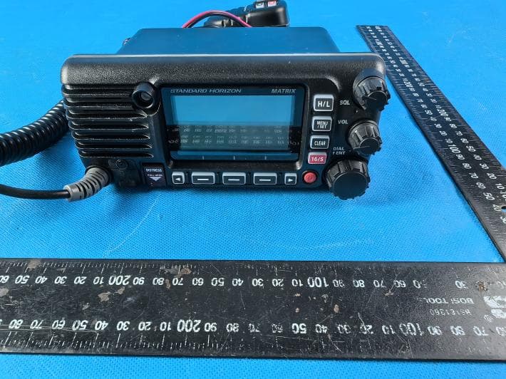
K6630673Y3D
Aug 01, 2024VHF FM Marine Transceiver
Equipment Class
CXX - Communications Rcvr for use w/ licensed Tx and CBs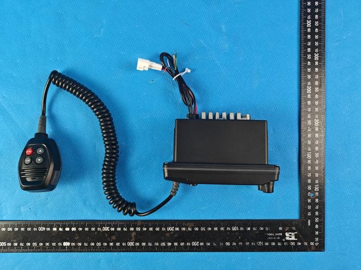
K6630653Y3D
Aug 01, 2024VHF FM Marine Transceiver
Equipment Class
CXX - Communications Rcvr for use w/ licensed Tx and CBs
K6630683X30
Jan 10, 2023VHF FM Marine Transceiver
Equipment Class
TNF - Licensed Non-Broadcast Transmitter Held to Face
K6650033X30
Nov 18, 2020Airband Radio Transceiver
Equipment Class
TNF - Licensed Non-Broadcast Transmitter Held to Face