K6630313X30HANDHELD VHF TRANSCEIVER
Yaesu Musen Co., Ltd.
Click to zoom
Application Details
- Equipment Class
- TNF - Licensed Non-Broadcast Transmitter Held to Face
- Date of Grant
- Feb 03, 2008
- Application Purpose
- Original Equipment
- Date of Application
- Feb 03, 2008
- Equipment Note
- HANDHELD VHF TRANSCEIVER
- Frequency Range
- 156.02500000 - 157.42500000
- Company
- Yaesu Musen Co., Ltd.
- Country
- Japan
Documents & Files
Document Text
Text extracted from the exhibit documents filed with the FCC. Open a document above to read the original.
Users Manual
FCC ID:K6630313X30 IC ID:511B-30313X30 Operating Manual Vertex Standard Co.,Ltd. 1 Operating Manual Congratulations on your purchase of the HX850S! Whether this is your first portable marine VHF transceiver, or if you have other STANDARD HORIZON equipment, the STANDARD HORIZON organization is committed to ensuring your enjoyment of this high performance transceiver, which should provide you with many years of satisfying communications even in the harshest of environments. STANDARD HORIZON technical support personnel stands behind every product sold, and we invite you to contact us should you require technical advice or assistance. We appreciate your purchase of the HX850S, and encourage you to read this manual thoroughly, so as to learn and fully understand the capabilities of the HX850S. WARNING This radio is capable of transmitting on VHF Marine. The FCC allows the use of VHF Marine band on water areas only. However the FCC does not allow the use of the VHF Marine band when on land. If persons use the VHF Marine Band on land and interfere with others communicating, the FCC will be notified and search for the interference. Responsible parties found to be transmitting on the VHF Marine Band on land could be fined up to $10,000 for the first offense. The FCC does however prohibit the use in aircraft. RF EXPOSURE SAFETY STATEMENT SAFETY INFORMATION Your wireless handheld portable transceiver contains a low power transmitter. When the Push-to-Talk (PTT) button is pushed, the transceiver sends out radio frequency (RF) signals. In August 1996, the Federal Communications Commission adopted RF exposure guidelines with safety levels for hand-held wireless devices. This device is authorized to operate at a duty factor not to exceed 50% (this corresponds to 50% transmission time and 50% reception time). WARNING: To maintain compliance with the FCC’s RF exposure guidelines, this transmitter and its antenna must maintain a separation distance of at least 1 inch (2.5 centimeters) from your face. Speak in a normal voice, with the antenna pointed up and away from the face at the required separation distance. If you use a headset accessory for this radio, with the radio worn on your body, use only the Vertex Standard belt clip for this transceiver, and ensure that the antenna is at least 1 inch (2.5 centimeters) from your body when transmitting. Use only the supplied antenna. Unauthorized antennas, modifications, or attachments could damage the transmitter, and may violate FCC regulations. NOTE This radio telephone complies with the requirements of RTCM Paper 56-95/SC101 Standards for digital selective calling (DSC) for Marine transceivers. FCC AND CANADA RADIO LICENSE INFORMATION Standard Horizon radios comply with the Federal Communication Commission (FCC) and FCC ID:K6630313X30 IC ID:511B-30313X30 Operating Manual Vertex Standard Co.,Ltd. 2 Industry-Canada requirements that regulate the Maritime Radio Service. MARITIME STATION LICENSE An FCC ship station license is no longer required for any vessel traveling in U.S. waters which uses a VHF marine radio, RADAR or EPIRB, and which is not required to carry radio equipment. However, any vessel required to carry a marine radio on an international voyage, carrying a HF single side band radiotelephone or marine satellite terminal. FCC license forms, including applications for ship (506) and land station licenses can be downloaded via the Internet at www.fcc.gov/forms. To obtain a form from the FCC, call (888) 225-5322. MARINE RADIO CALL SIGN Currently the FCC does not require recreational boaters to have a Ship Radio Station License. The USCG recommends the boats registration number and the state to be used. CANADIAN SHIP STATION LICENSING You may need a license when traveling in Canada. If you do need a license contact their nearest field office or regional office or write: Industry Canada Radio Regulatory Branch Attn: DOSP 300 Slater Street Ottawa, Ontario Canada, KIA 0C8 FCC/INDUSTRY CANADA INFORMATON The following data pertaining to the transceiver is necessary to fill out the license application. FCC Type Accepted: Part 80 Output Power with FNB-V99LI: 1 W (Low), 2.5 W (Mid) ,5 W (High) , and 6 W (Nor) Emission: 16K0G3E, 16K0G2B Frequency Range: 156.025 to 163.275MHz FCC Type Number: Industry Canada Type Approval: FCC NOTICE FCC ID:K6630313X30 IC ID:511B-30313X30 Operating Manual Vertex Standard Co.,Ltd. 3 Unauthorized changes or modifications to this equipment may void compliance with FCC Rules. Any change or modification must be approved in writing by STANDARD HORIZON, a Marine Division of VERTEX STANDARD. NOTICE This equipment has been tested and found to comply with the limits for a Class B digital device, pursuant to Part 15 of the FCC Rules. These limits are designed to provide reasonable protection against harmful interference in a residential installation. This equipment generates uses and can radiate radio frequency energy and, if not installed and used in accordance with the instructions, may cause harmful interference to radio communications. However, there is no guarantee that interference will not occur in a particular installation. If this equipment does cause harmful interference to radio or television reception, which can be determined by turning the equipment off and on, the user is encouraged to try to correct the interference by one or more of the following measures: Increase the separation between the equipment and receiver. Connect the equipment into an outlet on a circuit different from that to which the receiver is connected. Consult the dealer or an experienced marine electronics technician for help. 1. GENERAL INFORMATION 1.1 INTRODUCTION The HX850S is a SUBMERSIBLE miniature 6-Watt portable two way marine transceiver. The transceiver has all allocated USA, International, or Canadian channels. It has emergency channel 16 which can be immediately selected from any channel by pressing the [16/9] key. NOAA Weather channels ca…
Text truncated - open the document above for the full version.
Cover Letter(s)
December 17, 2007 Federal Communications Commission Authorization and Evaluation Division, 7435 Oakland Mills Road Columbia, MD 21046 USA Re: HX850S (FCC ID: K6630313X30) Gentlemen: Part 15.19 Compliance Statement is placed on the rear of case. Sincerely, Vertex Standard Co., Ltd. Yukimasa Tomita Director of Engineering Division
Cover Letter(s)
December 17, 2007 Federal Communications Commission Authorization and Evaluation Division, 7435 Oakland Mills Road Columbia, MD 21046 USA Re: HX850S (FCC ID: K6630313X30) Gentlemen: A. Part 15.21 Compliance Statement Drawing: B. Part 15.21 Compliance Statement Drawing Location: IN OPERATION MANUAL (location on the back cover page) Sincerely, Vertex Standard Co., Ltd. Yukimasa Tomita Director of Engineering Division Part 15.21: Changes or modifications to this device not expressly approved by Vertex Standard could void the user’s authorization to operate this device. 20mm 97mm
Cover Letter(s)
December 17, 2007 Federal Communications Commission EQUIPMENT APPROVAL SERVICES P. O. Box 358315 Pittsburgh, PA 15251-5315 Attention: Authorization and Evaluation Division Reference: HX850S (FCC ID: K6630313X30) Pursuant to Sections 0.457 (d)(1)(ii) and 0.459 of the Commission’s Rules, the Applicant hereby requires confidential treatment of some of the information accompanying this Application, as listed below: ・ Block Diagram ・ Schematics These materials contain trade secrets and proprietary information not customarily released to the public. The public disclosure of these matters might be harmful to the Applicant and provide unjustified benefits to its competitors. The Applicant understands that pursuant to Rule 0.457 (d)(1)(ii), disclosure of the Application and all accompanying documentation will not be made before the date of Grant for this Application. Sincerely, Vertex Standard Co., Ltd Yukimasa Tomita Director of Engineering Division
External Photos
FCC ID:K6630313X30 IC ID:511B-30313X30 Vertex Standard Co., Ltd. Front view with Antenna Rear view with Antenna FCC ID:K6630313X30 IC ID:511B-30313X30 Vertex Standard Co., Ltd. Front view without Antenna Rear view without Antenna FCC ID:K6630313X30 IC ID:511B-30313X30 Vertex Standard Co., Ltd. Right view Left view FCC ID:K6630313X30 IC ID:511B-30313X30 Vertex Standard Co., Ltd. Top view Bottom view FCC ID:K6630313X30 IC ID:511B-30313X30 Vertex Standard Co., Ltd. Battery Pack (FNB-V99Li) Battery Pack (FNB-V99Li) FCC ID:K6630313X30 IC ID:511B-30313X30 Vertex Standard Co., Ltd. Alkaline Battery Case (FBA-38) Alkaline Battery Case (FBA-38) FCC ID:K6630313X30 IC ID:511B-30313X30 Vertex Standard Co., Ltd. Top of Battery Charger (CD-38) Side of Battery Charger (CD-38) FCC ID:K6630313X30 IC ID:511B-30313X30 Vertex Standard Co., Ltd. Top of AC Adapter (NC-88B) Bottom of AC Adapter FCC ID:K6630313X30 IC ID:511B-30313X30 Vertex Standard Co., Ltd. Antenna Belt Clip FCC ID:K6630313X30 IC ID:511B-30313X30 Vertex Standard Co., Ltd. Speaker/Microphone (MH-73A4B) Speaker/Microphone (CMP460) FCC ID:K6630313X30 IC ID:511B-30313X30 Vertex Standard Co., Ltd. Speaker/Microphone (MH-57A4B) VOX Headset (VC-24) FCC ID:K6630313X30 IC ID:511B-30313X30 Vertex Standard Co., Ltd. Earpiece Microphone (VC-27)
ID Label/Location Info
HX850SHX850S LABEL DRAWINGLABEL DRAWING Vertex Standard Co., Ltd.Vertex Standard Co., Ltd. ID / Part 15.19 and CAUTION drawings ID drawing Part 15.19 and CAUTION drawings Label location HX850S K6630313X30 511B-30313X30 4909959000000 ! ! Device restricted to occupational use to satisfy FCC RF exposure compliance. See owner's manual for specific operating requirement CAUTION This device complies with part 15 of the FCC Rules. Operation is subject to the condition that this device does not cause harmful interference.
Internal Photos
FCC ID:K6630313X30 IC ID: 511B-30313X30 Vertex Standard Co., Ltd. Removed Rear Panel with GPS Module Removed Rear Panel without GPS Module FCC ID:K6630313X30 IC ID: 511B-30313X30 Vertex Standard Co., Ltd. Side-A of MAIN-UNIT with LCD Side-A of MAIN-UNIT without LCD FCC ID:K6630313X30 IC ID: 511B-30313X30 Vertex Standard Co., Ltd. Side-B of MAIN-UNIT Without chassis Side-B of MAIN-UNIT With chassis FCC ID:K6630313X30 IC ID: 511B-30313X30 Vertex Standard Co., Ltd. GPS Module LCD (Front) FCC ID:K6630313X30 IC ID: 511B-30313X30 Vertex Standard Co., Ltd. LCD (Back) Inside of front panel FCC ID:K6630313X30 IC ID: 511B-30313X30 Vertex Standard Co., Ltd. Inside of Rear panel Inside of chassis (Front) FCC ID:K6630313X30 IC ID: 511B-30313X30 Vertex Standard Co., Ltd. Inside of chassis (Back) Inside of MH-73A4B (side A) FCC ID:K6630313X30 IC ID: 511B-30313X30 Vertex Standard Co., Ltd. Inside of MH-73A4B (side B)
Operational Description
FCC ID: K6630313X30 IC ID: 511B-30313X30 Circuit Description Vertex Standard Co., Ltd. 1 Circuit Description Receiver RF signals pass through a low-pass filter, an antenna switching circuit consisting of D1004 (RLS135) and D1005 (RLS135) and a high-pass filter. Passed signals are amplified with a FET transistor Q1018 (3SK294). Amplified signals are filtered by a band-pass filter to remove unwanted signals. Filtered signals are delivered to the first mixer to generate the first intermediate frequency (IF). A local signal made by a VCO is input into the first mixer Q1025 (3SK318), then it generates the 1 st IF at 47.25MHz. The 1 st IF passes through a monolithic crystal filter XF1001 (47.25MHz) to the IF amplifier Q1028 (2SC4915-0). And the 1 st IF is input into the FM IC Q1031 (NJM2591V). The 2 nd local signal (46.8MHz) which is multiplied a crystal oscillator 11.7MHz fourfold with a transistor Q1029 (2SC4915-0) is input into the FM IC. Inside of the FM IC, the 2 nd IF (450kHz) is generated by a mixer mixed with the 1 st IF and 2 nd local signal, then the 2 nd IF is filtered by a ceramic filter CF1001 (LTWC450F) and amplified by a limiting amplifier before quadrate detection by a ceramic discriminator CD1001 (JTBM450CX24) to demodulate. The demodulated audio signal passes through a de-emphasis network, a high-pass filter Q1046 (2SC4617-R) and a low-pass filter Q1041 (2SC4617-R) to a volume control IC Q1030 (BU2502FS). Controlled audio signal pass through a audio mute IC Q1034 (CD4066BPW) to the audio power amplifier Q1047 (TDA2822D) to provide up to 0.7 W to 16 Ohms loudspeaker. Squelch control Some part of the demodulated audio signal is input into an active band-pass filter inside of the FM IC. The output signal from this filter (which means the noise component) is rectified by D1026 and D1027 (both DA221) after amplified by a transistor Q1033 (2SC4617-R). As a result, obtained DC voltage is read by a CPU Q1032 (μPD78F1167GC). A CPU compares own squelch set point with this rectified DC. If the DC level is lower than the squelch set point, a CPU controls the mute circuit to mute the audio output. Modulation Voice signal from either a built-in microphone MC1001 (CZ034DP363) or an external jack J1001 is pre-emphasized by a pre-emphasis network C1231 and R1184. Pre-emphasized signal is amplified by an op-amp Q1003 (LM2904PW). Amplified signal passes through the IDC (instantaneous FCC ID: K6630313X30 IC ID: 511B-30313X30 Circuit Description Vertex Standard Co., Ltd. 2 deviation control) circuit and a low-pass filter networks Q1003 to a volume control IC Q1030. A volume control IC adjusts the modulation to optimum level. The voice signal is delivered to a varactor diode D1011 (HVC306B) in a VCO, then a VCO is modulated directly. Transmitter The modulated RF signal from a VCO pass through a diode switch D1023 (DAN235E) to a pre-amplifier Q1020 (2SC5226-5). Amplified RF signal is amplified by a driver-amplifier Q1015 (RD01MUS1) and amplified by a power-amplifier Q1009 (RD09MUP2) up to 6 W. The RF power output passes through antenna switching diode D1004 to a low-pass filter network. A low-pass filter suppresses harmonic spurious products before an antenna jack. Automatic Power Control Some part of the RF power is sampled by capacitors C1009 and C1020 and rectified by a diode D1003 (RB715F) to obtain the DC voltage level. This DC voltage is compared with the power control voltage from D/A IC Q1030 by op-amps Q1004 (LM2094PW). As a result, compared output voltage controls RF power devices’ bias to get the stable output. PLL Synthesizer The 1st Local signal maintains stability from the PLL synthesizer by using the 11.7 MHz reference signal from crystal X1001. PLL synthesizer IC Q1026 (LV2105V) consists of a prescaler, reference counter, swallow counter, programmable counter, a serial data input port to set these counters based on the external data, a phase comparator, and applied to the external charge pump which consists of Q1021 (2SA1774-R) and Q1038 (2SC4617-R). The PLL synthesizer IC divides the 11.7 MHz reference signal by 936 using the reference counter (12.5 kHz comparison frequency). The VCO output is divided by the prescaler, swallow counter and programmable counter. These two signals are compared by the phase comparator, and applied to the charge pump. A voltage proportional to their phase difference is delivered to the low-pass filter circuit, and then fed back to the VCO as a voltage with phase error, controlling and stabilizing the oscillating frequency. This synthesizer also operates as a modulator during transmit. The VCO consists of Q1010 (2SC5231CB) and varactor diodes D1008/1009 (all HVC350B), which oscillates at 47.25 MHz below from the receving frequency. And the VCO oscillates at the fundamental transmit frequency during a transmitting with direct frequency-modulation using FCC ID: K6630313X30 IC ID: 511B-30313X30 Circuit Description Vertex Standard Co., Ltd. 3 varactor diode D1011 (HVC306B). The VCO output is input into buffer amplifier Q1008 (2SC5006) to obtain stable output. The DC supply for the VCO is regulated by Q1017 (2SC4617-R). DSC Encoder/ Decoder Encoder CPU Q1032 encodes the DSC (Digital Selective Calling) signals. This signal is input into the op-amp Q1003. The processes of DSC transmitting are the same as voice modulation. Decoder The received DSC signals on channel 70 are filtered by a low-pass filter Q1037 (2SC4617-R). Then this signal is input into the FSK decoder IC Q1045 (NJM2211M) to convert the analog signal into the digital code. CPU Q1032 watches the digital code and is computing the DSC. 1050 Hz Weather Alert Decoder Some part of the signal from a low-pass filter output for the DSC is amplified by a transistor Q1038 (2SC4617-R). Amplified signal is input into the Schmitt inverter IC Q1006 (SN74LVC3G14DCT) to obtain the weather alert tone pulse. CPU Q1032 watches this pulse to count the weather alert tone frequency. MPU Operation is controlled by a CPU …
Text truncated - open the document above for the full version.
Parts List/Tune Up Info
FCC ID: K6630313X3D0 IC ID: 511B-30313X3D0 Alignment 1/6 Vertex Standard Co., Ltd. HX850S Alignment The HX850S has been carefully aligned at the factory for the specified performance across the marine band. Realignment should therefore not be necessary except in the event of a component failure. All component replacement and service should be performed only by an authorized Standard Horizon representative, or the warranty policy may be voided. The following procedures cover the sometimes critical and tedious adjustments that are not normally required once the transceiver has left the factory. However, if damage occurs and some parts are replaced, realignment may be required. If a sudden problem occurs during normal operation, it is likely due to component failure; realignment should not be done until after the faulty component has been replaced. We recommend that servicing be performed only by authorized Standard Horizon service technicians who are experienced with the circuitry and fully equipped for repair and alignment. Therefore, if a fault is suspected, contact the dealer from whom the transceiver was purchased for instructions regarding repair. Authorized Standard Horizon service technicians realign all circuits and make complete performance checks to ensure compliance with factory specifications after replacing any faulty components. Those who do undertake any of the following alignments are cautioned to proceed at their own risk. Problems caused by unauthorized attempts at realignment are not covered by the warranty policy. Also, Standard Horizon, a division of VERTEX STANDARD, must reserve the right to change circuits and alignment procedures in the interest of improved performance, without notifying owners. Under no circumstances should any alignment be attempted unless the normal function and operation of the transceiver are clearly understood, the cause of the malfunction has been clearly pinpointed and any faulty components replaced, and the need for realignment determined to be absolutely necessary. The following test equipment (and thorough familiarity with its correct use) is necessary for complete realignment. Correction of problems caused by misalignment resulting from use of improper test equipment is not covered under the warranty policy. While most steps do not require all of the equipment listed, the interactions of some adjustments may require that more complex adjustments be performed afterwards. Do not attempt to perform only a single step unless it is clearly isolated electrically from all other steps. Have all test equipment ready before beginning, and follow all of the steps in a section in the order presented. FCC ID: K6630313X3D0 IC ID: 511B-30313X3D0 Alignment 2/6 Vertex Standard Co., Ltd. Required Test Equipment RF Signal Generator with calibrated output level at 200 MHz Deviation Meter (linear detector) AF Millivoltmeter SINAD Meter Inline Wattmeter with 5% accuracy at 200 MHz Regulated DC Power Supply: 3 to 15 VDC, 2A 50-ohm Non-reactive Dummy Load: 10W at 200 MHz Frequency Counter: >0.1 ppm accuracy at 200 MHz AF Signal Generator DC Voltmeter: high impedance VHF Sampling Coupler AF Dummy Load: 8 Ohms, 3 W Oscilloscope Spectrum Analyzer Alignment Preparation & Precautions A dummy load and inline wattmeter must be connected to the main antenna jack in all procedures that call for transmission. Correct alignment is not possible with an antenna. After completing one step, read the following step to determine whether the same test equipment will be required. If not, remove the test equipment (except dummy load and wattmeter, if connected) before proceeding. Correct alignment requires that the ambient temperature be the same as that of the transceiver and test equipment, and that this temperature be held constant between 20°C and 30°C (68°F and 86°F). When the transceiver is brought into the shop from hot or cold air it should be allowed some time for thermal equalization with the environment before alignment. If possible, alignments should be made with oscillator shields and circuit boards firmly affixed in place. Also, the test equipment must be thoroughly warmed up before beginning. Note: Signal levels in dB referred to in this procedure are based on 0 dBμ = 0.5 μV (closed circuit). FCC ID: K6630313X3D0 IC ID: 511B-30313X3D0 Alignment 3/6 Vertex Standard Co., Ltd. Overview of the Test Mode The test mode has been build in the microprocessor in order to confirm the performance of transceiver. The purpose is to adjust transceiver simply and to confirm the performance of transceiver smoothly. (A) Expansion channels “EXP01 - EXP06” will be set as follows: DISPLAY RX Frequency TX Frequency EXP01 156.050 MHz 156.050 MHz EXP02 --- 157.425 MHz EXP03 163.275 MHz --- EXP04 155.050 MHz 155.050 MHz EXP05 162.025 MHz 162.025 MHz EXP06 163.575 MHz 158.975 MHz (B) In CH70, every time you are in transmit mode, (every time you press PTT), the following test tone can be outputted: 1st transmission: Synthetic tone of 1300 Hz and 2100 Hz 2nd transmission: 1300 Hz 3rd transmission: 2100 Hz 4th transmission: No modulation 5th transmission: Return to 1st transmission (C) Scan the channels between WX10 and EXP04 in the SCAN mode. (D) In the test mode, a transmit time-out timer function (TOT) becomes off. (E) A user’s MMSI is set to “0123456789” for DSC tests tempor Starting the Test Mode Press the [PWR] switch while pressing and holding the [DISTRESS] and [WX] keys to turn on. Confirmation of VCO Connect the DC voltmeter to the test point (LOCK TP). Set the channel to EXP06, confirm that the voltage on the TP1013 is more than 0.25V during receiving. Set the channel to EXP04, confirm that the voltage on the TP1013 is less than 3.8V during transmitting. FCC ID: K6630313X3D0 IC ID: 511B-30313X3D0 Alignment 4/6 Vertex Standard Co., Ltd. Overview of the Alignment Mode The alignment mode has been built in the microprocessor in order to adjust the perfor…
Text truncated - open the document above for the full version.
Parts List/Tune Up Info
1 FCC ID: K6630313X30/IC ID: 511B-30313X30 HX850SSemi-Conductor Parts List Address Parts Code Device NameDescriptionTYP VAL MAIN-UNIT D 1001 Q9000867 Surge Absorber EZAEG3A50AV D 1002 G2070634 Diode1SS400 TE61 D 1003 G2070752 DiodeRB715F T106 D 1004 G2070128 DiodeRLS135 TE-11 D 1005 G2070128 DiodeRLS135 TE-11 D 1006 G2070634 Diode1SS400 TE61 D 1007 G2070634 Diode1SS400 TE61 D 1008 G2070596 DiodeHVC350B-TRF-E D 1009 G2070596 DiodeHVC350B-TRF-E D 1011 G2070918 DiodeHVC306B TRU-E D 1012 G2071116 LEDSML-512DWT86 D 1013 G2071116 LEDSML-512DWT86 D 1014 G2071116 LEDSML-512DWT86 D 1015 G2071116 LEDSML-512DWT86 D 1016 G2071116 LEDSML-512DWT86 D 1017 G2071116 LEDSML-512DWT86 D 1018 G2071116 LEDSML-512DWT86 D 1019 G2071116 LEDSML-512DWT86 D 1020 G2071174 LEDWH104S(TAPE) D 1021 G2070860 LEDCL-165HR/YG-D-T D 1022 G2070848 Diode1SV325(TPH3.F) D 1023 G2070612 DiodeDAN235E TL D 1024 G2070178 DiodeDA221 TL D 1025 G2070078 DiodeIMN10 T108 D 1026 G2070178 DiodeDA221 TL D 1027 G2070178 DiodeDA221 TL D 1028 G2070634 Diode1SS400 TE61 D 1029 G2071222 Zener DiodeVMZ6.8NT2L D 1030 G2070538 Zener DiodeRD5.1UMB1-T1 D 1031 G2070642 DiodeRB521S-30 TE6 DS1001 G6090187 BTG-13264F-FBWB-N-G-A00RB521S-30 TE6 Q 1001 G1094549 ICTAR5S33U(TE85L.F) Q 1002 G1094097 ICTAR5S50U(TE85L.F) Q 1003 G1094009 ICLM2902PWR Q 1004 G1094010 ICLM2904PWR Q 1005 G1094097 ICTAR5S50U(TE85L.F) Q 1006 G1094258 ICSN74LVC3G14DCTR Q 1007 G1094056 ICS-812C33AUA-C2N-T2G Q 1008 G3350068 Transistor2SC5006-T1 Q 1009 G3070367 MOSFETRD09MUP2(TAPE) Q 1010 G3352318H Transistor2SC5231C8-TL Q 1011 G3070343 TransistorUMD5N TR Q 1012 G3070343 TransistorUMD5N TR Q 1013 G3070343 TransistorUMD5N TR Q 1014 G3070247 TransistorRT1N441U-T11-1 Q 1015 G3070321 MOSFETRD01MUS1-T113 Q 1016 G3070247 TransistorRT1N441U-T11-1 Q 1017 G3346178R Transistor2SC4617 TL R Q 1018 G4802948 FET3SK294(TE85L) Q 1019 G3070334 TransistorFMMTL618TA Q 1020 G3352268E Transistor2SC5226-5-TL Q 1021 G3117748R Transistor2SA1774 TL R Q 1022 G3346178R Transistor2SC4617 TL R Vertex Standard Co.,Ltd. 2 FCC ID: K6630313X30/IC ID: 511B-30313X30 HX850SSemi-Conductor Parts List Address Parts Code Device NameDescriptionTYP VAL Q 1023 G3346178R Transistor2SC4617 TL R Q 1024 G3070284 TransistorRT2C00M-T111-1E Q 1025 G4803188 MOSFET3SK318 TL Q 1026 G1093191 ICLV2105V-TLM Q 1027 G3070102 TransistorDTC143ZE TL Q 1028 G3349158O Transistor2SC4915-O(TE85L.F) Q 1029 G3349158O Transistor2SC4915-O(TE85L.F) Q 1030 G1094524 ICBU2502FS(TAPE) Q 1031 G1094024 ICNJM2591V-TE1 Q 1032 G1094605 ICUPD78F1167GC(S)-UEU-AX Q 1033 G3346178R Transistor2SC4617 TL R Q 1034 G1093865 ICCD4066BPWR Q 1035 G3070280 TransistorDTC144TE-TL Q 1036 G1093876 ICBR24L64F-WE2 Q 1037 G3346178R Transistor2SC4617 TL R Q 1038 G3346178R Transistor2SC4617 TL R Q 1039 G3070247 TransistorRT1N441U-T11-1 Q 1040 G3117748R Transistor2SA1774 TL R Q 1041 G3346178R Transistor2SC4617 TL R Q 1042 G3070335 TransistorFMMTL718TA Q 1043 G3117748R Transistor2SA1774 TL R Q 1045 G1092943 ICNJM2211M-TE1 Q 1046 G3346178R Transistor2SC4617 TL R Q 1047 G1091542 ICTDA2822D013TR Q 1048 G1093969 ICLMV321IDCKR MD0001 Q7000613 GPS MODULE GPS-72A(B) Vertex Standard Co.,Ltd.
Test Report
Page 1 of 34 REPORT ON Radio testing of the STANDARD HORIZON HX850S In accordance with ANSI/TIA/EIA-603, RSS-182 December 2007Report number TA000565 Vertex Standard Co., Ltd. GENERAL INFORMATION TRANSMITTERS xSwitchable Variable N/ A RECEIVERS This re port was prepared by Vertex Standard Co., Ltd. 50 1.8[A] Collector Voltage:7.4[V] 2000 10 DC 65 ANSI/TIA/EIA-603 6 157.425 156.050to163.425 50 1st 2nd Date 14 / December /2007 Test performed by Shige.Takahashi INPUT IMPEDANCE (MIC): MAXIMUM POWER RATING: INPUT IMPEDANCE (RF): INTERMEDIATE FREQUENCIES: FREQUENCY RANGE: OUTPUT IMPEDANCE (RF): Collector Current: Report number TA000565 Page 2 of 34 EUT DESCRIPTION: 7.4 7L000003 [V] HX850S K6630313X30 STANDARD HORIZON MODEL NAME: [W] AUDIO OUTPUT POWER: OUTPUT IMPEDANCE (SP):[Ω]16 0.7 [Ω] [MHz] [kHz] 47.25 -450 [MHz] [W] [Ω] [Ω] [MHz] [W] 16K0G3E, 16K0G2B POWER OUTPUT RATING: 156 1 to to TYPE OF EMISSION: FREQUENCY RANGE: RSS-182 VOLTAGE RQUIREMENTS: SERIAL NUMBER: SPECIFICATION ARE REFERENCED: NUMBER OF CHANNELS: FCC ID: TRADE NAME: FM Transceiver MANUFACTURER:Vertex Standard Co., Ltd. IC ID:511B-30313X30 Vertex Standard Co., Ltd. Page 3 of 34 HX850S Channel Settings HILOW 1CH16156.800156.80025k6W1W 2CH70156.525156.52525k6W1W 3 4 5 6 7 8 9 10 11 12 13 14 15 16 17 18 19 20 Power Transmit Frequency [MHz] CH No. Receive Frequency [MHz] CH Spacing Shown on LCD Vertex Standard Co., Ltd. NAME OF TEST:R.F. Power Output (Conducted) SPECIFICATION: 47 CFR 2.1046 (a) GUIDE: ANSI/TIA/EIA-603, Paragraph 2.2.1 TEST EQUIPMENT: As per attached page The EUT was connected to a resistive coaxial attenuator of normal load impedance, and the modulated output powerwas measured by means of an R.F. power meter. Measurement accuracy is ± 4% 25.1 dBm (ERP) 5.720 1. 2. MEASUREMENT RESULTS 156.800 CHANNEL R.F. POWER, WATTS 16 HIGHLOW NOMINAL, MHz 156.80016 0.830 MEASUREMENT PROCEDURE Report number TA000565 Page 4 of 34 Vertex Standard Co., Ltd. Serial NumberInstrumentsDescription (5) Test Sample Report number TA000565 Page 5 of 34 TRANSMITTER POWER CONDUCTED MEASUREMENTS Power Supply TEST 1: R.F. POWER OUTPUT TEST 2: FREQUENCY STABILITY (4)(3)(1)(2) (5) FREQUENCY COUNTERAgilent 8901B FREQUENCY MODE*** (3) POWER SENSORAgilent 8482B*** (4) POWER METERAgilent 8901B POWER MODE*** (1) COAXUAL ATTENUATORWEINSCHELL 49-10-43*** (2) RF COUPLERADVANTEST TR4153*** Vertex Standard Co., Ltd. NAME OF TEST:Unwanted Emissions (Conducted) SPECIFICATION: 47 CFR 2.1051 GUIDE: ANSI/TIA/EIA-603, Paragraph 2.2.13 TEST EQUIPMENT: As per attached page The emissions were measured for the worst case as follows: (a): within a band of frequencies defined by the carrier frequency plus and minus one channel. (b): from the lowest frequency generated in the EUT and to at least the 10th harmonic of the carrier frequency, or 40GHz, whichever is lower. The magnitude of spurious emissions that are attenuated more than 20dB below the permissible value need not be specified. MEASUREMENT RESULTS: FREQUENCY OF CARRIER, MHz=,, SPECTRUM SEARCHED, GHz=0 to 10 x Fc MAXIMUM RESPONSE, Hz= ALL OTHER EMISSIONS=>= 20dB BELOW LIMIT MEASUREMENT PROCEDURE 3. 1. 2. Report number TA000565 Page 6 of 34 156.80 2800 0 Vertex Standard Co., Ltd. TRANSMITTER SPURIOUS EMISSION TEST 1: OCCUPIED BANDWIDTH (IN-BAND SPURIOUS) TEST 2: OUT-OF-BAND SPURIOUS (3) Report number TA000565 Page 7 of 34 (2) COAXUAL ATTENUATORAgilent 8498A Power Supply ADVANTEST TR4173*** WEINSCHELL 49-10-43 (1) DescriptionSerial Number (3) SPECTRUM ANALYZER (2) COAXUAL ATTENUATOR Instruments *** *** (1) AUDIO GENERATORAgilent 8903B*** Test Sample (2) Vertex Standard Co., Ltd. NAME OF TEST:Unwanted Emissions (Conducted) LIMIT'S), dBc:-(43+10xLOG(P))=(Watts ) -(43+10xLOG(P))=(Watts ) High Power “measurements exceed the requirements by more than 20 d B -516 Report number TA000565 Page 8 of 34 1 FREQUENCY EMISSION, MHz FREQUENCY -43 TUNED, MHz MARGIN, dBmdBcdB LEVEL,LEVEL, Vertex Standard Co., Ltd. NAME OF TEST:Unwanted Emissions (Conducted) LIMIT'S), dBc:-(43+10xLOG(P))=(Watts ) -(43+10xLOG(P))=(Watts ) Low Power “measurements exceed the requirements by more than 20 dB” -43 -51 FREQUENCYFREQUENCYLEVEL, TUNED, MHzEMISSION, MHzdBm 6 Report number TA000565 Page 9 of 34 LEVEL,MARGIN, 1 dBdBc Vertex Standard Co., Ltd. N…
Text truncated - open the document above for the full version.
Contact Information
Applicant
Masatoshi Muraishi(Engineering Division)
Test Firm
Timco Engineering, Inc.Sid Sanders
Technical Specifications
| # | Rule Parts | Frequency Range | Power Output | Emission | Tolerance |
|---|---|---|---|---|---|
| 4 | 8 | 156.025 MHz - 157.425 MHz | 1 W | 16K0G2B | 10 ppm |
Other Applications from Yaesu Musen Co., Ltd.
K660E180X10
Dec 01, 2025BLUETOOTH MICROPHONE
Equipment Class
DTS - Digital Transmission System
K6630673Y3D
Aug 01, 2024VHF FM Marine Transceiver
Equipment Class
CXX - Communications Rcvr for use w/ licensed Tx and CBs
K6630653Y3D
Aug 01, 2024VHF FM Marine Transceiver
Equipment Class
CXX - Communications Rcvr for use w/ licensed Tx and CBs
K6630683X30
Jan 10, 2023VHF FM Marine Transceiver
Equipment Class
TNF - Licensed Non-Broadcast Transmitter Held to Face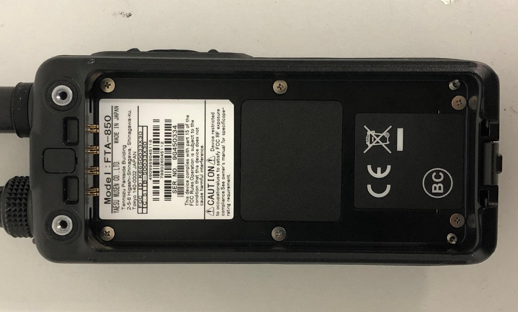
K6650033X30
Nov 18, 2020Airband Radio Transceiver
Equipment Class
TNF - Licensed Non-Broadcast Transmitter Held to Face