K66VR-5000
Yaesu Musen Co., Ltd.
Click to zoom
Application Details
- Equipment Class
- CSR - Scanning Receiver
- Date of Grant
- Sep 25, 2000
- Application Purpose
- Original Equipment
- Date of Application
- Jun 14, 2000
- Frequency Range
- 894.00000000 - 960.00000000
- Company
- Yaesu Musen Co., Ltd.
- Country
- Japan
Documents & Files
Document Text
Text extracted from the exhibit documents filed with the FCC. Open a document above to read the original.
Users Manual
VR-5000 Operating Manual 1 Front Panel Controls & Switches (1) MAIN VOL/SQL Knob MAIN VOL Knob The inner MAIN VOL knob adjusts the audio volume of the MAIN receiver in the speaker or headphones. SQL Knob The outer SQL knob sets the signal level threshold at which MAIN receiver audio is muted (and the “BUSY” icon in the LCD turns off), in all mode. This is normally kept fully counter clockwise, except when scanning and during FM operation. (2) SUB VOL/TONE Knob SUB VOL Knob This inner SUB VOL knob adjusts the audio volume of the SUB receiver in the speaker or headphones. TONE Knob The outer TONE knob adjusts receiver audio characteristics. (3) PHONES Jack This 3-pin (“stereo”) miniature jack is used for connection to your headphones. When a plug is inserted into this jack, the internal (or external) speaker will be cut off. This jack’s impedance is optimized for use with 16Ω to 32 Ω headphone type. (4) PWR Knob This is a main on/off switch for the VR-5000. Press and hold this switch for one second to toggle the receiver’s power on and off. (5) LCD (Liquid Crystal Display) The upper half of the display consists of dot-matrix display for frequency readout and various icons representing enabled receiver features. The lower half contains a dot-matrix display for Band Scope viewing, menu programming, and alpha numeric name display etc. (6) Functions Keys [M/S(SUB SET)] Key Press this key momentarily, to toggle the operating VFO between MAIN VFO and VR-5000 Operating Manual 2 SUB VFO. Press this key after [F] key is pressed, to toggle the VFO link feature on and off. [BS(BS SET)] Key Press this key momentarily, to toggle the Band Scope feature on and off. Press this key after [F] key is pressed when the Band Scope is activated, activate the SUB VFO cursor which enable the SUB VFO tuning. [WIDTH(BS STEP)] Key Press this key momentarily, to select the Band Scope sweep width. Press this key after [F] key is pressed when the Band Scope is activated, select the Band Scope sweeping step. [SCAN(M-S SCAN)] Key Press this key momentarily, to activate the scanning. Press this key after [F] key is pressed, to activate the M-S Scanning. M-S Scan: The scanner activates between the MAIN VFO frequency and SUB VFO frequency. [PMS(PMS SET)] Key Press this key momentarily, to activate the Programmable Memory Scan. Press this key after [F] key is pressed, to enable the PMS memory programming. [CLR(PRI CLR)] Key Press this key momentarily, Press this key after [F] key is pressed, to disable the Priority. [V(DIM)] Key Press this key momentarily, to enable the display brightness setting. Press this key after [F] key is pressed, activates the optional FVS-1A Voice Synthesizer Unit which provides announcement of the operating frequency (with resolution to the displayed 100 Hz digit) for operators with vision impairments. (7) PS Key Press this key momentarily, to recalls the one of up to five PS (PreSet) memories for operation. Press and hold this key for one second, to store the operating parameters into consecutive PS memories. (8) Command Keys [MODE(ADRS)] Key Press this key momentarily, to select the operating (receiving) mode. VR-5000 Operating Manual 3 Press this key after [F] key is pressed, to select the recording field for the voice recorder (required the optional FVS-1A Voice Synthesize Unit) [COPY(REC)] Key Press this key momentarily, copy the SUB VFO data into the MAIN VFO. Press this key after [F] key is pressed, to start the voice recorder. [STEP(PLAY)] Key Press this key momentarily, to select the synthesizer steps to be used during VFO operation. Press this key after [F] key is pressed, to playback the voice recorder. [V/M(MW)] Key Press this key momentarily, to change the frequency control between the VFO and the Memory system. Press this key after [F] key is pressed, to store the frequency into memory. [BANK] Key Press this key momentarily, to select the memory bank. (9) τ(θ)/υ(π) Keys In the VFO mode, pressing either of these keys momentarily step (according to the DIAL knob’s step) the operating frequency down or up respectively. Pressing either of these keys after [F] key is pressed, steps down or up 10 MHz. In the Memory mode, pressing either of these keys momentarily step the Memory Channel down or up respectively. While the Band Scope is engaged, pressing either of these keys to move the Channel Marker. (10) Keypad This keypad is used for direct frequency entry during VFO operation. Secondary functions allow to control the VR-5000’s various features. (11) [F] Key This key is used to activate the “Alternate” command functions of the panel keys. If this key is pressed before one of the panel keys is pressed, the “Alternate” functions of the key will be enabled. (12) DSP Key Press this key momentarily, activate the optional DSP-1 Digital Signal Processing VR-5000 Operating Manual 4 Unit. (13) DIAL Knob This is the main tuning dial for the VR-5000. It is used for most tuning memory selection, and function setting tasks on the VR-5000. Rear Panel Connections (1) DC 13.5V Jack This is the DC power supply connection for the VR-5000. Connect the Supplied PA- 4A AC adapter to this jack. (2) MUTE Jack If using the VR-5000 with a transceiver, shorting this jack during transmit will mute receiver output and attenuate RF signal input. Check with information provided with your particular transceiver for proper connection. (3) ANT B Terminal Use these spring-loaded terminal connectors to connect a high-impedance antenna. (4) ANT Switch This switch selects antenna connected from either the ANT A jack or ANT B terminal. (5) ANT A Jack Connect the 50 Ω coaxial feed line to your low-impedance antenna here using a type-M (PL-259) connector. (6) EXT SP Jack This 2-contact mini phone jack provides receiver audio for an external loudspeaker with an impedance of 4 ~ 16 Ω. Inserting a plug in this jack disables the loudspeaker. (7) REC Jack This jack provides a constant level (??? mV @ ? Ω) audio output, which is unaffe…
Text truncated - open the document above for the full version.
Cover Letter(s)
June 1st, 2000 Federal Communications Commission Authorization and Evaluation Division, 7435 Oakland Mills Road Columbia, MD 21045 USA Re: VR-5000 (FCC ID: K66VR-5000) Gentlemen: A. Part 15.19 & 15.21 Compliance Statement Drawing: B. Part 15.19 & 15.21 Compliance Statement Drawing Location: IN OPERATION MANUAL (location on inside back cover) Sincerely, YAESU MUSEN CO., LTD. Mr. Tomiro Ohmoto General Manager of Export Department 1. Changes or modifications to this device not expressly approved Yaesu Musen could void the user’s authorization to operate this device. 2. This device complies with part 15 of the FCC rules. Operation is subject to the following two conditions; (1) This device may not cause harmful interference, and (2) this device must accept any interference including interference that may cause undesired operation. 3. The scanning receiver in this equipment is incapable of tuning, or readily being altered, by the user to operate within the frequency bands allocated to the Domestic public Cellular Telecommunications Service in the Part 22. 40mm 97mm
Cover Letter(s)
June 1st, 2000 Federal Communications Commission Authorization and Evaluation Division, 7435 Oakland Mills Road Columbia, MD 21045 USA Re: VR-5000 (FCC ID: K66VR-5000) Gentlemen: The scanner receiver equipment meets the requirements of the FCC Rules, 15.121(a). Compliance is achieved through the following methods: The scanner receiver in this equipment is incapable of tuning, or readily being altered, by the User to operate within the frequency bands allocated to theDomestic Public Cellular Telecommunications Service in Part 22. Blocking of the cellular frequencies is implemented in the firmware of the unit’s main control central processing unit (CPU). Coverage of 824 – 849 MHz and 869 – 894 MHzis completely blocked, since it is done in the microprocessor, and cannot be re-enabledby any user-accessible procedure, including diode, resistor, or jumper changes, nor byconnection of any external device such as a personal computer, nor by installation of any “special” enabling semiconductor device. Sincerely, YAESU MUSEN CO., LTD. Mr. Tomiro Ohmoto General Manager of Export Department
Parts List/Tune Up Info
VR-5000 Alignment The VR-5000 has been carefully aligned at the factory for the specified performance across the amateur band. Realignment should therefore not be necessary except in the event of a component failure.All component replacement and service should be performed only by an authorized Yaesu representative, or the warranty policy may be voided. The following procedures cover the sometimes critical and tedious adjustments that are not normally required once the transceiver has left the factory.However, if damage occurs and some parts are replaced, realignment may be required.If a sudden problem occurs during normal operation, it is likely due to component failure; realignment should not be done until after the faulty component has been replaced. We recommend that servicing be performed only by authorized Yaesu service technicians who are experienced with the circuitry and fully equipped for repair and alignment. Therefore, if a fault is suspected, contact the dealer from whom the transceiver was purchased for instructions regarding repair. Authorized Yaesu service technicians realign all circuits and make complete performance checks to ensure compliance with factory specifications after replacing any faulty components. Those who do undertake any of the following alignments are cautioned to proceed at their own risk. Problems caused by unauthorized attempts at realignment are not covered by the warranty policy. Also, Yaesu must reserve the right to change circuits and alignment procedures in the interest of improved performance, without notifying owners. Under no circumstances should any alignment be attempted unless the normal function and operation of the transceiver are clearly understood, the cause of the malfunction has been clearly pinpointed and any faulty components replaced, and the need for realignment determined to be absolutely necessary. The following test equipment (and thorough familiarity with its correct use) is necessary for complete realignment. Correction of problems caused by misalignment resulting from use of improper test equipment is not covered under the warranty policy. While most steps do not require all of the equipment listed, the interactions of some adjustments may require that more complex adjustments be performed afterwards. Do not attempt to perform only a single step unless it is clearly isolated electrically from all other steps. Have all test equipment ready before beginning, and follow all of the steps in a section in the order presented. Required Test Equipment 1. RF Signal Generator with calibrated output level at 1000 MHz 2. AF Millivoltmeter 3. SINAD Meter 4. Regulated DC Power Supply: adjustable from 10 to 17 VDC, 5A 5. Frequency Counter: >0.1 ppm accuracy at 500 MHz 6. AF Signal Generator 7. DC Voltmeter: high impedance 8. AF Dummy Load: 8 ohm, 5W 9.Oscilloscope Alignment Preparation & Precautions Correct alignment requires that the ambient temperature be the same as that of the receiver and test equipment, and that this temperature be held constant between 20 and 30 C (68 86F). When the receiver is brought into the shop from hot or cold air it should be allowed some time for thermal equalization with the environment before alignment. If possible, alignments should be made with oscillator shields and circuit boards firmly affixed in place. Also, the test equipment must be thoroughly warmed up before beginning. Note: Signal levels in dB referred to in this procedure are based on 0 dBu = 0.5 uV(closed circuit). PLL Set up the test equipment as shown for alignment. Maintain the supply voltage at 13.8V DC for all steps. PLL VCV (Main VCO) 1) Connect the positive lead of the DC voltmeter to the test point TP2011(VCV) on the RF Unit, as indicated in the figure, and the negative lead to chassis ground. 2) Set the receiver to the 312.900 MHz, and adjust coil L2076 on the Unit for 7 V on the voltmeter. 3) Next tune to 1.000 MHz and confirm about 1.0 V on the voltmeter. 4) Set the receiver to the 621.900 MHz, and adjust coil L2098 on the Unit for 7 V on the voltmeter. 5) Next tune to 313.000 MHz and confirm about 1.0 V on the voltmeter. PLL VCV (Sub VCO) 1) Connect the positive lead of the DC voltmeter to the test point TP2010(VCV) on the RF Unit, as indicated in the figure, and the negative lead to chassis ground. 2) Set the receiver to the 2599.900 MHz, and adjust coil L2053 on the Unit for 6.5 V on the voltmeter. 3) Next tune to 4.900 MHz and confirm about 2.0 V on the voltmeter. PLL Reference Frequency The frequency counter connected to J2010, and while tuned to 1.000 MHz, and adjust TC2001 on the RF Unit, if necessary, so the counter frequency is within 100 Hz of 568.245 MHz. Receiver Set up the test equipment as shown below for receiver alignment. Interstage Transformers 1) While tuned to 101.000 MHz ,and the RF signal generator turned to the same frequency, set the generator for 3.5 kHz deviation with 1kHz tone modulation,and set the output level for 10 dBuV at the antenna jack. 2) Adjust CV3001 & CV3002 on the IF Unit for optimum SINAD,reducing the signal generator output level as necessary for proper meter deflection. 3) After the previous step, the final signal generator levelshould be less –3dBu for 12 dB SINAD. S-Meter Calibration 1) While tuned to 51.000 MHz,and turn the radio off. Press the [PWR] and [SACN] of the panel and hold while you turn the radio on. The radio now is in the Alignment Mode. 2) The [SCAN] buttons on the panel to select the “MAIN S-METER 1”,and press the [ENT] button. 3) The RF signal generator turned to the same frequency, set the generator for 3.5 kHz deviation with 1kHz tone modulation,and set the output level for -5dBu at the antenna jack, press the [ENT] button. 5) The [SCAN] buttons on the panel to select the “MAIN S-METER 5”,and press the [ENT] button. 6) The RF signal generator turned to the same frequency, set the generator for 3.5 kHz deviation with 1kHz tone modulation,and set the output level for +28d…
Text truncated - open the document above for the full version.
Parts List/Tune Up Info
LocationTypeNomenclatureApplication VR-5000 Component Application D 2001DIODEDAN235U TLSW D 2002DIODEDAN235U TLSW D 2004DIODEHVU355TRFBPF D 2005DIODEHVU355TRFBPF D 2006DIODE1SS355PROTECT D 2007DIODEHVM17BPF D 2008VARISTORMA28T-ALOCAL OSC D 2009DIODE1SS355PROTECT D 2010DIODE1SS355PROTECT D 2011DIODEHVU355BPF D 2012DIODEHVU355BPF D 2013DIODEHVM17BPF D 2014DIODEHVU359LOCAL OSC D 2015DIODEHVU359LOCAL OSC D 2016DIODE1SS355PROTECT D 2017DIODE1SS318SW D 2018DIODE1SS318SW D 2019DIODEDAN235USW D 2020DIODEDAN235USW D 2021DIODEDAN235USW D 2022DIODE1SS318SW D 2023DIODE1SS318SW D 2024DIODEHVU350REF. OSC D 2025DIODEHVU350REF. OSC D 2026DIODEHVU359BPF D 2027DIODEHVU359BPF D 2028DIODEHVR100BPF D 2030DIODEHVM17BPF D 2031DIODEHVM17BPF D 2032DIODE1SS355LOCAL OSC D 2033DIODESVC341LBPF D 2034DIODEHVU359BPF D 2035DIODEHVU355VCO D 2036DIODEHVU359BPF D 2037DIODEHVM17BPF D 2038DIODEHVR100BPF D 2039DIODEHVM17BPF D 2040DIODESVC341LBPF D 2041DIODEDAN235USW D 2042DIODEDAN235USW D 2043DIODE1SS318SW D 2044DIODE1SS318SW D 2045DIODE1SS318SW D 2046DIODE1SS318SW D 2047DIODE1SS318SW D 2048DIODE1SS318SW D 2049DIODE1SS318SW D 2050DIODE1SS355CONTROL D 2051DIODEHVU355VCO D 2052DIODE1SS355CONTROL D 2053DIODEHVU359VCO D 2054DIODE1SS318SW D 2056DIODEDAN235USW D 2057DIODEHVU355VCO LocationTypeNomenclatureApplication VR-5000 Component Application D 2058DIODE1SS318SW D 2059DIODEHVU355VCO D 2060DIODEDAN235USW D 2061DIODEHVU355VCO D 2062DIODE1SS355CONTROL D 2063DIODE1SS318SW D 2064DIODEDAN235USW D 2065DIODEDAN202KCONTROL D 2066DIODEDAN202KCONTROL D 2067DIODEDAN235USW D 2070DIODEDAN202KATT D 2071DIODEDAN202KSW D 2072DIODEDAN235USW D 2073DIODEDAN235USW D 2074DIODE21DQ04PROTECT D 2075SURGE ABSORBERDSP201M-S00BPROTECT D 2076DIODE1SS270PLL SUBSYSTEM D 2077DIODE1SS270PLL SUBSYSTEM Q 2001ICM5223AFPBPF TUNE Q 2002ICM5223AFPPLL SUBSYSTEM Q 2003ICM5223AFPPLL SUBSYSTEM Q 2004TRANSISTORDTC114EKPLL SUBSYSTEM Q 2005TRANSISTORDTC114EKCONTROL Q 2006TRANSISTOR2SC4116GRBUFF Q 2007TRANSISTOR2SC4116GRBUFF Q 2008TRANSISTORIMD3CONTROL Q 2009TRANSISTORDTC114EKCONTROL Q 2010TRANSISTORDTC114EKPLL SUBSYSTEM Q 2011ICNJM78L09UAREG Q 2012ICNJM78L05UAREG Q 2013ICUPC2711TBUFF Q 2014TRANSISTORDTC114EKCONTROL Q 2015TRANSISTORDTC114EKCONTROL Q 2016FET2SK210GRBUFF Q 2017ICL78M05TREG Q 2018ICMB15A02PFV1-GPLL SUBSYSTEM Q 2019FET3SK228XRSW Q 2020FET3SK228XRSW Q 2021FET3SK228XRSW Q 2022TRANSISTOR2SC4116GRREF. OSC Q 2023TRANSISTOR2SC4116GRLOCAL OSC Q 2024ICNJM78L09UAREG Q 2025ICUPC2711TRF AMP Q 2027TRANSISTOR2SC4116GRLOCAL OSC Q 2028TRANSISTOR2SC4116GRTEMP. CONTROL Q 2029TRANSISTOR2SA1586YTEMP. CONTROL Q 2030TRANSISTOR2SC3356VCO Q 2031FET3SK228XRSW Q 2032FET3SK228XRSW Q 2033FET3SK228XR1st MIX Q 2034TRANSISTOR2SC35851st MIX Q 2035TRANSISTOR2SC3356VCO Q 2036ICUPC2711TBUFF Q 2037TRANSISTOR2SA1586YPLL SUBSYSTEM LocationTypeNomenclatureApplication VR-5000 Component Application Q 2038ICNJU7201U30PLL SUBSYSTEM Q 2039TRANSISTORFMC3CONTROL Q 2040TRANSISTOR2SC3356VCO Q 2041TRANSISTOR2SC3356PLL SUBSYSTEM Q 2042TRANSISTORFMC3CONTROL Q 2043TRANSISTORFMC3CONTROL Q 2044TRANSISTORFMC3CONTROL Q 2045FET3SK228XRAGC Q 2047TRANSISTOR2SC3356VCO Q 2048TRANSISTORFMC3CONTROL Q 2049TRANSISTORFMC3CONTROL Q 2050TRANSISTORFMC3CONTROL Q 2051TRANSISTORFMC3CONTROL Q 2052TRANSISTOR2SC3356VCO Q 2053TRANSISTORFMC3CONTROL Q 2054TRANSISTORFMC3CONTROL Q 2055ICMB15E05PFV1PLL SUBSYSTEM Q 2056TRANSISTOR2SC35851st MIX Q 2058TRANSISTORFMC3CONTROL Q 2059ICBU4094BCFVCONTROL Q 2060TRANSISTORFMC3CONTROL Q 2061TRANSISTOR2SC3120BUFF Q 2062ICNJM78L09UAREG Q 2063ICUPC2711TBUFF Q 2064FET3SK228XR1st MIX Q 2065TRANSISTORFMC3CONTROL Q 2066TRANSISTORFMC3CONTROL Q 2067TRANSISTOR2SC3356VCO Q 2068ICUPC2710TBUFF Q 2069TRANSISTORFMC3CONTROL Q 2070TRANSISTOR2SC3356VCO Q 2071TRANSISTORDTC114EKCONTROL Q 2072ICBU4094BCFVCONTROL Q 2073TRANSISTORFMS1CONTROL Q 2074TRANSISTORFMS1CONTROL Q 2075ICUPC2711TBUFF Q 2076TRANSISTORFMC3CONTROL Q 2077TRANSISTORDTC114EKCONTROL Q 2078TRANSISTORDTC114EKPLL SUBSYSTEM Q 2079TRANSISTORFMS1ATT Q 2080TRANSISTOR2SC3420GRPROTECT D 3002DIODEHVU359LOCAL OSC D 3003DIODEHVU359LOCAL OSC D 3004VARISTORMA28T-ALOCAL OSC D 3005DIODEHVU355BUFF D 3007DIODEDA204KLIMITTER D 3008DIODE1SS355LOCAL OSC D 3009DIODEHVU355VCO D 3010DIODE1SS355NOISE BLANKER D 3011DIODEHVU355BUFF D 3012DIODEDAN202KSW D 3013DIODE1SS355NOISE BLANKER D 3014DIODEDA204KNOISE BLANKER [IF-UNIT] LocationTypeNomenclatureApplication VR-5000 Component Application D 3015DIODEDAN202KCONTROL D 3016DIODEDA204KBUFF D 3017DIODEDAN202KCONTROL D 3018DIODE1SS355SW D 3019DIODE1SS355SW D 3020DIODE1SS355SW D 3021DIODEDAN202KSW D 3022DIODE1SS355SW D 3023DIODE1SS355SW D 3024DIODE1SS355SW D 3025DIODE1SS355SW D 3026DIODE1SS355SW D 3027DIODE1SS355SW D 3028DIODEDA204KSCAN FILTER D 3029DIODEDA204KBUFF D 3030DIODEDAN202KCONTROL D 3031DIODE1SS355SW D 3032DIODE1SS355SW D 3033DIODE1SS355SW D 3034DIODE1SS355CONTROL D 3035DIODE1SS355CONTROL D 3036DIODE1SS355CONTROL D 3037DIODE1SS355CONTROL D 3038DIODE1SS355CONTROL Q 3001ICM5223AFPPLL SUBSYSTEM Q 3002ICM5223AFPBUFF Q 3003ICTC4W66FSW Q 3004ICNJM2902MBUFF Q 3005ICBU4066BFSW Q 3006ICM5223AFPCW/SSB AMP Q 3007TRANSISTOR2SC3120BUFF Q 3008TRANSISTOR2SC1623POWER SW Q 3009FET3SK228XRBUFF Q 3010TRANSISTOR2SB1134RPOWER SW Q 3011TRANSISTORDTC114EKPLL SUBSYSTEM Q 3012TRANSISTOR2SC4116GRBUFF Q 3013ICLA4425AAF PA Q 3014TRANSISTORFMW1 T98NOISE BLANKER Q 3015ICKIA7808APIREG Q 3016TRANSISTOR2SC3120BUFF Q 3017FET3SK228XR3rd MIX Q 3018ICMB15A02PFV1PLL SUBSYSTEM Q 3019TRANSISTOR2SC4116GRLOCAL OSC Q 3020TRANSISTORFMC3CONTROL Q 3021TRANSISTORFMC3CONTROL Q 3022TRANSISTORFMC3CONTROL Q 3023TRANSISTORFMC3CONTROL Q 3024TRANSISTORFMW1NOISE BLANKER Q 3025TRANSISTOR2SC2620QBBUFF Q 3026TRANSISTOR2SC2620QBSSB CARRIER Q 3027TRANSISTORDTC114EKCONTROL Q 3028ICBU4094BCFVCONTROL Q 3030TRANSISTOR2SC4116GRLOCAL OSC Q 3031TRANSISTORDTC114EKCONTROL LocationTypeNomenclatureApplication VR-5000 Component Application Q 3032FET3SK228XR2nd MIX Q 3033TRANSISTOR2SC2620QBCW/SSB AMP Q 3034TRANSISTORFMC3CONTROL Q 3035TRANSISTORFMC3CONTROL Q 3036TRANSISTORDTC114EKNOISE BLANKER Q 3037FET3S…
Text truncated - open the document above for the full version.
Test Report
FCC ID: K66VR-5000 MFA p0060005, d0060035 Date: June 15, 2000 Federal Communications Commission Via: Electronic Filing Attention: Authorization & Evaluation Division Applicant: Yaesu Musen Co., Ltd. Equipment: VR-5000 FCC ID: K66VR-5000 FCC Rules: 15.109, 15.121 Gentlemen: On behalf of the Applicant, enclosed please find Application Form 731, Engineering Test Report and all pertinent documentation, the whole for approval of the referenced equipment as shown. Filing fees are attached. We trust the same is in order. Should you need any further information, kindly contact the writer who is authorized to act as agent. Sincerely yours, Morton Flom, P. Eng. enclosure(s) cc: Applicant MF/cvr FCC ID: K66VR-5000 MFA p0060005, d0060035 CERTIFICATION of RECEIVER MODEL: VR-5000 FCC ID: K66VR-5000 to FEDERAL COMMUNICATIONS COMMISSION Part 15(B) (New) DATE OF REPORT: June 15, 2000 ON THE BEHALF OF THE APPLICANT: Yaesu Musen Co., Ltd. AT THE REQUEST OF : P.O. UPS 6/7/2000 Yaesu U.S.A. 17210 Edwards Rd. Cerritos, CA 90703 Attention of: Mikio Maruya, Executive Vice President (800) 255-9237; FAX: (800) 477-9237 (562) 404-2700, x280; FAX: -1210 [email protected] SUPERVISED BY: Morton Flom, P. Eng. FCC ID: K66VR-5000 MFA p0060005, d0060035 TABLE OF CONTENTS RULEDESCRIPTIONPAGE 2.948 Description of Measurement Facilities 1 15.109 Receiver Spurious Emissions (Radiated) 6 15.121(b) Scanning Receiver 11 15.107 A/C Powerline Conducted Emissions 13 FCC ID: K66VR-5000 MFA p0060005, d0060035 PAGE NO.1of17. Required information per ISO/IEC Guide 25-1990, paragraph 13.2: a) TEST REPORT b) Laboratory: (FCC: 31040/SIT) (Canada: IC 2044) M. Flom Associates, Inc. 3356 N. San Marcos Place, Suite 107 Chandler, AZ 85225 c) Report Number: d0060035 d) Client: Yaesu U.S.A. 17210 Edwards Rd. Cerritos, CA 90703 e) Identification: VR-5000 FCC ID: K66VR-5000 Description: Scanning Receiver f) EUT Condition: Not required unless specified in individual tests. g) Report Date: June 15, 2000 EUT Received: June 7, 2000 h, j, k): As indicated in individual tests. i) Sampling method: No sampling procedure used. l) Uncertainty: In accordance with MFA internal quality manual. m) Supervised by: Morton Flom, P. Eng. n) Results: The results presented in this report relate only to the item tested. o) Reproduction: This report must not be reproduced, except in full, without written permission from this laboratory. FCC ID: K66VR-5000 MFA p0060005, d0060035 PAGE NO.2of17. M. Flom Associates, Inc. is accredited by the American Association for Laboratory Association (A2LA) as shown in the scope below. "This laboratory is accredited by the American Association for Laboratory Accreditation (A2LA) and the results shown in this report have been determined in accordance with the laboratory's terms of accreditation unless stated otherwise in the report." Should this report contain any data for tests for which we are not accredited, or which have been undertaken by a subcontractor that is not A2LA accredited, such data would not covered by this laboratory's A2LA accreditation. FCC ID: K66VR-5000 MFA p0060005, d0060035 PAGE NO.3of17. GENERAL INFORMATION Part 2.948: (a)(b) DESCRIPTION OF MEASUREMENT FACILITIES: FILE: 31040/SIT A description of the measurement facilities was filed with the Commission and was found to be in compliance with the requirements of Section 2.948, by letter dated March 3, 1997. All pertinent changes will be reported to the Commission by up-date prior to March 2000. (b)(4) SUPPORTING STRUCTURES: SKETCH - ATTACHED EXHIBITS (b)(5)(6) TEST INSTRUMENTATION: LIST - SEE EXHIBITS 2.925: IDENTIFICATION OF AN AUTHORIZED DEVICE: DRAWING - SEE EXHIBITS LOCATION OF LABEL - SEE PHOTOS NAME AND ADDRESS OF APPLICANT : Yaesu Musen Co., Ltd. 4-8-8 Nakameguro, Meguro-Ku Tokyo 153-8644 Japan FCC ID: K66VR-5000 MFA p0060005, d0060035 PAGE NO.4of17. 2.911: 2.1033(b)(6) TECHNICAL REPORT MANUFACTURER: Yaesu Musen Co., Ltd. 4-8-8 Nakameguro, Meguro-Ku Tokyo 153-8644 Japan TRADE NAME: Yaesu FCC ID: K66VR-5000 MODEL NO: VR-5000 PHOTOGRAPHS : SEE LIST OF EXHIBITS 15.31: MEASUREMENT STANDARD & PROCEDURE: IEEE STANDARD 187 WAS USED AS A GUIDE. FCC MEASUREMENT PROCEDURE MP-1 x ANSI 63.4 (1992) “Methods of measurement od radio- noise emissions from low-voltage electrical and electronic equipment in the range of 9 kHz to 40 GHz.” FCC ID: K66VR-5000 MFA p0060005, d0060035 PAGE NO.5of17. EXPOSITORY STATEMENT 1. NUMBER OF BANDS = 1 2. NUMBER OF CHANNELS = 1200 3. TUNING RANGE, MHz = 0.1 to 2599.9 4. OSCILLATOR RANGE, MHz = 10.8 to 3215 5. I.F., MHz = 614, 45.775, 10.7 6. BLOCK DIAGRAM = ATTACHED 7. For cellular receiver only, the radio transceiver meets the requirements of FCC Bulletin OET 53 ("Cellular System Mobile Stations-Land-System Compatibility Specification."). See attached affidavit. 15.203 : ANTENNA REQUIREMENT: The antenna is permanently attached to the EUT The antenna uses a unique coupling The EUT must be professionally installed x The antenna requirement does not apply SUPERVISED BY: Morton Flom, P. Eng. FCC ID: K66VR-5000 MFA p0060005, d0060035 PAGE NO.6of17. NAME OF TEST: Receiver Spurious Emissions (Radiated) SPECIFICATION: 15.109: Radiated Interference Limits 15.33: Frequency Range of Radiated Measurements 80.217: Suppression of Interference Aboard Ships GUIDE: See measurement procedure below TEST CONDITIONS: Standard Temperature & Humidity TEST EQUIPMENT: As per attached page SEARCH ANTENNAS: 100 Hz - 50 MHz: Emco 3301B Active Rod 10 kHz - 32 MHz: Singer 94593-1 Loop 25 MHz - 300 MHz: Emco 3109 Biconical 200 MHz - 1 GHz: Aprel 2001 Log Periodic 1 GHz - 18 GHz: Emco 3115 Horn 10 GHz - 40 GHz: Emco 3116 Horn with HP11970A Mixer MEASUREMENT PROCEDURE 1. At first, bench tests were performed to locate the spurious emissions at the antenna terminals. 2. In the field, tests were conducted over the range shown, The test sample was set up on a wooden turntable above ground, and at a distance of three meters from the antenna connected tot he Spectrum Analyze…
Text truncated - open the document above for the full version.
Test Report
FCC ID: K66VR-5000 MFA p0060005, d0080084 PAGE NO.10 of 17. ADDENDUM August 23, 2000 NAME OF TEST: Receiver Spurious Emissions (Radiated) g0080573: 2000-Aug-21 Mon 14:45:00 STATE: 0:General All other emissions in the required measurement range were more that 20 dB below the required limits. FREQUENCY TUNED, MHz FREQUENCY EMISSION, MHz LEVEL, dBuV @ m C.F., dB μV/m @ m 622.000000 567.231000 10.93 3 25.86 69.1 3 931.000000 568.271000 9.38 3 25.9 58.08 3 1240.000000 569.241000 9.12 3 25.93 56.56 3 622.000000 1134.480000 3.78 3 34.14 78.7 3 931.000000 1136.512000 3.92 3 34.16 80.17 3 1240.000000 1138.502000 0.14 3 34.19 52.06 3 SUPERVISED BY: Morton Flom, P. Eng.
Test Report
FCC ID: K66VR-5000 MFA p0060005, d0090041 PAGE NO.15 of 17. AMENDED September 20, 2000 TEST SETUP: A/C Powerline Conducted Emissions g0090294: 2000-Sep-20 Wed 09:42:54 STATE: 0:General TEST SETUP: A/C Powerline Conducted Emissions g0090295: 2000-Sep-20 Wed 09:42:54 STATE: 0:General FCC ID: K66VR-5000 MFA p0060005, d0090041 PAGE NO.16 of 17. AMENDED September 20, 2000 NAME OF TEST: A/C Powerline Conducted Emissions g0090298: 2000-Sep-20 Wed 09:39:00 STATE: 0:General NEUTRAL SIDE SUPERVISED BY: Morton Flom, P. Eng. FCC ID: K66VR-5000 MFA p0060005, d0090041 PAGE NO.17 of 17. AMENDED September 20, 2000 NAME OF TEST: A/C Powerline Conducted Emissions g0090298: 2000-Sep-20 Wed 09:39:00 STATE: 0:General LINE SIDE SUPERVISED BY: Morton Flom, P. Eng.
Contact Information
Applicant
Masatoshi Muraishi(Engineering Division)
Technical Contact
M. Flom Associates, Inc.Morton Flom
[email protected]480 926 3100
3356 N. San Marcos Pl., Suite 107 · Chandler, Arizona · United States
Non-Technical Contact
M. Flom Associates, Inc.Morton Flom
[email protected]480 926 3100
Test Firm
M. Flom Associates, Inc.Morton Flom
Technical Specifications
| # | Rule Parts | Frequency Range | Power Output |
|---|---|---|---|
| 3 | 15B | 894 MHz - 960 MHz | - |
Other Applications from Yaesu Musen Co., Ltd.
K660E180X10
Dec 01, 2025BLUETOOTH MICROPHONE
Equipment Class
DTS - Digital Transmission System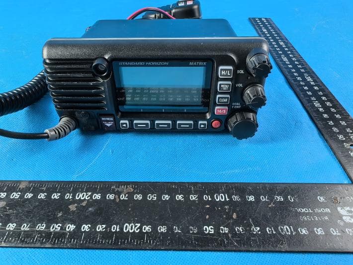
K6630673Y3D
Aug 01, 2024VHF FM Marine Transceiver
Equipment Class
CXX - Communications Rcvr for use w/ licensed Tx and CBs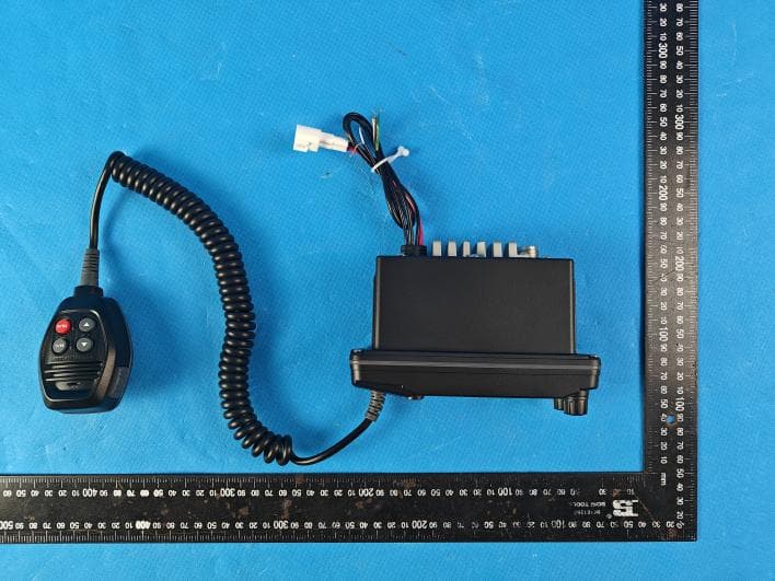
K6630653Y3D
Aug 01, 2024VHF FM Marine Transceiver
Equipment Class
CXX - Communications Rcvr for use w/ licensed Tx and CBs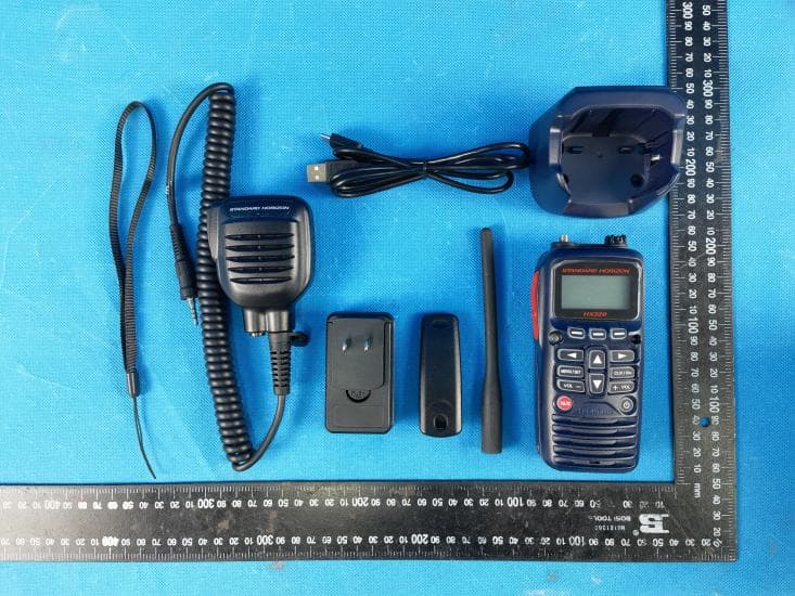
K6630683X30
Jan 10, 2023VHF FM Marine Transceiver
Equipment Class
TNF - Licensed Non-Broadcast Transmitter Held to Face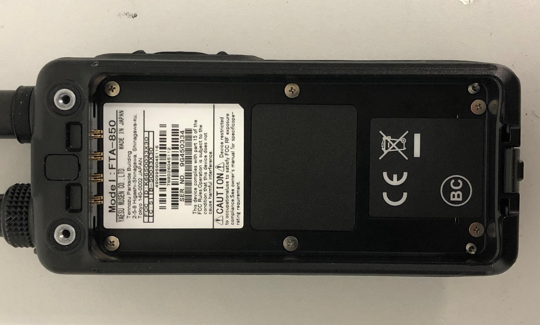
K6650033X30
Nov 18, 2020Airband Radio Transceiver
Equipment Class
TNF - Licensed Non-Broadcast Transmitter Held to Face