K66VX-1210HF Band Single Sideband Transceiver
Yaesu Musen Co., Ltd.
Click to zoom
Application Details
- Equipment Class
- TNB - Licensed Non-Broadcast Station Transmitter
- Date of Grant
- Mar 29, 2000
- Application Purpose
- Original Equipment
- Date of Application
- Feb 24, 2000
- Equipment Note
- HF Band Single Sideband Transceiver
- Frequency Range
- 1.70500000 - 30.00000000
- Company
- Yaesu Musen Co., Ltd.
- Country
- Japan
Documents & Files
Document Text
Text extracted from the exhibit documents filed with the FCC. Open a document above to read the original.
Users Manual
VX-1210 OPERATING MANUAL 1 Front Panel Control and Switches (1) POWER Switch Turn this knob clockwise (straight down) to turn the radio on. Counterclockwise rotation will turn the radio off. (2) SEL Knob This is 20-position detended rotary switch selects the memory channels or tunes the operating frequency. (3) VOL Knob This control adjusts the audio volume level. Clockwise rotation increases the volume level. (4) CLAR Knob This control allows you to offset the receiving frequency from that originally displayed (and used for transmission) frequency by up to 200 Hz in 10 Hz/step (SSB, CW, and DATA mode), or up to 400 Hz in 20 Hz step (AM mode). (5) GND Terminal If an earth ground connection point is available at the operating site, this terminal may be connected to it to provide improved performance and safety. (6) ANT Jack This jack accepts the 50Ω antenna. If an optional antenna tuner is installed, the optional whip antenna can be connecting to this connector directly. Use only type PL-259 (type M) plug. (7) SQL Switch Turn this switch to “upper” position to keep the receiver quiet until a signal is received. Turn this switch to “lower” position to “open” the noise squelch manually, allowing you to listen for very weak signals. This switch function can be customized, via programming by your dealer. See page XX for details regarding the available feature. (8) LAMP Switch Turn this switch to “upper” position to illuminate the LCD lamp continuously. To disable the LCD lamp, turn this switch to “lower” position. This switch function can be customized, via programming by your dealer. See page XX for details regarding the available feature. (9) LCD (Liquid Crystal Display) Display the current operating channel. (10) LED Indicator This LED indicates the current status of the transceiver. Glows Green: Busy Channel (or Squelch off) Glows Yellow: Transmission in progress Blinking Yellow: Blinking Red: Battery voltage is nearing depletion. Prepare to replace the battery. Glows Red: Battery voltage is critically low. Replace the battery immediately. VX-1210 OPERATING MANUAL 2 Rear Panel Connectors (1) CHG Terminal This 4-pin coaxial jack allows connection to the optional CD-17 Rapid Charger or PA-25 AC adapter. (2) Battery Compartment This compartment allows installation of the FNB-66LI Lithium-Ion Battery Pack. Before You Begin Battery Pack Installation and Removal To install the Battery Pack, insert the Battery Pack into the battery compartment on the bottom of the radio, then secure the Battery Pack using the screws on the Battery Pack. To remove the Battery Pack, turn the radio off and remove any protective cases. Unscrew the screws on the Battery Pack, then slide out the Battery Pack from the radio. (!) Do not attempt to open the Rechargeable Battery Pack, as personal injury or damage to pack could occur if a cell or cells become accidentally short-circuited. Battery Charging It is necessary to fully charge the Battery Pack before its first use. 1. Install the Battery Pack into the transceiver. Ensure that the transceiver is switched off. 2. Plug the CD-17 Charger into the AC line outlet. 3. Insert the cable plug from the CD-17 Charger into the CHG terminal on the bottom of the transceiver. A fully discharged pack will be charged completely in 5 hours. 4. Unplug the cable from the CHG terminal, then disconnect the CD-17 Charger from the AC line outlet. (!) Do not connect an improper Charger into the CHG terminal. Operation Preliminary Steps (1) Install a charged Battery Pack onto the transceiver, as described previously. (2) Connect the MH-50A7A Speaker/Microphone onto the transceiver; align the connector of the MH-50A7A to the connector on the left side of the transceiver body, then secure the connector pin using the screws supplied with the MH-50A7A Speaker/Microphone. (3) If you use this transceiver with the optional YA-30 antenna kit, setup the YA-30 antenna kit then connect the coaxial plug from the YA-30 onto the ANT jack of the transceiver. (4) If you use this transceiver with the optional YHA-61 whip antenna, connect the YHA-61 whip antenna onto the ANT jack of the transceiver then connect the good earth ground onto the GND terminal of the transceiver using heavy braided cable. Whip Antenna Setup (1) Connect the optional YHA-61 whip antenna and good ground earth onto the transceiver, as described previously. (2) Turn the transceiver on by rotating the POWER switch clockwise (set to straight VX-1210 OPERATING MANUAL 3 down) while press and holding the CHANNEL selector knob. Appear the “TU ADJ” in the display for three seconds, then return to the frequency display. (3) Press and hold the CHANNEL selector knob for 1/2 second to initiate antenna tuning. (4) Repeat step (3) on the all-operating channels. (5) Turn the transceiver off to save the new setting. Operation Quick Start (1) Turn the transceiver on by rotating the POWER switch clockwise. (2) Rotate the SEL knob to select the desired Memory Channel. (3) Rotate the VOL knob to set the comfortable volume level. (4) Turn the SQL switch (ANT side Toggle switch) to “upper” position to keep the receiver quiet until a signal is received. (5) To transmit, press and hold the microphone’s PTT switch, and speak into the microphone in a normal voice level. To return to the receive mode, release the PTT switch. (6) If you listen a very weak signals, turn SQL switch to “lower” position to “open” the noise squelch manually. (7) If the station you are receiving should start to drift, rotate the CLAR knob to follow the drifting signal without requiring you to move your transmit frequency. (8) In the night time operation, turn the LAMP switch (LCD side Toggle switch) to “upper” position to illuminate the LCD display. FUNCTION Switch Functions The VX-1210’s Function (Toggle) switches are determined to LAMP on/off (LCD side), HI/LOW switch (Center), and SQL off (ANT side) on default. Therefore, these switches functions can be customized, via programming…
Text truncated - open the document above for the full version.
Operational Description
VX-1210 Circuit Description 1 VX-1210 Circuit Description Receive Signal Path Incoming RF signal from the ANT jack is delivered to J3005 on the PA Unit, and passes through the ANT relay RL3014 and TX/RX relay RL3013 to the low-pass filter consists of the coils L3016 & L3017 and capacitors C3050, C3051, & C3052 which cut-off frequency is 30 MHz. The RF signal is then applied to J1001 on the MAIN Unit, and passed through the limitter circuit consist of D1001 , D1002 , D1003 , and D1004 (all 1SS244 ) to prevent the distortion from the high RF input and one of six band-pass filters which strip away unwanted signals to the RF amplifier Q1001 and Q1002 (both 2SK520-K41 ). The amplified RF signal is applied to the double balanced mixer D1009 ( HSB88WS ) where the RF signal is mixed with 1st local signal delivered from buffer Q1005 ( 2SC2954 ), resulting in a 47.055 MHz 1st IF signal. The 47.055 MHz 1st IF signal is fed through the monolithic crystal filter XF1001 ( 47M15AU ) which strip away unwanted mixer products, and then the 1st IF signal is applied to the 2nd mixer Q1006 ( 3SK151GR ), where it is mixed with the 36.355 MHz 2nd local signal delivered from buffer amplifier Q2038 ( 2SC2714Y ) on the Control Unit, resulting in a 10.7 MHz 2nd IF signal. The 10.7 MHz 2nd IF signal is fed through the Noise Blanker Gate D1014 & D1015 (both 1SS302 ) and 2nd IF filter XF1002 ( 10M2.4D ) to the 2nd IF amplifier Q1007 , Q1008 , & Q1009 (all 3SK151GR ). A portion of the 2nd IF signal is amplified by Q1011 & Q1012 (both 3SK151GR ), and then detected (with twofold voltage amplitude) by diode D1016 ( HSM198S ). This detected output controls the gain of above-mentioned FET by an average AGC voltage responsible for AGC amplifier Q1013 ( 2SK2812 ). Also, noise pulse contained in the detected output is amplified by the Q1014 ( 2SC2812 ) to be utilized for controlling Noise Blanker Gate D1014 & D1015 . In SSB, CW and FSK modes, the amplified 2nd IF signal from Q1009 is applied to the product detector diode D1024 & D1025 (both HSM198S ). In AM mode, the amplified 2nd IF signal from Q1009 is fed through the buffer amplifier Q1015 ( 2SC2812 ) and AM detector diodes D1021 & D1022 (both HSM198S ), then applied to the buffer amplifier Q1019 ( 2SC2812 ). The audio signal from the selected detector is fed through the low-pass filter Q1020 ( 2SC2812 ), which eliminates high-pitched noise on the audio signal, and amplified by AF preamplifier Q1023 ( M5218AFP ). The audio signal is then fed through the AF mute gate Q1025 ( TC4S66F ) and front panel AF potentiometer VR4001 , then back to audio amplifier Q1027 ( TDA2822D ) and Q1058 ( TDA7235 ). A portion of the output of AM detector diodes D1021 & D1022 is amplified by AGC amplifier Q1016 ( 2SC2812 ). The amplified DC voltage is fed through the buffer amplifier Q1018 ( 2SC2812 ) to the RF amplifier Q1001 & Q1002 and also the amplified DC voltage is fed to the 2nd gates of the IF amplifiers Q1007 , Q1008 , & Q1009 , to reduce their gain when strong signals are present in the receiver passband. When pulse type noise is received, a sample of the 2nd IF signal from Q1006 is amplified by Q1011 & Q1012 (both 3SK151GR ) before application to pulse detector D1016 ( HSM198S ). The resulting DC pulse switches noise blanker gate controller Q1014 ( 2SC2812 ), which interrupts the 2nd IF signal at noise blanker gate D1014 & D1015 during the length of the noise pulse. The DC voltage from the pulse detector is also amplified by Q1013 ( 2SC2812 ) and fed back to 2nd gates of the AGC amplifier Q1011 & Q1012 as noise blanker AGC. VX-1210 Circuit Description 2 Transmit Signal Path The speech audio from the microphone is delivered to J8001 on the MIC-CONN Unit, then applied to the J2002 on the CNTL Unit. The speech audio is amplified by Q2046 ( NJM4558V ), then passed though the MIC gain potentiometer VR1001, and further amplified by Q1043 ( 2SC2812 ) before application to balanced modulator D1036 ( HSB88WS ). The modulator also receives 10.7 MHz carrier signal from buffer amplifier Q1022 ( 2SC2812 ). The modulated signal is delivered to the crystal filter XF1002 where is stripped unwanted sideband. The resulting 10.7 MHz single sideband signal is buffered by Q1045 ( 3SK151GR ) and then applied to single balanced mixer Q1046 ( 3SK151GR ) which receives 36.355 MHz local signal from buffer amplifier Q2038 on the CNTL Unit. In AM mode, the single balanced mixer Q1046 also receivers 10.7 MHz carrier signal from buffer amplifier Q1022 to resulting the double sideband (AM) signal. The resulting the 47.055 MHz IF signal is fed through the monolithic crystal filter XF1001 which strip away unwanted mixer products, and then amplified by Q1048 ( 3SK151GR ). The amplified IF signal is delivered to double balanced mixer D1009 , where it is mixed with the PLL local signal from the buffer amplifier Q1005 ( 2SC2954 ). The resulting the RF signal at the transmit frequency is fed through the TX amplifier Q1049 ( 2SC2714Y ) and buffer amplifier Q1050 ( 2SC3357 ), and then filtered by one of six bandpass filters to suppress out-of-band mixer products. The RF signal is then amplified by Q1051 ( 2SK2954 ) and delivered to PA Unit. On the PA Unit, the low-level RF signal from the Main Unit is amplified by pre-drive Q3501 ( 2SC2166 ), push-pull driver Q3502/Q3503 (both 2SC2166 ), and then push-pull final amplifier Q3504/Q3505 (both 2SC3133 ), which provides approximately 20 watts RF output power. The RF output from the final amplifier is fed through the one of six low-pass filters, sampling directional coupler T3001, and TX/RX relay RL3014 before delivery to the antenna jack. The sampling directional coupler senses forward and reverse power output, which is rectified by D3001/D3005 & D3002/D3006 (all 1SS106 ) respectively for return to the ALC and SWR sensing circuitry on the Main Unit. The DC voltages derived from forward and reverse power are applied in combination to op-amp Q1053 ( M5218AFP ), the output which is…
Text truncated - open the document above for the full version.
Parts List/Tune Up Info
VX-1210 Component Application
Parts List/Tune Up Info
VX-1210 Alignment 1 VX-1210 Alignment The VX-1210 is carefully aligned at the factory for the specified performance across the entire operating frequency range. Realignment should therefore not be necessary except in the event of a component failure. All component replacement and service should be performed only by an authorized Vertex Standard representative, or the warranty policy may be void. The following procedures cover the sometimes critical and tedious adjustments that are not normally required once the repeater has left the factory. However, if damage occurs and some parts subsequently are placed, realignment may be required. If a sudden problem occurs during normal operation, it is likely due to component failure; realignment should not be done until after the faulty component has been replaced. We recommend that servicing be performed only by authorized Vertex Standard service technicians who are experienced with the circuitry and fully equipped for repair and alignment. Therefore, if a fault is suspected, contact the dealer from whom the repeater was purchased for instructions regarding repair. Authorized Vertex Standard service technicians realign all circuits and make complete performance checks to ensure compliance with factory specifications after replacing any faulty components. Those who do undertake any of the following alignments are cautioned to proceed at their own risk. Problems caused by unauthorized attempts at realignment are not covered by the warranty policy. Also, Vertex Standard reserves the right to change circuits and alignment procedures in the interest of improved performance, without notifying owners. Under no circumstances should any alignment be attempted unless the normal function and operation of the repeater are clearly understood, the cause of the malfunction has been clearly pinpointed and any faulty components replaced, and realignment determined to be absolutely necessary. The following test equipment (and thorough familiarity with its correct use) is necessary for complete realignment. Correction of problems caused by misalignment resulting from use of improper test equipment is not covered under the warranty policy. While most steps do not require all of the equipment listed, the interactions of some adjustments may require that more complex adjustments be performed afterwards. Do not attempt to perform only a single step unless it is clearly isolated electrically from all other steps. Have all test equipment ready before beginning, and follow all of the steps in a section in the order presented. Required Test Equipment r RF Signal Generator with calibrated output level at 30 MHz r In-line Wattmeter with 5% accuracy at 30 MHz r 50 Ω RF Dummy Load with power rating 50W at 30MHz r 16 Ω RF Dummy Load with power rating 50W at 30MHz r Frequency Counter with 0.02ppm accuracy at 40MHz r AF Signal Generator r AC Voltmeter r DC Voltmeter: High input impedance r DC Ammeter r HF Sampling Coupler r IBM PC / compatible Computer with MS-DOS or later operating system r Yaesu ___ Connection Cable & ___ Channel/Alignment Diskette VX-1210 Alignment 2 Alignment Preparation & Precautions A 50 Ω RF Dummy Load and in-line wattmeter must be connected to the ANT jack in all procedures that call for transmission, except where specified otherwise. Correct alignment is not possible with an antenna. After completing one step, read the following step to determine whether the same test equipment will be required. If not, remove the test equipment (except dummy load and wattmeter, in connected) before proceeding. Correct alignment requires that the ambient temperature be the same as that of the repeater and test equipment, and that this temperature be held constant between 20º and 30 °C (68º ~ 86 °F). When the repeater is brought into the shop from hot or cold air, it should be allowed time to come to room temperature before alignment. Whenever possible, alignments should be made with oscillator shields and circuit boards firmly affixed in place. Also, the test equipment must be thoroughly warmed up before beginning. Note: Signal levels in dB referred to in the alignment procedure are based on 0dBμ = 0.5μV. Set up the test equipment as shown below, and apply 13.8V DC power to the transceiver. The VX-1210 must be programmed for use in the intended system before alignment is attempted. The frequency and other parameters are loaded from the file during the alignment process. In order to facilitate alignment over the complete switching range of the equipment it is recommended that the channel data first be uploaded and then stored to disk. Alignment Channel data should then be downloaded. The original data can be replaced at the end of the alignment process. PLL Alignment PLL Reference Frequency Alignment r Remove the coaxial plug from J2009 on the CNTL Unit, and connect the Frequency Counter to J2009. r Adjust TC2001 on the CNTL Unit for 36.355 MHz ±10 Hz on the frequency Counter. 2nd Local Output Level r Disconnect the Frequency Counter, and connect the RF millivoltmeter to J2009. r Confirm that the output level is 0 dBm ±2dB on the RF millivoltmeter. r Disconnect the RF millivoltmeter, and replace the plug into J2009. Carrier Output Level r Remove the coaxial plug from J2008 on the CNTL Unit, and connect the RF millivoltmeter to J2008. r Select the “VCO1 U” channel (8.99999 MHz, USB), and confirm that the output level is –5.5 dBm ±2 dB. r Disconnect the RF millivoltmeter, and replace the plug into J2008. VCO VCV Alignment r Connect the DC voltmeter to TP2005 on the CNTL Unit, and referring Table below, turn the transceiver to each channel listed. Then adjust the listed component for the required voltage or confirm that the correct voltage is present. VX-1210 Alignment 3 Tune to: Adjust or Confirm: For: “VCO1 U” channel (8.9999 MHz, USB) T2001 6.0 V ±0.1 V “VCO1 L” channel (0.50000 MHz, USB) Confirm 1.3 ~ 2.3 V “VCO2 U” channel (18.9999 MHz, USB) T2002 6.0 V ±0.1 V “VCO2 L” …
Text truncated - open the document above for the full version.
Test Report
FCC ID: K66VX-1210 MFA p0020020, d0020061 Date: February 25, 2000 Federal Communications Commission Via Electronic Filing Attention: Authorization & Evaluation Division Applicant: Yaesu Musen Co., Ltd. Equipment: VX-1210 FCC ID: K66VX-1210 FCC Rules: 90, 87 Gentlemen: On behalf of the Applicant, enclosed please find Application Form 731, Engineering Test Report and all pertinent documentation, the whole for approval of the referenced equipment as shown. Filing fees are attached. We trust the same is in order. Should you need any further information, kindly contact the writer who is authorized to act as agent. Sincerely yours, William H. Graff, Director of Engineering enclosure(s) cc: Applicant WHG/cvr FCC ID: K66VX-1210 MFA p0020020, d0020061 LIST OF EXHIBITS (FCC CERTIFICATION (TRANSMITTERS) - REVISED 9/28/98) APPLICANT: Yaesu Musen Co., Ltd. FCC ID: K66VX-1210 BY APPLICANT: 1. LETTER OF AUTHORIZATION 2. IDENTIFICATION DRAWINGS, 2.1033(c)(11) LABEL LOCATION OF LABEL COMPLIANCE STATEMENT LOCATION OF COMPLIANCE STATEMENT 3. PHOTOGRAPHS, 2.1033(c)(12) 4. DOCUMENTATION: 2.1033(c) (3) USER MANUAL (9) TUNE-UP/ALIGNMENT PROCEDURE (10) SCHEMATIC DIAGRAM (10) OPERATIONAL DESCRIPTION 5. PART 90.203(e) & (g) ATTESTATION BY M.F.A. INC. A. TESTIMONIAL & STATEMENT OF CERTIFICATION B. STATEMENT OF QUALIFICATIONS FCC ID: K66VX-1210 MFA p0020020, d0020061 Sub-part 2.1033(c): EQUIPMENT IDENTIFICATION FCC ID: K66VX-1210 NAMEPLATE DRAWING ATTACHED, EXHIBIT 1. LOCATION AS PER LABEL DRAWING(S) DATE OF REPORT February 25, 2000 SUPERVISED BY: William H. Graff, Director of Engineering FCC ID: K66VX-1210 MFA p0020020, d0020061 THE APPLICANT HAS BEEN CAUTIONED AS TO THE FOLLOWING: 15.21 INFORMATION TO USER. The users manual or instruction manual for an intentional radiator shall caution the user that changes or modifications not expressly approved by the party responsible for compliance could void the user's authority to operate the equipment. 15.27(a) SPECIAL ACCESSORIES. Equipment marketed to a consumer must be capable of complying with the necessary regulations in the configuration in which the equipment is marketed. Where special accessories, such as shielded cables and/or special connectors are required to enable an unintentional or intentional radiator to comply with the emission limits in this part, the equipment must be marketed with, i.e. shipped and sold with, those special accessories. However, in lieu of shipping or packaging the special accessories with the unintentional or intentional radiator, the responsible party may employ other methods of ensuring that the special accessories are provided to the consumer, without additional charge. Information detailing any alternative method used to supply the special accessories for a grant of equipment authorization or retained in the verification records, as appropriate. The party responsible for the equipment, as detailed in § 2.909 of this chapter, shall ensure that these special accessories are provided with the equipment. The instruction manual for such devices shall include appropriate instructions on the first page of text concerned with the installation of the device that these special accessories must be used with the device. It is the responsibility of the user to use the needed special accessories supplied with the equipment. FCC ID: K66VX-1210 MFA p0020020, d0020061 TABLE OF CONTENTS RULE DESCRIPTION PAGE . Test Report 1 2.1033(c) General Information Required 2 2.1033(c)(14) Rule Summary 5 . Standard Test Conditions and Engineering Practices 6 2.1046(a) Carrier Output Power (Conducted) 7 2.1047(a) SSB Modulation Characteristics - Frequency Response of Audio Modulating Circuit 9 2.1047(b) SSB Power Output Limiting 11 2.1049(c)(2) SSB Occupied Bandwidth J3E 13 2.1051 SSB Spurious Emissions at Antenna Terminals 28 2.1053(a) Field Strength of Spurious Radiation 36 2.1055(a)(1) Frequency Stability - Temperature Variation 39 2.1055(b)(1) Frequency Stability - Voltage Variation 42 2.202(g) Necessary Bandwidth and Emission Bandwidth 43 FCC ID: K66VX-1210 MFA p0020020, d0020061 PAGE NO. 1 of 43. Required information per ISO/IEC Guide 25-1990, paragraph 13.2: a) TEST REPORT b) Laboratory: (FCC: 31040/SIT) (Canada: IC 2044) M. Flom Associates, Inc. 3356 N. San Marcos Place, Suite 107 Chandler, AZ 85225 c) Report Number: d0020061 d) Client: Yaesu U.S.A. 17210 Edwards Rd. Cerritos, CA 90703 e) Identification: VX-1210 FCC ID: K66VX-1210 Description: HF Band Single Sideband Transceiver f) EUT Condition: Not required unless specified in individual tests. g) Report Date: February 25, 2000 EUT Received: February 22, 2000 h, j, k): As indicated in individual tests. i) Sampling method: No sampling procedure used. l) Uncertainty: In accordance with MFA internal quality manual. m) Supervised by: William H. Graff, Director of Engineering n) Results: The results presented in this report relate only to the item tested. o) Reproduction: This report must not be reproduced, except in full, without written permission from this laboratory. FCC ID: K66VX-1210 MFA p0020020, d0020061 PAGE NO. 2 of 43. LIST OF GENERAL INFORMATION REQUIRED FOR CERTIFICATION IN ACCORDANCE WITH FCC RULES AND REGULATIONS, VOLUME II, PART 2 AND TO 90, 87 Sub-part 2.1033 (c)(1): NAME AND ADDRESS OF APPLICANT: Yaesu Musen Co., Ltd. 20-2, Shimomaruko 1-chome Ota-ku Tokyo, Japan 146 MANUFACTURER: Applicant (c)(2): FCC ID: K66VX-1210 MODEL NO: VX-1210 (c)(3): INSTRUCTION MANUAL(S): PLEASE SEE ATTACHED EXHIBITS (c)(4): TYPE OF EMISSION: 2K40J3E (c)(5): FREQUENCY RANGE, MHz: 3 to 30 (c)(6): POWER RATING, Watts: 20 Switchable Variable x N/A (c)(7): MAXIMUM POWER RATING, Watts: 100 FCC ID: K66VX-1210 MFA p0020020, d0020061 PAGE NO. 3 of 43. Subpart 2.1033 (continued) (c)(8): VOLTAGES & CURRENTS IN ALL ELEMENTS IN FINAL R. F. STAGE, INCLUDING FINAL TRANSISTOR OR SOLID STATE DEVICE: COLLECTOR CURRENT, A = per manual COLLECTOR VOLTAGE, Vdc = per manual SUPPLY VOLTAGE, Vdc = 13.8 (c)(9): TUNE-UP PROCEDURE: PLEASE …
Text truncated - open the document above for the full version.
Test Report
FCC ID: K66VX-1210 MFA p0020020, d0030071 PAGE NO.41 of 43. AMENDED March 28, 2000 NAME OF TEST:Frequency Stability (Temperature Variation) g0030201: 2000-Mar-28 Tue 10:18:00 STATE: 0:General SUPERVISED BY: William H. Graff, Director of Engineering
Contact Information
Applicant
Masatoshi Muraishi(Engineering Division)
Technical Contact
M. Flom Associates, IncWilliam H Graff
[email protected]480 926 3100
3356 N. San Marcos Place · Chandler, Arizona · United States
Non-Technical Contact
M. Flom Associates, Inc.Morton Flom
[email protected]480 926 3100
Test Firm
M. Flom Associates, Inc.Morton Flom
Technical Specifications
| # | Rule Parts | Frequency Range | Power Output | Emission | Tolerance |
|---|---|---|---|---|---|
| 1 | 87,90 | 1.705 MHz - 30 MHz | 20 W | 2K70J3E | 50.0000000000 Hz |
Other Applications from Yaesu Musen Co., Ltd.
K660E180X10
Dec 01, 2025BLUETOOTH MICROPHONE
Equipment Class
DTS - Digital Transmission System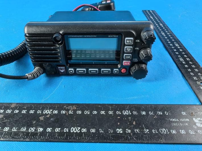
K6630673Y3D
Aug 01, 2024VHF FM Marine Transceiver
Equipment Class
CXX - Communications Rcvr for use w/ licensed Tx and CBs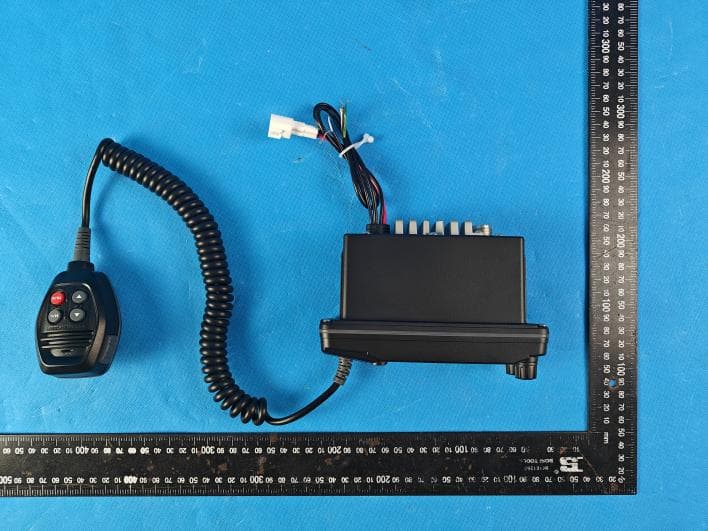
K6630653Y3D
Aug 01, 2024VHF FM Marine Transceiver
Equipment Class
CXX - Communications Rcvr for use w/ licensed Tx and CBs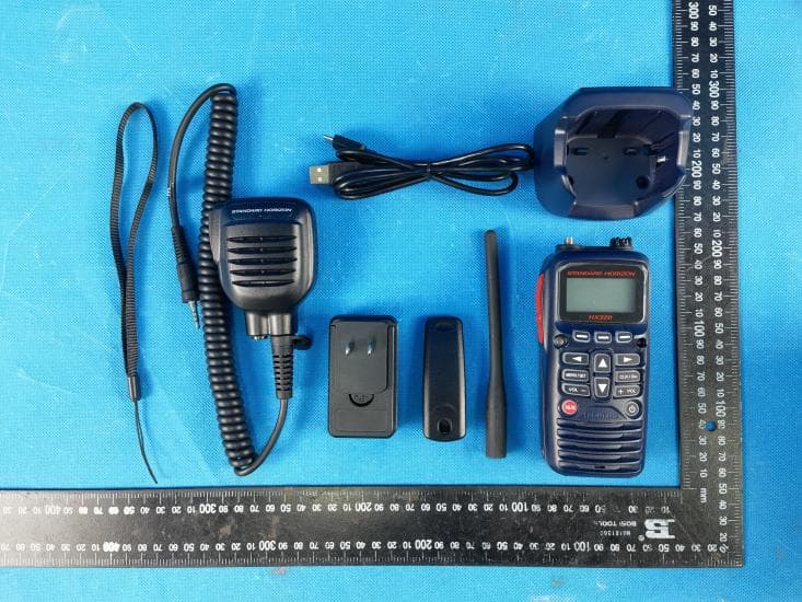
K6630683X30
Jan 10, 2023VHF FM Marine Transceiver
Equipment Class
TNF - Licensed Non-Broadcast Transmitter Held to Face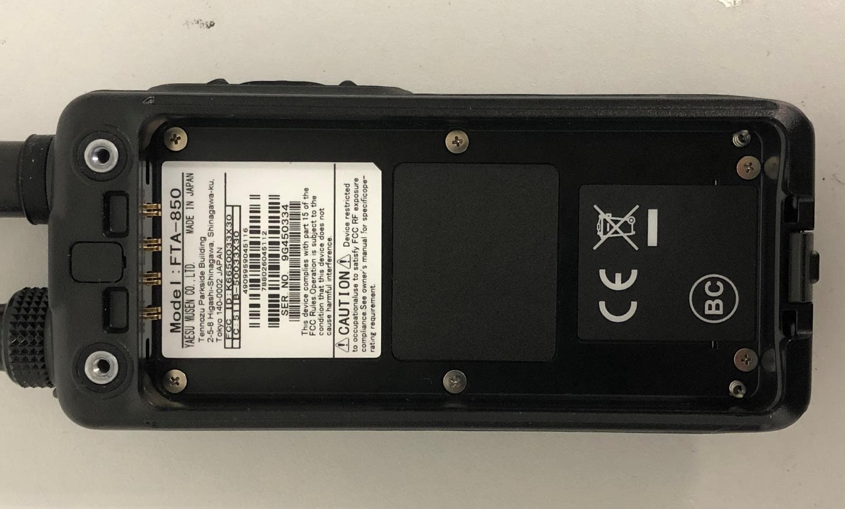
K6650033X30
Nov 18, 2020Airband Radio Transceiver
Equipment Class
TNF - Licensed Non-Broadcast Transmitter Held to Face