K66VX-210U-2UHF FM Handheld Transceiver
Yaesu Musen Co., Ltd.
Click to zoom
Application Details
- Equipment Class
- TNF - Licensed Non-Broadcast Transmitter Held to Face
- Date of Grant
- Nov 19, 2001
- Application Purpose
- Original Equipment
- Date of Application
- Sep 23, 2001
- Equipment Note
- UHF FM Handheld Transceiver
- Frequency Range
- 400.00000000 - 430.00000000
- Company
- Yaesu Musen Co., Ltd.
- Country
- Japan
Documents & Files
Document Text
Text extracted from the exhibit documents filed with the FCC. Open a document above to read the original.
Users Manual
VX-210A Operating Manual Controls & Connectors 0107Q-AE This device complies with Part 15 of the FCC rules. Operation is subject to the condition that this device does not cause harmful interference. Notice ! There are no owner-serviceable parts inside the transceiver. All service jobs must be referred to an authorized Service Representative. Consult your Authorized Dealer for installation of optional accessories. Microphone Speaker MIC/SP Jack ( External Mic/Earphone ) VOL/PWR Knob CH ( Channel ) Selector ACC Button Push To Talk ( PTT ) Switch Antenna LED Indicator Glows GreenACC on Blinking GreenBusy Channel (or SQL off) Glows RedTransmitting Blinking RedBattery Voltage is low Blinking YellowReceiving a Selective Call Battery Pack Latch Before You Begin rTo remove the battery, turn the radio off and remove any protective cases. Open the Battery Pack latch on the bottom of the radio, then slide the battery down- ward and out from the radio while holding the Belt Clip. Caution! Do not attempt to open any of the rechargeable Ni-Cd packs, as they could explode if accidentally short-circuited. Low Battery Indication rAs the battery discharges during use, the voltage gradually becomes lower. When the battery voltage reaches 6.3 volts, substitute a freshly charged battery and recharge the depleted pack. The TX/BUSY indicator on the top of the radio will blink red when the battery voltage is low. rAvoid recharging Ni-Cd batteries often with little use between charges, as this can degrade the charge capacity. We recommend that you carry an extra, fully- charged pack with you so the operational battery may be used until depletion (this “deep cycling” technique promotes better long-term battery capacity). Battery Pack Installation and Removal rTo install the battery, hold the transceiver with your left hand, so your palm is over the speaker and your thumb is on the top of the belt clip. Insert the battery pack into the battery compartment on the back of the radio while tilting the Belt Clip outward, then close the Battery Pack Latch until it locks in place with a “Click.” VOLCH 1 3 7 9 1 1 1 3 1 5 Preliminary Steps rInstall a charged battery pack onto the transceiver, as described previously. rScrew the supplied antenna onto the Antenna jack. Never attempt to operate this transceiver without an antenna connected. rIf you have a Speaker/Microphone, we recommend that it not be connected until you are familiar with the basic operation of the VX-210A. Operation Quick Start rTurn the top panel’s VOL/PWR knob clock- wise to turn on the radio on. rPull and turn the top panel’s CH selector knob to choose the desired operating channel. rRotate the VOL/PWR knob to set the volume level. If no signal is present, press and hold in the ACC button (the lower button on the left side) for more than 1 second (when “MONI- TOR” is assigned to the ACC button); back- ground noise will now be heard, and you may use this to set the VOL/PWR knob for the de- sired audio level. rPress and hold in the ACC button (when “MONITOR” is assigned to the ACC button) for more than 1 second (or press the ACC but- ton twice) to quiet the noise and resume normal (quiet) monitoring. Operation rTo transmit, press and hold in the PTT switch. Speak into the microphone area of the front panel grille (lower left-hand corner) in a nor- mal voice level. To return to the Receive mode, release the PTT switch. rIf a Speaker/Microphone is available, remove the plastic cap and its two mount- ing screws from the right side of the transceiver, then insert the plug from the Speaker/Microphone into the MIC/SP jack; secure the plug using the screws supplied with the Speaker/Microphone. Hold the speaker grille up next to your ear while receiving. To transmit, press the PTT switch on the Speaker/Micro- phone, just as you would on the main transceiver’s body. Note:Save the original plastic cap and its mounting screws. They should be re- installed when not using the Speaker/Microphone. Key Functions The VX-210A provides a programmable “ACC” (Accessory) button. The ACC button’s functions can be customized (set to any of a variety of functions), via pro- gramming by your VERTEX STANDARD dealer, to meet your communications/ network requirements. The particular function to be activated or disabled may re- quire a simple press of the ACC button, or it may require that the ACC button be pressed and held in for one second (or more). See the discussion below. Some features may require the purchase and installation of optional internal ac- cessories. The possible ACC button programming features are illus- trated below, and their func- tions are explained in the next chapter. For further details, contact your VERTEX STAN- DARD dealer. For future reference, check the box next to the function that has been assigned to the ACC button on your particular radio, and keep it handy. Function ACC button PressPress and Hold None Monitor Squelch OFF Low Power Scan Follow-me Scan Dual Watch Talk Around Call/Reset Speed Dial TX Save Off ACC 1 ACC 2 EC020U750 Monitor Press the ACC button to override (disable) the Tone Squelch. Background noise or incoming signals will now be heard whether or not a match- ing tone is present on the signal. Press the ACC button once more to resume normal (quiet) Tone Squelch action. Squelch OFF Press the ACC button to override both the Noise and Tone squelch systems. Again press the ACC button to resume normal (quiet) Noise and Tone squelch action. Low Power Press the ACC button to set the radio's transmitter to the “Low Power” mode, thus extending battery life. Press the ACC button again to return to “High Power” operation when in difficult terrain. Scan The Scanning feature is used to monitor multiple channels programmed into the transceiver. While scanning, the radio will check each channel for the presence of a signal, and will stop on a channel if a signal is present. rTo activate scanning: Press the ACC button. The scanner will search the chan…
Text truncated - open the document above for the full version.
External Photos
Front of EUT with Antenna Back of EUT with Antenna Front of EUT without Antenna Back of EUT without Antenna Right side of EUT Left side of EUT Top of EUT Bottom of EUT Top of Battery Charger Bottom of Battery Charger Top of AC Adapter Bottom of AC Adapter Front of Microphone Back of Microphone Antenna
ID Label/Location Info
VX-210AU VERTEX STANDARD CO., LTD. MADE IN JAPAN ******* CANADA: *** *** **** FCC ID: K66VX-210U-2 VERTEX STANDARD VX-210AU
Internal Photos
Back of without battery pack Battery pack Side-A of PCB Side-B of PCB with shield case Side-B of PCB without shield case Inside of front panel Inside back of chassis Inside top of battery charger Inside bottom of battery charger Component side of battery charger PCB Solder side of battery charger PCB Inside top of Battery charger chassis Inside bottom of battery charger chassis Inside of Microphone Inside of front microphone chassis Inside of back microphone chassis Inside of microphone
Operational Description
VX-210AU Circuit Description 1. Receive Signal Path Incoming RF from the antenna jack is delivered to the RF Unit and passes through a low-pass filter consisting of coils L1003, L1006 & L1007, capacitors C1002, C1007, C1013, C1017, C1022, C1025, C1029 & C1169, and antenna switching diode D1007 ( RLS135 ). Signals within the frequency range of the transceiver enter a varactor-tuned band- pass filter consisting of coils L1014 & L1015, capacitors C1057, C1058, C1064, C1071 & C1073, and diodes D1012 ( HVC355B ), D1013 ( 1SV280 ), D1016 ( HVC355B ) & D1017 ( 1SV280 ), then amplified by Q1015 ( 2SC5006 ) and enter a varactor-tuned band-pass filter consisting of coils L1021 & L1024, capacitor C1082, C1084, C1088,C1089,C1094, & C1096, and diodes, D1022 ( HVC355B ), D1023 ( 1SV280 ), D1024 ( HVC355B ), D1025 ( 1SV280 ),D1026 ( HVC355B ) & D1027 ( 1SV280 ), before first mixing by Q1025 ( SGM2016 ). Buffered output from the VCO is amplified by Q1009 ( 2SC5005 ) to provide a pure first local signal between 356.05 MHz and 386.05 MHz for injection to the first mixer Q1025. The 43.95 MHz first mixer product then passes through monolithic crystal filter XF1001 & XF1002 ( 43Y12B6 , 6.0 kHz BW) to strip away all but the desired signal, which is then amplified by Q1032 ( 2SC4215Y ). The amplified first IF signal is applied to FM IF subsystem IC Q1036 ( BA4116FV ), which contains the second mixer, second local oscillator, limiter amplifier, noise amplifier, and S-meter amplifier. A second local signal is generated by PLL reference/second local oscillator of 14.50 MHz crystal X1001 to produce the 450 kHz second IF when mixed with the first IF signal within Q1036. The second IF then passes through the ceramic filter CF1001 ( ALFYM450F=K ) or CF1002 ( SFPC450G : only on “Narrow” channels) to strip away unwanted mixer products, and is then applied to the limiter amplifier in Q1036, which removes amplitude variations in the 450kHz IF, before detection of the speech by the ceramic discriminator CD1001 ( CDBC450CX24 ). Detected audio from Q1036 is applied to the audio high-pass filter, and then passed via the volume control to the audio amplifier Q1039 ( TDA7233D ), which provides up to 0.5 Watts to the optional headphone jack or a 4-Ω loudspeaker. Squelch Control The squelch circuitry consists of a noise amplifier and band-pass filter within Q1036, and noise detector D1030 ( 1SS355 ). When no carrier received, noise at the output of the detector stage in Q1036 is amplified and band-pass filtered by the noise amplifier section of Q1036 and the network between pins 7 and 8, and then rectified by D1030. The resulting DC squelch control voltage is passed to pin 37 of the microprocessor Q1014 ( M37516E6HP ). If no carrier is received, this signal causes pin 7 of Q1014 to go high and pin 20 to go high. Pin 7 signals Q1037 ( RT1N441U ) to disable the supply voltage to the audio amplifier Q1039, while pin 20 hold the green (Busy) half of the LED off, when pin 7 is high and pin 20 is high. Thus, the microprocessor blocks output from the audio amplifier, and silences the receiver, while no signal is being received (and during transmission, as well). When a carrier appears at the discriminator, noise is removed from the output, causing pin 37 of Q1014 to go low and the microprocessor to activate the “Busy” LED via Q1014. The microprocessor then checks for CTCSS or CDCSS code squelch information, if enabled, or for DTMF data on the optional DTMF Unit. If not transmitting and CTCSS or CDCSS is not activated, or if the received tone or code matches that programmed, allows audio to pass through the audio amplifier Q1039 ( TDA7233D ) to the loudspeaker by enabling the supply voltage to it via Q1037. Transmit Signal Path Speech input from the microphone is amplified by Q1017 ( NJM2902V ), after pre- emphasis by C1059 and R1045, the audio passes another section of Q1017. The processed audio may then be mixed with a CTCSS tone generated by Q1014 ( M37516E6HP ) then delivered to D1005 ( HVU350 ) for frequency modulation of the PLL carrier (up to ±5kHz from the unmodulated carrier) at the transmitting frequency. If a CDCSS code is enabled for transmission, the code is generated by microprocessor Q1014 and delivered to D1004 ( 1SV230 ) for CDCSS modulating. If DTMF is enabled for transmission, the tone is generated by the microprocessor Q1014 and applied to the limitter amplifier section in place of the speech audio. Also, the tone is amplified for monitoring in the loudspeaker. The modulated signal from the VCO Q1005 ( 2SK508-K52 ) is buffered by Q1008 ( 2SC5005 ) and amplified by Q1009 ( 2SC5005 ). The low-level transmit signal is then passes through the T/R switching diode D1014 ( DAN235U ) to the driver amplifier Q1012 ( 2SC3357 ) and Q1016 ( 2SK2973 ), then amplified transmit signal is applied to the final amplifier Q1021( 2SK2974 ) up to 5 watts output power. The transmit signal then passes through the antenna switch D1007 ( RLS135 ) and is low-pass filtered to suppress harmonic spurious radiation before delivery to the antenna. 3-1 Automatic Transmit Power Control RF power output from the final amplifier is sampled by C1099, and is rectified by D1029 ( 1SS321 ). The resulting DC is fed back through Q1027 ( FMW1 ) to the drive amplifier Q1016 and final amplifier Q1021, for control of the power output. The microprocessor selects “High” or “Low” power levels. 3-2 Transmit Inhibit When the transmit PLL is unlocked, pin 7 of PLL chip Q1004 goes to a logic “low.” The resulting DC unlock control voltage is passed to pin 24 of the microprocessor Q1014. While the transmit PLL is unlocked, pin 22 of Q1014 remains high, which then turns off Q1031 and the Automatic Power Controller Q1027 ( FMW1 ) to disable the supply voltage to the drive amplifier Q1012, Q1016 and final amplifier Q1021, thereby disabling the transmitter. 3-3 Spurious Suppression Generation of spurious products by the transmitter is minimized by the fundamental carrier fre…
Text truncated - open the document above for the full version.
Parts List/Tune Up Info
VX-210AU COMPONENTS APPLICATION VX-210AU COMPONENTS APPLICATIONVX-210AU COMPONENTS APPLICATION VX-210AU COMPONENTS APPLICATION Address AddressAddress Address Device name Device nameDevice name Device nameDescription DescriptionDescription DescriptionApplication ApplicationApplication Application D 1001Varactor Diode HVC355BVCO Frequency Control D 1002Varactor Diode HVC355BVCO Frequency Control D 1003Diode HSU277 TRFTX/RX Switch D 1004Varactor Diode 1SV230 TPH3DCS Modulation D 1005Varactor Diode HVU350 TRFModulation D 1006Diode 1SS355 TE-17Temperature Control D 1007Diode RLS135 TE-11Antenna Switch D 1008Diode 1SS355 TE-17Speed up D 1010Diode HSU277 TRFAntenna Switch D 1011Diode HSU277 TRFAntenna Switch D 1012Varactor Diode HVC355BRX tune D 1013Varactor Diode 1SV280(TPH3)RX tune D 1014Varactor Diode DAN235U TLTX/RX Switch D 1015Dual Diode MC-2850 -T11-1Protect D 1016Varactor Diode HVC355BRX tune D 1017Varactor Diode 1SV280(TPH3)RX tune D 1018Diode 1SS355 TE-17Channel Switch D 1019Diode 1SS355 TE-17Channel Switch D 1020Diode 1SS355 TE-17Channel Switch D 1021Diode 1SS355 TE-17Channel Switch D 1022Varactor Diode HVC355BRX tune D 1023Varactor Diode 1SV280(TPH3)RX tune D 1024Varactor Diode HVC355BRX tune D 1025Varactor Diode 1SV280(TPH3)RX tune D 1026Varactor Diode HVC355BRX tune D 1027Varactor Diode 1SV280(TPH3)RX tune D 1028LED BRPY1211F-TRIndicator D 1029Dual Diode 1SS321Power Detector D 1030Diode 1SS355 TE-17SQL Detector D 1031Dual Diode MC-2846 -T11-1AF Switch D 1032Dual Diode MC-2850 -T11-1Speed up D 1033Dual Diode MC-2848 -T11-1W/N Switch D 1034Dual Diode MC-2848 -T11-1W/N Switch D 1035Zener Diode PTZ TE25 15AProtect D 1036Dual Diode MC-2850 -T11-1IF Limit Q 1001FET 2SK209GR TE85RBuffer Q 1002Transistor RT1N441U-T11-1TX/RX Switch Q 1003Transistor RT1N441U-T11-1Modulation W/N Switch Q 1004IC MB15A01PFV1-G-BND-EFPLL IC Q 1005Transistor 2SK508-T2B K52VCO Q 1006Transistor 2SC4154-T11-1ERipple Filter Q 1007Transistor RT1N441U-T11-1Dcs Modulation W/N Switch Q 1008Transistor 2SC5005-T1RF Amp Q 1009Transistor 2SC5005-T1RF Amp Q 1010Transistor 2SA1586Y TE85RModulation Switch Q 1011IC BR93LC56F-E2EEPROM Q 1012Transistor 2SC3357 T2-RFTX RF Amp Q 1013Transistor RT1P441U-T11-1Clone Switch Q 1014ICM37516E6HP(NO PROG.)Main Microprocessor Q 1015Transistor 2SC5006-T1RX RF Amp Q 1016FET 2SK2973-T13TX RF Amp Q 1017Quadruple Op-amp NJM2902V-TE1Modulation Audio Amp Q 1018Transistor RT1N441U-T11-1Tone W/N Switch Q 1019Switch TC4W66FU TE12LModulation Switch,Audio Switch Q 1020Transistor RT1P441U-T11-1Tone Switch Q 1021FET 2SK2974-T11TX Power Amp Q 1022Transistor 2SC4154-T11-1ELPF Q 1023Dual Op-amp NJM12903R(TE1)Subaudio Amp Q 1024Transistor 2SC4154-T11-1ELED Switch Q 1025FET SGM2016AM-T7Mixer Q 1026Dual Transistor FMW1 T98TX5V Control Q 1027Dual Transistor FMW1 T98APC Q 1028Dual Transistor FMW1 T98Save5V Control Q 1029Transistor 2SB1132-T100-QSave5V Control Q 1030Quadruple Op-amp NJM2902V-TE1LPF,HPF Q 1031Transistor 2SB1132-T100-QTX5V Control Q 1032Transistor 2SC4215Y TE85RIF Amp Q 1033Transistor RT1N441U-T11-1H/L Switch Q 1034Transistor RT1N441U-T11-1RX5V Control Q 1035Transistor DTB123EK T146RX5V Control Q 1036IC BA4116FV-E2FM IC Q 1037Transistor RT1N441U-T11-1Audio Control Q 1038IC S-80735SN-DZ-T1Voltage Detector Q 1039IC TDA7233D-TRAudio Amp Q 1040IC TK11235BMCLRegulator Q 1041Transistor RT1N441U-T11-1W/N Switch Q 1042Transistor 2SA1586Y TE85RAudio Switch Q 1043Transistor RT1N441U-T11-1W/N Switch Q 1044Transistor RT1N441U-T11-1W/N Switch Q 1046Transistor RT1N441U-T11-1Tone W/N Switch Q 1047Transistor 2SC4154-T11-1EBuffer Q 1048Dual Transistor UMC5NSave Switch Q 1050Transistor 2SB1122S-TDAudio Control Q 1051Transistor 2SC4154-T11-1ELPF Q 1052Transistor RT1N441U-T11-1TX/RX Switch Q 1053Transistor RT1N441U-T11-1TX/RX Switch Q 1054Dual Transistor UMD3N_TRCharge pump Q 1055Switch TC4W66FU_TE12LRoopfilter TX/RX Switch Q 1056Transistor RT1N441U-T11-1TX/RX Switch 1/1
Parts List/Tune Up Info
1 VX-210AU VX-210AUVX-210AU VX-210AU Type-A Alignment Type-A AlignmentType-A Alignment Type-A Alignment The VX-210A has been carefully aligned at the factory for the specified performance across the frequency range specified for each version. Re-alignment should therefore not be necessary except in the event of component failure, or altering version type. All component replacement and service should only be performed by an authorized Vertex Standard representative, or the warranty policy may be void. Required Test Equipment Required Test EquipmentRequired Test Equipment Required Test Equipment Vertex Standard CT-42 Programming Cable with CE-45 Channel Programming Diskette RF Signal Generator with calibrated output level at 1GHz Deviation Meter (Linear Detector) AC Voltmeter SINAD Meter In-Line wattmeter with 5 % accuracy at 500 MHz Regulated DC Power Supply adjustable from 4 to 10 V, 3 A 50Ω Non-reactive Dummy Load: 10 W at 500 MHz Frequency Counter: ±0.2 ppm accuracy at 500 MHz AF Signal Generator DC Voltmeter: high impedance Before beginning alignment, connect the transceiver and PC using the CT-42 Programming Cable, and run the CE-45 Channel Programming Diskette, then download the EEPROM data from the transceiver to the computer. Then store this data in a disk file so that it can be uploaded when alignment is finished. You should find the corresponding data file on the computer disk for the transceiver version you are aligning, containing channel settings for the high edge, middle and low edge of the transceiver’s frequency range in channels 1, 2 and 3, respectively. Up-load this file to the transceiver. Low Band Edge (Channel 1): 400.000 MHz Band Center (Channel 2): 415.000 MHz High Band Edge (Channel 3): 430.000 MHz 2 PLL & Transmitter PLL & TransmitterPLL & Transmitter PLL & Transmitter Set up the test equipment as shown for transmitter alignment. Adjust the supply voltage to 7.V for all steps where not specified otherwise. PLL VCV (Varactor Control Voltage) Connect the DC voltmeter between TP03 on the chip side of the Main Unit and ground. Set the transceiver to CH 3 (high band edge), and adjust L1004 on the chip side of the Main Unit for 3.6 V ± 0.1 V on the voltmeter. Set the transceiver to CH 1 (low band edge), and confirm the low-end VCV is more than 0.8 V while transmitting, and also while receiving. PLL Reference Frequency Set the transceiver to CH 2 (band center), key the transmitter and adjust TC1001 on the component side of the Main Unit, if necessary, so the frequency counter displays the band center frequency ±100 Hz (for the version being aligned) when transmitting. Transmitter Output Power Set the transceiver to CH 2 (band center), and select high power output. Ensure that the supply voltage is precisely 7.5 V, then adjust VR1004 on the component side of the Main Unit (while the PTT switch is pressed) for 5.0 W on the wattmeter, and confirm that supply current remains below 2.0 A. Modulation Level Set the transceiver to CH 2 (band center), adjust the AF generator for 77 mV rms output at 1 kHz to the MIC jack. Press the PTT switch and adjust VR1002 on the component side of the Main Unit for a deviation of ±4.2 kHz (for 25 kHz steps), or ±2.1 kHz (for 12.5 kHz steps). Receiver ReceiverReceiver Receiver Set up the test equipment as shown for receiver alignment. Sensitivity Set the transceiver to CH 3 (high band edge), and the RF signal generator tuned to the same frequency, set the generator for ±3.0 kHz deviation with 1 kHz tone modulation, and set the output level for 40 μV at the antenna jack. 3 Adjust VR1001 on the component side of the Main Unit for optimum SINAD, and confirm that signal generator level should be better than –7 dBμ for 12 dB SINAD. RSSI Connect the DC voltmeter between TP43 on the component side of the Main Unit and ground. Set the transceiver to CH 2 (band center), and the RF signal generator tuned to the same frequency, set the generator for ±3.0 kHz deviation with 1 kHz tone moderation, and set the output level for 15 dBμ at the antenna jack. Adjust VR1005 on the component side of the Main Unit for 0.7 V ± 0.1 V on the voltmeter.
RF Exposure Info
CELLTECH RESEARCH INC. Test Report S/N: 082901-161K66 1955 Moss Court, Kelowna Date(s) of Tests: Sept. 04, 2001 B.C. Canada V1Y 9L3 FCC SAR Evaluation _________________________________________________________________________________________________________ © 2001 Celltech Research Inc. CERTIFICATE OF COMPLIANCE SAR EVALUATION This wireless portable device has been shown to be compliant for localized Specific Absorption Rate (SAR) for controlled environment / occupational exposure limits specified in ANSI/IEEE Std. C95.1-1992 and has been tested in accordance with the measurement procedures specified in ANSI/IEEE Std. C95.3-1999. I attest to the accuracy of data. All measurements were performed by me or were made under my supervision and are correct to the best of my knowledge and belief. I assume full responsibility for the completeness of these measurements and vouch for the qualifications of all persons taking them. Celltech Research Inc. certifies that no party to this application has been denied FCC benefits pursuant to Section 5301 of the Anti-Drug Abuse Act of 1988, 21 U.S.C. 853(a). Shawn McMillen General Manager Celltech Research Inc. Test Lab: CELLTECH RESEARCH INC. Testing and Engineering Lab 1955 Moss Court Kelowna, B.C. Canada V1Y 9L3 Phone: 250 - 860-3130 Fax: 250 - 860-3110 Toll Free: 1-877-545-6287 e-mail: [email protected] web site: www.celltechlabs.com Applicant Information: VERTEX STANDARD CO., LTD. 4-8-8 Nakameguro, Meguro-ku Tokyo 153-8644, Japan FCC ID: K66VX-210U-2 Model(s): VX-210AU EUT Type: Portable UHF PTT Radio Transceiver Modulation: FM (UHF Band) Tx Frequency Range: 400 - 430 MHz Conducted Power Tested: 4.7 W (400.00 MHz) 4.0 W (415.00 MHz) 4.5 W (429.95 MHz) FCC Rule Part(s): 2.1093; ET Docket 96-326 IC Rule Part(s): RSS-102 Issue 1 CELLTECH RESEARCH INC. Test Report S/N: 082901-161K66 1955 Moss Court, Kelowna Date(s) of Tests: Sept. 04, 2001 B.C. Canada V1Y 9L3 FCC SAR Evaluation _________________________________________________________________________________________________________ © 2001 Celltech Research Inc. TABLE OF CONTENTS 1.0 INTRODUCTION.................................................................. 1 2.0 DESCRIPTION OF EUT.......................................................... 1 3.0 SAR MEASUREMENT SYSTEM ............................................. 2 4.0 MEASUREMENT SUMMARY.................................................. 3-4 5.0 DETAILS OF SAR EVALUATION............................................ 5 6.0 EVALUATION PROCEDURES................................................. 5 7.0 SIMULATED EQUIVALENT TISSUES...................................... 6 8.0 TISSUE PARAMETERS......................................................... 6 9.0 SAR LIMITS........................................................................ 7 10.0 SYSTEM VALIDATION.......................................................... 7 11.0 SYSTEM SPECIFICATIONS.................................................... 8 12.0 PROBE SPECIFICATION....................................................... 9 13.0 GENERIC TWIN PHANTOM................................................... 9 14.0 DEVICE HOLDER................................................................. 9 15.0 TEST EQUIPMENT LIST........................................................ 10 16.0 MEASUREMENT UNCERTAINTIES........................................ 11 17.0 REFERENCES...................................................................... 12 APPENDIX A - SAR MEASUREMENT DATA........................................ 13 APPENDIX B - DIPOLE VALIDATION................................................ 14 APPENDIX C - PROBE CALIBRATION............................................... 15 APPENDIX D - SAR TEST SETUP PHOTOGRAPHS............................... 16 CELLTECH RESEARCH INC. Test Report S/N: 082901-161K66 1955 Moss Court, Kelowna Date(s) of Tests: Sept. 04, 2001 B.C. Canada V1Y 9L3 FCC SAR Evaluation _________________________________________________________________________________________________________ © 2001 Celltech Research Inc. VERTEX STANDARD FCC ID: K66VX-210U-2 1 Portable UHF PTT Radio Transceiver (400-430MHz) 1.0 INTRODUCTION This measurement report shows compliance of the VERTEX STANDARD Model: VX-210AU Portable UHF PTT Radio Transceiver FCC ID: K66VX-210U-2 with the regulations and procedures specified in FCC Part 2.1093, ET Docket 96-326 Rules (controlled exposure), and RSS-102 Issue 1 of Industry Canada for mobile and portable devices. The test procedures, as described in American National Standards Institute C95.1-1992 (1), FCC OET Bulletin 65, Supplement C (Edition 01-01) were employed. A description of the product and operating configuration, detailed summary of the test results, methodology and procedures used in the evaluation, equipment used, and the various provisions of the rules are included within this test report. 2.0 DESCRIPTION of Equipment Under Test (EUT) Rule Part(s) FCC 2.1093; ET Docket 96.326 IC RSS-102 Issue 1 Modulation FM EUT Type Portable UHF PTT Radio Transceiver Tx Frequency Range (MHz) 400 - 430 FCC ID K66VX-210U-2 Conducted Power Tested 4.7 W (400.00 MHz) 4.0 W (415.00 MHz) 4.5 W (429.95 MHz) Model No.(s) VX-210AU Antenna Type Helical Whip Serial No. Pre-production Power Supply 7.2VDC 700mAh Ni-Cd Battery Pack Front of EUT w/ Speaker/Mic Back Side of EUT Left Side of EUT Right Side of EUT Front Side of Leather Holster Left Side of Leather Holster Right Side of Leather Holster Back Side of Leather Holster CELLTECH RESEARCH INC. Test Report S/N: 082901-161K66 1955 Moss Court, Kelowna Date(s) of Tests: Sept. 04, 2001 B.C. Canada V1Y 9L3 FCC SAR Evaluation _________________________________________________________________________________________________________ © 2001 Celltech Research Inc. VERTEX STANDARD FCC ID: K66VX-210U-2 2 Portable UHF PTT Radio Transceiver (400-430MHz) 3.0 SAR MEASUREMENT SYSTEM Celltech Research SAR measurement facility utilizes the Dosimetric Assessment Syst…
Text truncated - open the document above for the full version.
Test Report
FCC ID: K66VX-210U-2 MFA p0180003, d0180087 Date of Report: Date of Submission: August 29, 2001 September 24, 2001 Federal Communications Commission Via: Electronic Filing Attention: Authorization & Evaluation Division Applicant: Vertex Standard Co., Ltd. Equipment: VX-210AU FCC ID: K66VX-210U-2 FCC Rules: 90 Gentlemen: On behalf of the Applicant, enclosed please find Application Form 731, Engineering Test Report and all pertinent documentation, the whole for approval of the referenced equipment as shown. Filing fees are attached. We trust the same is in order. Should you need any further information, kindly contact the writer who is authorized to act as agent. Sincerely yours, Morton Flom, P. Eng. enclosure(s) cc: Applicant MF/cvr FCC ID: K66VX-210U-2 MFA p0180003, d0180087 LIST OF EXHIBITS (FCCCERTIFICATION(TRANSMITTERS) - REVISED 9/28/98) APPLICANT: Vertex Standard Co., Ltd. FCC ID: K66VX-210U-2 BY APPLICANT: 1. LETTER OF AUTHORIZATION x 2. IDENTIFICATION DRAWINGS, 2.1033(c)(11) xLABEL xLOCATION OF LABEL xCOMPLIANCE STATEMENT xLOCATION OF COMPLIANCE STATEMENT 3. PHOTOGRAPHS, 2.1033(c)(12) x 4. DOCUMENTATION: 2.1033(c) (3) USER MANUAL x (9) TUNE UP INFO x (10) SCHEMATIC DIAGRAM x (10) CIRCUIT DESCRIPTION x BLOCK DIAGRAM x PARTS LIST x ACTIVE DEVICES x 5. PART 90.203(e) & (g) ATTESTATION x 6. MPE Report x BY M.F.A. INC. A. TESTIMONIAL & STATEMENT OF CERTIFICATION B. STATEMENT OF QUALIFICATIONS FCC ID: K66VX-210U-2 MFA p0180003, d0180087 TRANSMITTER CERTIFICATION of FCC ID: K66VX-210U-2 MODEL: VX-210AU to FEDERAL COMMUNICATIONS COMMISSION Rule Part(s) 90 DATE OF REPORT: August 29, 2001 ON THE BEHALF OF THE APPLICANT: Vertex Standard Co., Ltd. AT THE REQUEST OF : P.O. Email 8/14/2001 Vertex Standard USA Inc. 17210 Edwards Rd. Cerritos, CA 90703 Attention of: Mikio Maruya, Executive Vice President (800) 255-9237; FAX: (800) 477-9237 (562) 404-2700, x280; FAX: -1210 [email protected] SUPERVISED BY: Morton Flom, P. Eng. FCC ID: K66VX-210U-2 MFA p0180003, d0180087 THE APPLICANT HAS BEEN CAUTIONED AS TO THE FOLLOWING: 15.21 INFORMATION TO USER. The users manual or instruction manual for an intentional radiator shall caution the user that changes or modifications not expressly approved by the party responsible for compliance could void the user's authority to operate the equipment. 15.27(a) SPECIAL ACCESSORIES. Equipment marketed to a consumer must be capable of complying with the necessary regulations in the configuration in which the equipment is marketed. Where special accessories, such as shielded cables and/or special connectors are required to enable an unintentional or intentional radiator to comply with the emission limits in this part, the equipment must be marketed with, i.e. shipped and sold with, those special accessories. However, in lieu of shipping or packaging the special accessories with the unintentional or intentional radiator, the responsible party may employ other methods of ensuring that the special acces…
Text truncated - open the document above for the full version.
Contact Information
Applicant
Masatoshi Muraishi(Engineering Division)
Technical Contact
M. Flom Associates, IncMorton Flom
[email protected]480 926 3100
3356 N. San Marcos Pl., Suite 107 · Chandler, Arizona · United States
Non-Technical Contact
M. Flom Associates, Inc.Morton Flom
[email protected]480 926 3100
Test Firm
M. Flom Associates, Inc.Morton Flom
Technical Specifications
| # | Rule Parts | Frequency Range | Power Output | Emission | Tolerance |
|---|---|---|---|---|---|
| 4 | 9 | 400 MHz - 430 MHz | 4.7 W | 16K0F3E | 2.5 ppm |
Other Applications from Yaesu Musen Co., Ltd.
K660E180X10
Dec 01, 2025BLUETOOTH MICROPHONE
Equipment Class
DTS - Digital Transmission System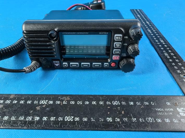
K6630673Y3D
Aug 01, 2024VHF FM Marine Transceiver
Equipment Class
CXX - Communications Rcvr for use w/ licensed Tx and CBs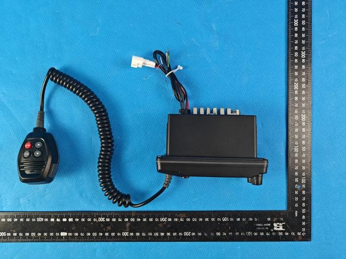
K6630653Y3D
Aug 01, 2024VHF FM Marine Transceiver
Equipment Class
CXX - Communications Rcvr for use w/ licensed Tx and CBs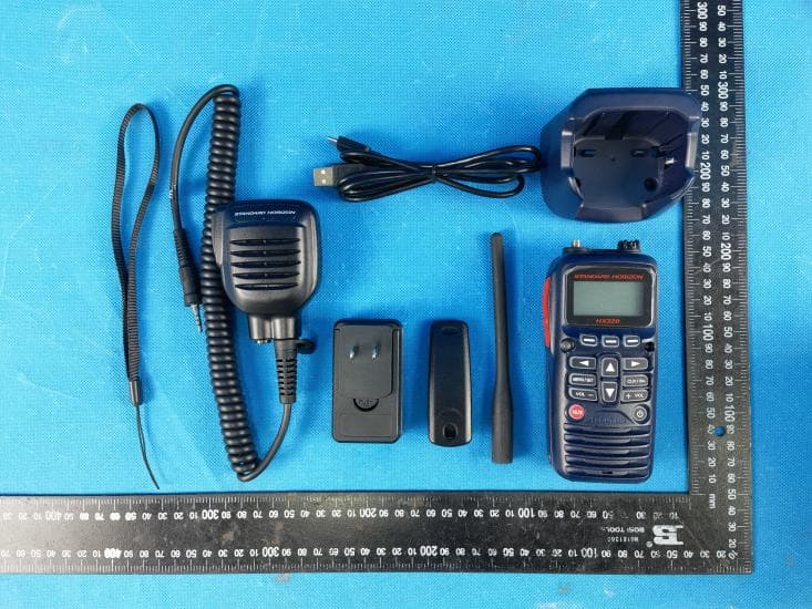
K6630683X30
Jan 10, 2023VHF FM Marine Transceiver
Equipment Class
TNF - Licensed Non-Broadcast Transmitter Held to Face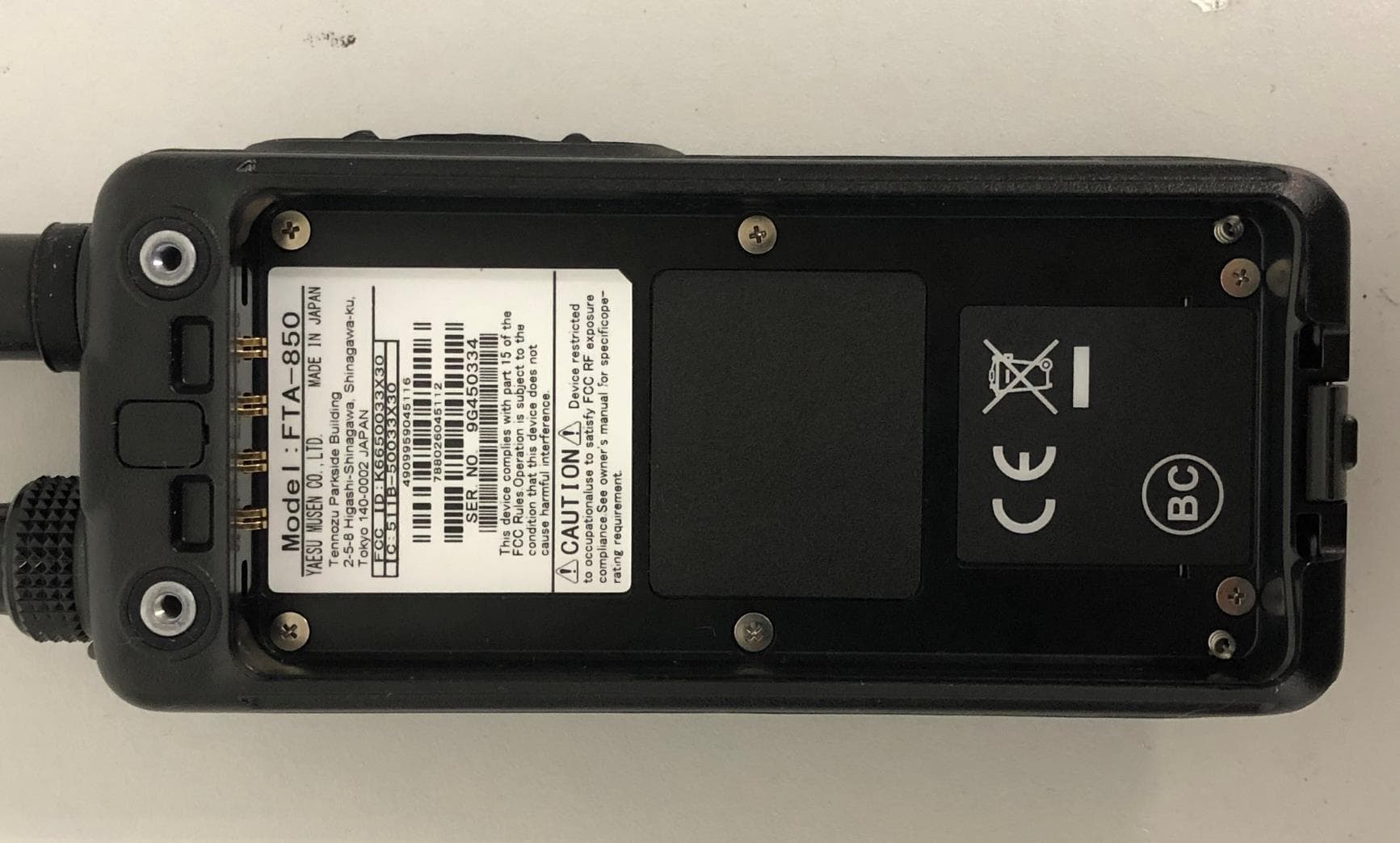
K6650033X30
Nov 18, 2020Airband Radio Transceiver
Equipment Class
TNF - Licensed Non-Broadcast Transmitter Held to Face