K66VX-3200V-2VHF FM Nonbroadcast Transceiver
Yaesu Musen Co., Ltd.
Click to zoom
Application Details
- Equipment Class
- TNB - Licensed Non-Broadcast Station Transmitter
- Date of Grant
- Jan 16, 2003
- Application Purpose
- Original Equipment
- Date of Application
- Jan 16, 2003
- Equipment Note
- VHF FM Nonbroadcast Transceiver
- Frequency Range
- 134.00000000 - 165.00000000
- Company
- Yaesu Musen Co., Ltd.
- Country
- Japan
Documents & Files
Document Text
Text extracted from the exhibit documents filed with the FCC. Open a document above to read the original.
Users Manual
VX-3200 OPERATING MANUAL VERTEX STANDARD CO., LTD. 4-8-8 Nakameguro, Meguro-Ku, Tokyo 153-8644, Japan VERTEX STANDARD US Headquarters 17210 Edwards Rd., Cerritos, CA 90703, U.S.A. International Division 8350 N.W. 52nd Terrace, Suite 201, Miami, FL 33166, U.S.A. YAESU EUROPE B.V. P.O. Box 75525, 1118 ZN Schiphol, The Netherlands YAESU UK LTD. Unit 12, Sun Valley Business Park, Winnall Close Winchester, Hampshire, SO23 0LB, U.K. VERTEX STANDARD HK LTD. Unit 5, 20/F., Seaview Centre, 139-141 Hoi Bun Road, Kwun Tong, Kowloon, Hong Kong VX-3200 OPERATING MANUAL VX-3200 OPERATING MANUAL Congratulations! You now have at your fingertips a valuable communications tool: a VERTEX STAN- DARD two-way radio! Rugged, reliable and easy to use, your VERTEX STANDARD radio will keep you in constant touch with your colleagues for years to come, with negligible maintenance downtime. Please take a few minutes to read this manual carefully. The information presented here will allow you to derive maximum performance from your radio, in case ques- tions arise later on. We’re glad you joined the VERTEX STANDARD team. Call on us anytime, because communications is our business. Let us help you get your message across. NOTICE ! There are no owner-serviceable parts inside the transceiver. All service jobs must be referred to an authorized VERTEX STANDARD Service Represen- tative. Consult your Authorized VERTEX STANDARD Dealer for installa- tion of optional accessories. SAFETY/WARNING INFORMATION WARNING - DO NOT operate the VX-3200 radio when any person(s) (by- standers) outside the vehicle are within the distances shown in the chart at the bottom of this section. Safety Training information: Antennas used for this transmitter must not exceed an antenna gain of 0 dBd. The radio must be used in vehicle-mount configurations with a maximum op- erating duty factor not exceeding 50%, in typical Push-to-Talk configurations. This radio is restricted to occupational use, work related operations only where the radio operator must have the knowledge to control the exposure condi- tions of its passengers and bystanders by maintaining the minimum separa- tion distance shown below. Failure to observe these restrictions will result in exceeding the FCC RF ex- posure limits. Antenna Installation: For rear deck trunk installation, the antenna must be located at least the fol- lowing distance away from rear-seat passengers and bystanders (outside vehicle) in order to comply with the FCC RF exposure requirements. For roof top installations, the antenna must be placed in the center of the roof. Radiated Frequency and Distance VX-3200VVX-3200U ( A ) VX-3200U ( D ) VX-3200U ( F ) 2.00 Feet 2.69 Feet 2.53 Feet 2.45 Feet ( 0.61 m ) ( 0.819 m ) ( 0.773 m ) ( 0.748 m ) VX-3200 OPERATING MANUALPage 1 INTRODUCTION For North American Users Regarding 406 MHz Guard Band The U.S. Coast Guard and National Oceanographic and Atmospheric Admin- istration have requested the cooperation of the U.S. Federal Communications Commission in preserving the integrity of the protected frequency range 406.0 to 406.1 MHz, which is reserved for use by distress beacons. Do not attempt to program this apparatus, under any circumstances, for operation in the fre- quency range 406.0 - 406.1 MHz if the apparatus is to be used in or near North America. The VX-3200 Series are full-featured FM transceivers designed for flexible mobile and base station business communications in the VHF or UHF Land Mobile bands. These transceiver are designed for reliable business communications in a wide vari- ety of applications with a wide range of operating capability provided by their lead- ing-edge design. The 128-channel memories can each be programmed with an 8-character channel name. Important channel frequency data is stored in EEPROM and flash memory on the CPU, and is easily programmable by dealers using a personal computer and the VER- TEX STANDARD VPL-1 Programming Cable and CE52 Software. The pages which follow will detail the many advanced features provided on the VX- 3200 transceiver. After reading this manual, you may wish to consult with your Net- work Administrator regarding precise details of the configuration of this equipment for use in your application VX-3200 OPERATING MANUALPage 2 CONTROLS & CONNECTORS Front Panel Important! - All buttons located on the Front Panel are Programmable Function ( PF ) Buttons, configured according to your network requirements and programmed by your VERTEX STANDARD dealer. The instructions below a typically-config- ured radio. VOL/PWR Knob Turn this control clockwise to turn the radio on and to increase the volume. Turn it counterclockwise into the click-stop to turn the radio off. BUSY/TX Indicator Indicate transceiver Transmit/Receive Status Steady Red:Transmitting in progress Steady Green:Busy Channel Blinking Green:Tone Squelch in defeated condition LCD (Liquid Crystal Display) The display includes an 8-character alpha-numeric section showing Group and Channel names, status and identity information, and error messages. VX-3200 OPERATING MANUALPage 3 [ q ] / [ p ] Buttons (Programmable Function Buttons) Pressing either button changes the current channel (and displayed channel num- ber or name). Holding a button for more than 1/2 second causes the function to repeat. Microphone Jack Connect the microphone plug to this jack. [A] Button (Programmable Function Button) This button can be set up for special applications, such as High/Low power se- lection, Monitor, Talk-Around, etc, as determined by your network requirements and programmed by your VERTEX STANDARD dealer. [s]/[r] Buttons (Programmable Function Buttons) Pressing either button changes the current group (and displayed group number or name). Holding a button for more than 1/2 second causes the function to repeat. [P1] - [P4] Buttons (Programmable Function Buttons) These buttons can be set up for special applications, such as High/Low power selection, Monitor, Talk-Around, etc, …
Text truncated - open the document above for the full version.
External Photos
FCC ID: K66VX-3200V-2 Vertex Standard Co., Ltd. Front view Rear view FCC ID: K66VX-3200V-2 Vertex Standard Co., Ltd. Left view Right view FCC ID: K66VX-3200V-2 Vertex Standard Co., Ltd. Top view Bottom view FCC ID: K66VX-3200V-2 Vertex Standard Co., Ltd. Microphone DC Power Cable
ID Label/Location Info
VX-3200V (Type A)VX-3200V (Type A) LABEL DRAWINGLABEL DRAWING Vertex Standard Co., Ltd.Vertex Standard Co., Ltd. (1:1) (1:2) ID / Part 15.19 and CAUTION drawings VX-3200V K66VX-3200V-2 ID drawing Part 15.19 and CAUTION drawings This device complies with part 15 of FCC Rules. Operation is subject to that this device dose not cause harmful interference. Device restricted to occupational use to satisfy FCC RF exposure compliance. See owner’s manual for specific operating requirement. VX-3200V K66VX-3200V-2 Label location CAUTION This device complies with part 15 of FCC Rules. Operation is subject to that this device dose not cause harmful interference. Device restricted to occupational use to satisfy FCC RF exposure compliance. See owner’s manual for specific operating requirement. CAUTION
Internal Photos
FCC ID: K66VX-3200V-2 Vertex Standard Co., Ltd. Side-A of RF-UNIT with shield cases Side-A of RF-UNIT without shield cases FCC ID: K66VX-3200V-2 Vertex Standard Co., Ltd. Side-B of RF-UNIT Inside front of panel with PWB FCC ID: K66VX-3200V-2 Vertex Standard Co., Ltd. Inside front of panel without PWB Side-A of PANEL-UNIT with LCD FCC ID: K66VX-3200V-2 Vertex Standard Co., Ltd. Side-A of PANEL-UNIT without LCD Side-B of PANEL-UNIT FCC ID: K66VX-3200V-2 Vertex Standard Co., Ltd. Front of LCD Back of LCD FCC ID: K66VX-3200V-2 Vertex Standard Co., Ltd. Inside of chassis Inside of microphone
Operational Description
FCC ID: K66VX-3200V-2 Circuit Description 1/3 Vertex Standard Co., Ltd. VX-3200V Circuit Description 1. Overview The VX-3200V is a VHF/FM mobile transceiver designed to operate in the frequency range of 134 to 165 MHz or 148 to 174 MHz. 2. Circuit Configuration by Frequency The receiver is a double-conversion superheterodyne with a first intermediate frequency (IF) of 44.25 MHz and a second IF of 450 kHz. Incoming signals from the antenna are mixed with the local signal from PLL to produce the first IF of 44.25 MHz. This is then mixed with the 44.25 MHz second local oscillator (using the 14.6 MHz reference crystal) output to produce the 450 kHz second IF. This is detected to give the demodulated signal. The transmit signal frequency is generated by PLL VCO, and modulated by the signal from the microphone. It is then amplified and sent to the antenna. 3. Receive Signal Path Incoming RF signals from the antenna connector are delivered to the RF Unit. RF signals pass through a low-pass filter (LPF) antenna switching network consisting of coils L1001, L1003, and L1005, capacitors C1004, C1008, C1009, and C1011, and antenna switching diodes D1005, D1007, and D1031, for delivery to the receiver front end. Signals within the frequency range of the transceiver are then passed through a varactor-tuned bandpass filter consisting of L1009 and L1014 before RF amplification by Q1011 (2SC3356). The amplified RF is then band-pass filtered again by varactor-tuned resonators L1026, and L1027 to ensure pure in-band input to 1st mixer Q1038 (GN2011-Q). Buffered output from the VCO Unit is amplified by Q1021 (2SC5107) and low- pass filtered by L1030 / L1031 and C1178 / C1180 / C1182, to provide a pure 1st local signal between 192.25 and 218.25 MHz to the 1st mixer. The 44.25 MHz 1st mixer product then passes through dual monolithic crystal filters XF1001 and XF1002 (± 5.5 kHz BW), and is amplified by Q1029 (2SC4215Y) and delivered to the input of the FM IF subsystem IC Q1028 (TA31136FN). This IC contains the 2nd mixer, 2nd local oscillator, limiter amplifier, FM detector, noise amplifier, and squelch gates. The 2nd LO in the IF-IC is produced from crystal X1001 (14.600 MHz) and the 1st IF is converted to 450 kHz by the 2nd mixer and stripped of unwanted components by ceramic filter CF1001 or CF1002. After passing through a limiter amplifier, the signal is demodulated by the FM detector CD1001 (CDBC450CX24). Detected audio from Q1029 is applied to Q2016(AK2345) and audio low-pass filter. After volume adjustment by Q2014(M62364FP), the audio signal is amplified by the AF power amplifier Q1509 (TDA2003H) and passed to speaker jack. 4. Transmit Signal Path Voice audio from the microphone is delivered via the Mic (Jack) Unit to the FCC ID: K66VX-3200V-2 Circuit Description 2/3 Vertex Standard Co., Ltd. PANEL Unit, after passing through amplifier Q2022 (NJM2902V), Mic gain- volume Q2014 (M62364FP) pre-emphasisQ2015 (NJM2902V), and limiter (IDC instantaneous deviation control), is adjusted for optimum deviation level and delivered to the next stage. Voice input from the microphone CTCSS, and DCS audio are modulated by the VCO , and the reference frequency oscillator of the synthesizer. Synthesizer output, after passing through diode switch D1022 (1SS321), is amplified by driver Q1025 (2SC5415E) / Q1026 (2SC5107-O) and power module Q1039 (RA60H1317M) to obtain full RF output. The RF energy then passes through antenna switch D1005 / D1007 / D1031 and a low-pass filter circuit and finally to the antenna connector. RF output power from the final amplifier is sampled by CM coupler and is rectified by D1011, D1012 (HSM88AS x 2). The resulting DC is fed through Automatic Power Controller Q1003 (NJM2902V), to transmitter RF amplifier and thus the power output. Generation of spurious products by the transmitter is minimized by the fundamental carrier frequency being equal to the final transmitting frequency, modulated directly in the transmit VCO. Additional harmonic suppression is provided by a low-pass filter consisting of L1001, L1003, L1004, L1027, C1004, C1009, C1011, C1151, and C1152, resulting in more than 60dB of harmonic suppression prior to delivery to the RF energy to the antenna. 5 PLL Frequency Synthesizer PLL frequency synthesizer consists of the VCO Q1013 (2SK508-K52:RX) and Q1015 (2SC5107-O:TX), VCO buffers Q1018 (2SC5107-O), Q1020 (2SC5107-O), Q1021 (2SC5107-O), PLL subsystem IC Q1023 (MA15A02PFV1) and 14.6 MHz reference crystal X1001. The frequency stability is ±2.5 ppm within temperature range of -30 to +60 °C. The output of the 14.6 MHz reference is applied to pin 1 of the PLL IC. While receiving, VCO Q1013 oscillates between 405.75 and 445.75 MHz according to the transceiver version and the programmed receiving frequency. The VCO generates 192.25 to 218.25MHz for providing to the first local signal. In TX, the VCO generates 148 to 174MHz. The output of the VCO is amplified by the Q1020 and routed to the pin 8 of the PLL IC. Also the output of the VCO is amplified by the Q1021 and routed first local /Power Module according to D1022. The PLL IC consists of a prescaler, fractional divider, reference divider and phase comparator and charge pump. This PLL IC is fractional-N type synthesizer and performs in the 40 or 50 kHz reference signal, which is eighth of the channel step (5 or 6.25 kHz). The input signal from pin 1 and 8 of the PLL IC is divided down to the 20kHz and compared at phase comparator. The pulsed output signal of the phase comparator is applied to the charge pump and transformed into DC signal in the loop filter. The DC signal is applied to the pin 1 of the VCO and locked to keep the VCO frequency constant. PLL data is output from DCS_E (pin100), CLOCK (pin2) and PLL_E (pin98) of the microprocessor Q2013. The data are input to PLL IC when the channel is changed or when transmission is changed to reception and vice versa. A PLL lock condition is always monitored by the pin20 of the Q2013. Whe…
Text truncated - open the document above for the full version.
Parts List/Tune Up Info
Documents for FCC FCC ID: K66VX-3200V-2 Vertex Standard Co., Ltd. Document for FCC Model Name: VX-3200V TypeFCC IDSerial number A, 134-165 MHzK66VX-3200V-22N000010 Documents for FCC FCC ID: K66VX-3200V-2 Vertex Standard Co., Ltd. EQUIPMENT SPECIFICATION DECLARED BY THE APPLICANT Model Name : VX-3200V FCC ID : K66VX-3200V-2 Specification is Referenced : EIA/TIA-603 Emission Type : 16K0F3E / 11K0F3E Channel Spacing : 25 / 12.5[KHz] Description : Mobile Mode : FM Frequency RangeATX : 134-165[MHz] RX : 134-165[MHz] Rated RF PowerHIGH : 50[W] LOW : 5[W] Maximum Power Rating : 300[W] Power Supply VoltageDC : 13.8[V] Collector Voltage : 13.8[V] Collector Current : 9.8[A] Documents for FCC FCC ID: K66VX-3200V-2 Vertex Standard Co., Ltd. VX-3200V Specifications General Frequency range(Type A):134-165 MHz (Type C):148-174 MHz Number of Groups32 Number of Channel250 channels Channel spacing:25 / 12.5 KHz Emission type:16K0F3E / 11K0F3E Power supply voltage(Rated):13.6 V DC Current consumption(RX @ 13.8V, 4W AF):500 mA (TX @ 45W):10 A Temperature range:-30 to +60 °C Case size(W x H x D):160 x 40 x 170 mm Weight(Approx.):1.4 Kg Receiver Circuit type:Double-conversion superheterodyne Ifs(1 st ):44.25 MHz (2 nd ):450 KHz 12dB SINAD Sensitivity0.25 μV Adjacent channel selectivity:85(25K) / 70(12.5K) dB Intermodulation:80 dB Spurious rejection:90 dB Speaker impedance:4 Ω AF Output(@ 4 Ω, 10 % THD)4 W Transmitter Power Output(High):50 W (Low):5 W Frequency stability:± 2.5 ppm Modulation system:Variable reactance Maximum deviation:5 / 2.5 KHz FM Noise:better than 45 / 40 dB Spurious emissions:better than 70 dB AF distortion(@ 1 KHz)5 % Microphone type:Dynamic Microphone impedance:600 Ω
Parts List/Tune Up Info
FCC ID: K66VX-3200V-2 Alignment 1/6 Vertex Standard Co., Ltd. VX-3200V Alignment Introduction The VX-3200V is carefully aligned at the factory for the specified performance across the frequency range specified for each version. Realignment should therefore not be necessary except in the event of a component failure, or altering version type. All component replacement and service should be performed only by an authorized Vertex Standard representative,or the warranty policy may be void. The following procedures cover the sometimes critical and tedious adjustments that are not normally required once the transceiver has left the factory. However, if damage occurs and some parts subsequently are placed, realignment may be required. If a sudden problem occurs during normal operation, it is likely due to component failure; realignment should not be done until after the faulty component has been replaced. We recommend that servicing be performed only by authorized Vertex Standard service technicians who are experienced with the circuitry and fully equipped for repair and alignment. Therefore, if a fault is suspected, contact the dealer from whom the transceiver was purchased for instructions regarding repair. Authorized Vertex Standard service technicians realign all circuits and make complete performance checks to ensure compliance with factory specifications after replacing any faulty components. Those who do undertake any of the following alignments are cautioned to proceed at their own risk. Problems caused by unauthorized attempts at realignment are not covered by the warranty policy. Also, Vertex Standard reserves the right to change circuits and alignment procedures in the interest of improved performance, without notifying owners. Under no circumstances should any alignment be attempted unless the normal function and operation of the transceiver are clearly understood, the cause of the malfunction has been clearly pinpointed and any faulty components replaced, and realignment determined to be absolutely necessary. The following test equipment (and thorough familiarity with its correct use) is necessary for complete realignment. Correction of problems caused by misalignment resulting from use of improper test equipment is not covered under the warranty policy. While most steps do not require all of the equipment listed, the interactions of some adjustments may require that more complex adjustments be performed afterwards. Do not attempt to perform only a single step unless it is clearly isolated electrically from all other steps. Have all test equipment ready before beginning, and follow all of the steps in a section in the order presented. Required Test Equipment RF Signal Generator with calibrated output level at 1000MHz Deviation Meter (linear detector) In-line Wattmeter with 5% accuracy at 1000MHz 50-Ω RF Dummy Load with power rating 100W at 1000MHz 4-Ω AF Dummy Load FCC ID: K66VX-3200V-2 Alignment 2/6 Vertex Standard Co., Ltd. Regulated DC Power Supply (standard 13.8V DC, 15A) Frequency Counter with 0.1ppm accuracy at 1000MHz AC Voltmeter DC Voltmeter VHF Sampling Coupler IBM PC / compatible Computer Oscilloscope Vertex Standard VPL-1 Connection Cable & Alignment program Alignment Preparation & Precautions A 50-Ω RF Dummy Load and in-line wattmeter must be connected to the main antenna jack in all procedures that call for transmission, except where specified otherwise. Correct alignment is not possible with an antenna. After completing one step, read the following step to determine whether the same test equipment will be required. If not, remove the test equipment (except dummy load and wattmeter, in connected) before proceeding. Correct alignment requires that the ambient temperature be the same as that of the transceiver and test equipment, and that this temperature be held constant between 20 and 30 ° C (68 - 86 ° F). When the transceiver is brought into the shop from hot or cold air, it should be allowed time to come to room temperature before alignment. Whenever possible, alignments should be made with oscillator shields and circuit boards firmly affixed in place. Also, the test equipment must be thoroughly warmed up before beginning. Note: Signal levels in dB referred to in the alignment procedure are based on 0dBμ EMF = 0.5μV. Setup the test equipment as shown for transceiver alignment,apply 13.8V DC power to the transceiver. Refer to the drawings above for Alignment Points. Fig.1 Alignment Setup VPL-1 cable J1502 Data port VX-3200 In-Line Wattmeter RF sampling coupler Deviation meter Frequency counter 50Ω Dummy Load 13.8Vdc power supply Signal generator Antenna Port Oscilloscope AF Generator Sinad Meter 4Ω Dummy Personal Computer See Fig 2 FCC ID: K66VX-3200V-2 Alignment 3/6 Vertex Standard Co., Ltd. (Fig 2: J1502 connection for the modulation adjustment) The transceiver must be programmed for use in the intended system before alignment is attempted. The RF parameters are loaded from the file during the alignment process. [Important] In order to facilitate alignment over the complete switching range of the equipment it is recommended that the channel data in the transceiver is preset as the chart below. Table.1 RF Ch. List Frequency(Simplex)RF Ch. listCh. Space Ver. AVer. C Ch 1 Wide147.100162.100MID Frequency(Wide) [use in the SVC47] Ch 2 Narrow147.100162.100MID Frequency(Narrow) [use in the SVC47 ] Ch 3 Wide134.100148.100LOW Frequency [for PLL VCV adjustment] Ch 4 Wide159.900173.900HIGH Frequency [for PLL VCV adjustment] The alignment mode is accessed by “Alignment mode” command from the computer whilst switching on. And it is operated by the alignment tool automatically. During the alignment mode, normal operation is suspended. Use the alignment tool program running on PC. ・PLL VCV Connect the positive lead of the DC voltmeter to the test point TP1007 (VCV) on the RF-Unit, as indicated in the figure, and the negative lead to chassis ground. Set the transceiver to the high…
Text truncated - open the document above for the full version.
Parts List/Tune Up Info
FCC ID: K66VX-3200V Component Applications Address Device nameDescriptionApplication BR008050* D 1001 DiodeRLS135 TE-11RF Limiting RF-UNITD 1002 DiodeBAS316RF Limiting D 1003 DiodeDSA3A1Reverse Voltage Protection D 1004 DiodeP6KA18Reverse Voltage Protection D 1005 DiodeUM9957F/TRAntenna Switch D 1006 DiodeBAS316APC Switch D 1007 DiodeUM9957F/TRAntenna Switch D 1008 Varactor DiodeHVU306A5TRFBPF Tune D 1009 DiodeBAS316APC D 1010 Varactor DiodeHVU306A5TRFBPF Tune D 1011 DiodeHSM88AS TRPower Detector D 1012 DiodeHSM88AS TRPower Detector D 1013 Varactor DiodeHVU306A5TRFRX VCO D 1014 Varactor DiodeHVU306A5TRFRX VCO D 1015 Varactor DiodeHVU306A5TRFTX VCO D 1016 Varactor DiodeHVU306A5TRFTX VCO D 1017 Varactor Diode1SV214 TPHTX MOD D 1018 Varactor DiodeHVU306A5TRFBPF Tune D 1019 Varactor DiodeHVU306A5TRFBPF Tune D 1020 Varactor DiodeHVU300A-TRTemp. Control for PLL REF D 1021 DiodeBAS316Un Lock D 1022 Diode1SS321 TE85RTx/Rx RF Switch D 1023 Varactor DiodeHVU359TRFTemp. Control for PLL REF D 1024 DiodeMC2848-T11-12nd IF Filter Switch D 1025 DiodeHZM5.6NB2 TRProtection D 1026 DiodeMC2848-T11-12nd IF Filter Switch D 1027 DiodeBAS316Temp. Control for TX Driver D 1028 DiodeHZU5ALL-TRSW D 1029 Varactor DiodeHVU359TRFTX MOD D 1030 DiodeHZM5.6NB2 TR5V Regulator D 1031 DiodeUM9957F/TRAntenna Switch D 1032 Varactor DiodeHVU306A5TRFRX VCO D 1033 Varactor DiodeHVU306A5TRFRX VCO D 1501 DiodeMC2850-T11-1Protection D 1502 DiodeMC2850-T11-1Protection D 1503 DiodeMC2850-T11-1Protection D 1504 DiodeBAS316External PTT D 1505 DiodeD1F20-4063Protection D 1506 DiodeMC2850-T11-1SQ Noise Detector D 1507 DiodeMC2850-T11-1SQ Noise Detector D 1508 not used Q 1001 Transistor2SC4154-T11-1EClock Triple Q 1002 Transistor2SC4154-T11-1ETemperature Switch Q 1003 ICNJM2902VAPC COMP Q 1004 Transistor2SB1201S-TL9V Regulator Q 1005 ICMM1216ENRE9V Regulator Q 1006 TransistorRT1N241M-T11-1TX Power Control Q 1007 Transistor2SC4154-T11-1EVCO 9V Ripple Filter Q 1008 ICDTB123EK T146Rx 9V Switch Q 1009 Transistor2SB1132 T100 RTX 9V Switch Q 1010 TransistorIMH6A T108TX/Rx Switch Q 1011 Transistor2SC3356-T2B R25RF Amplifier Q 1012 TransistorRT1N241M-T11-1MOD Mute Switch Q 1013 Transistor2SK508-T2B K52RX Voltage Control Oscillator Q 1014 Transistor2SC4154-T11-1ETemperature Switch Q 1015 Transistor2SC5107-O(TE85R)TX Voltage Control Oscillator Q 1016 TransistorRT1N241M-T11-1RX VCO Switch Q 1017 TransistorIMH6A T108TX VCO Switch Q 1018 Transistor2SC5107-O(TE85R)Buff AMP Q 1019 ICM5223AGP 600CAF Modulation Q 1020 Transistor2SC5107-O(TE85R)Buff AMP Q 1021 Transistor2SC5107-O(TE85R)Buff AMP Q 1023 ICMB15A02PFV1-G-BND-EFPLL Subsystem Q 1024 ICNJM78L05UA TE15V Regulator Q 1025 Transistor2SC5415E-TDTX Driver AMP Q 1026 Transistor2SC5107-O(TE85R)TX Driver AMP Q 1027 Transistor2SC4116GR TE85RReference Oscillator Q 1028 ICTA31136FN(EL)IF Subsystem Q 1029 Transistor2SC4215Y TE85RIF AMP Q 1030 TransistorRT1N241M-T11-1Wide/Narrow Switch Q 1031 Transistor2SA1602A-T11-1FRX Wide/Narrow Switch Q 1032 TransistorRT1N241M-T11-1Temperature Switch Q 1033 TransistorRT1N241M-T11-1TX Power Control Q 1034 Transistor2SC4154-T11-1ERipple Filter Q 1035 Transistor2SA1162GR TE85RCharge Pomp Q 1036 Transistor2SC2712GR TE85RCharge Pomp Q 1037 Transistor2SC4215Y TE85RIF AMP Q 1038 ICGN2011-Q(TX)Mixer Q 1039 ICRA60H1317MRF Power MODULE Q 1040 Transistor2SC4215Y TE85RMIXER 5V Ripple Filter Q 1501 Transistor2SC4154-T11-1E5V Regulator Q 1502 TransistorRT1N241M-T11-1SB Switch Q 1503 ICNJM2902V-TE1AF AMP/SQL Q 1504 Transistor2SD1368CB TLH_A/IG Switch Q 1505 Transistor2SC4116GR TE85RH_A/IG Switch Q 1506 TransistorRT1N241M-T11-1IG Switch Q 1507 TransistorRT1N241M-T11-1H_A Switch Q 1508 TransistorPDTC114TEAF Mute Q 1509 ICTDA2003HAF Power AMP Q 1510 TransistorPDTC114TESQL Switch Q 1511 Transistor2SB1301-T2 ZQAF Power AMP Switch Q 1512 TransistorRT1N241M-T11-1AF Power AMP Switch Q 1513 Not Used Q 1514 Not Used Q 1515 FET2SJ125D-T12-1DAF Mute VX-3200V COMPONENT APPLICATION Vertex Standard Co., Ltd. FCC ID: K66VX-3200V Component Applications Address Device nameDescriptionApplication VX-3200V COMPONENT APPLICATION Q 1518 FETRT1N241M-T11-1AF Mute BR007630* D 2001 DiodeDA221Protector PANEL-UNI TD 2002 DiodeDA221Protector D 2003 DiodeDA221Reset D 2004 LEDBRPG1211CRX/TX LED D 2005 DiodeDA221Protector D 2006 LEDTLOU262Back Light LED D 2007 DiodeMA2S111Protector D 2008 LEDTLOU262Back Light LED D 2009 DiodeDA221PSK Detector D 2010 DiodeMA2S111Protector D 2011 DiodeMC2846Protector D 2012 DiodeDA221Protector D 2013 DiodeDA221DCS Detector D 2014 DiodeMA2S111Switch D 2015 DiodeMA2S111KEY Matrix Switch D 2016 DiodeMA2S111KEY Matrix Switch D 2017 DiodeMA2S111KEY Matrix Switch D 2018 Not Used D 2019 Not Used D 2020 Not Used D 2021 Not Used D 2022 Not Used D 2023 Not Used D 2024 Not Used D 2025 Not Used D 2026 Not Used D 2027 DiodeMA2S111KEY Matrix Switch D 2028 DiodeMA2S111KEY Matrix Switch D 2029 DiodeMA2S111KEY Matrix Switch D 2030 DiodeMA2S111KEY Matrix Switch D 2031 DiodeMA2S111KEY Matrix Switch D 2032 DiodeMA2S111KEY Matrix Switch Q 2001 Transistor2SC4617RESET Switch Q 2002 Transistor2SC4617RXD Switch Q 2003 TransistorS-80735SNPower Down Q 2004 Transistor2SC4617RESET Q 2005 Transistor2SC4617TXD Switch Q 2006 TransistorNJM78L05UA5V Regulator Q 2007 Transistor2SC4617Clock Shift Q 2008 TransistorRT1N241MLAMP LED Drive Q 2009 TransistorRT1P441USEL Switch Q 2010 TransistorRT1N241MRX LED Drive Q 2011 ICS-93C56AMFN-TBProgrammable Data Store Q 2012 Not Used Q 2013 ICLC87F72C8A-F5N19 Microprocessor Q 2014 ICM62364FP 600DD/A Converter Q 2015 ICNJM2902VAF AMP/Pre-Emphasis/PSK Detect Q 2016 ICIC AK2345(TAPE)Base Band IC Q 2017 ICIC LA8630MCompander Q 2019 TransistorPDTC144EECompander Switch Q 2020 Transistor2SC4617DCS Encode Q 2021 ICNJM2902VDCS Decode Detect/DCS Encode Filter/ D/A Converter Reference Q 2022 ICNJM2902VDTMF Encode/AF AMP/De-Emphasis Q 2024 ICBU4066BFAnalog Switch Q 2025 TransistorRT1N241MTX LED Drive Vertex Standard Co., Ltd.
Parts List/Tune Up Info
Document for CANADA VX-3200V-2 Vertex Standard Co., Ltd. Document for Industry Canada Model Name: VX-3200V-2 TypeSerial number A, 134-165 MHz2N000010 Document for CANADA VX-3200V-2 Vertex Standard Co., Ltd. EQUIPMENT SPECIFICATION DECLARED BY THE APPLICANT Model Name : VX-3200V-2 Specification is Referenced : RSS-119 Emission Type : 16K0F3E / 11K0F3E Channel Spacing : 25 / 12.5[KHz] Description : Mobile Mode : FM Frequency RangeATX : 134-165[MHz] RX : 134-165[MHz] Rated RF PowerHIGH : 50[W] LOW : 5[W] Maximum Power Rating : 300[W] Power Supply VoltageDC : 13.6[V] Collector Voltage : 13.6[V] Collector Current : 9.8[A] Document for CANADA VX-3200V-2 Vertex Standard Co., Ltd. VX-3200V Specifications General Frequency range(Type A):134-165 MHz (Type C):148-174 MHz Number of Groups32 Number of Channel250 channels Channel spacing:25 / 12.5 KHz Emission type:16K0F3E / 11K0F3E Power supply voltage(Rated):13.8 V DC Current consumption(RX @ 13.8 V, 4 W AF):500 mA (TX @ 45 W):10 A Temperature range:-30 to +60 °C Case size(W x H x D):160 x 40 x 170 mm Weight(Approx.):1.4 Kg Receiver Circuit type:Double-conversion superheterodyne Ifs(1 st ):44.25 MHz (2 nd ):450 KHz 12dB SINAD Sensitivity0.25 μV Adjacent channel selectivity:85(25K) / 70(12.5K) dB Intermodulation:80 dB Spurious rejection:90 dB Speaker impedance:4 Ω AF Output(@ 4 Ω, 10 % THD)4 W Transmitter Power Output(High):50 W (Low):5 W Frequency stability:± 2.5 ppm Modulation system:Variable reactance Maximum deviation:5 / 2.5 KHz FM Noise:better than 45 / 40 dB Spurious emissions:better than 70 dB AF distortion(@ 1KHz)5 % Microphone type:Dynamic Microphone impedance:600 Ω
RF Exposure Info
FCC ID: K66VX-3200V-2 MFA p0310002, d0310010 Date: January 9, 2003 Applicant: Vertex Standard Co., Ltd. 4-8-8 Nakameguro, Meguro-Ku Tokyo 153-8644 Japan Attention of: Tomiro Ohmoto, General Manager, Export Division 81-03-5725-6122; FAX: -6205 Mailing: Vertex Standard USA Inc. 10900 Walker Street Cypress, CA 90630 Attention of: Mikio Maruya, Executive Vice President (800) 255-9237; FAX: (800) 477-9237 (714) 827-7600; FAX: -8100 [email protected] Equipment: VX-3200V-2 FCC ID: K66VX-3200V-2 P.O. Number: UPS 01/02/2003 FCC Rules: Radiofrequency Radiation Exposure Limits 47 CFR 1.1310 MPE - Mobiles x Fixed Based Station x Gentlemen: Enclosed please find your copy of the Supplemental Test Data Report, the whole for Environmental Assessment (MPE) of the referenced equipment as shown. Please allow from 8-12 weeks to hear from the Commission, who may request additional data or information, and even a sample for pre-grant audit testing. Should you need any clarification, just fax or phone. Thank you again for this order - it has been a pleasure to be of serv…
Text truncated - open the document above for the full version.
Contact Information
Applicant
Masatoshi Muraishi(Engineering Division)
Test Firm
M. Flom Associates, Inc.Morton Flom
Technical Specifications
| # | Rule Parts | Frequency Range | Power Output | Emission | Tolerance |
|---|---|---|---|---|---|
| 4 | 90.21 | 134 MHz - 165 MHz | 50 W | 11K0F3E | 2.5 ppm |
Other Applications from Yaesu Musen Co., Ltd.
K660E180X10
Dec 01, 2025BLUETOOTH MICROPHONE
Equipment Class
DTS - Digital Transmission System
K6630673Y3D
Aug 01, 2024VHF FM Marine Transceiver
Equipment Class
CXX - Communications Rcvr for use w/ licensed Tx and CBs
K6630653Y3D
Aug 01, 2024VHF FM Marine Transceiver
Equipment Class
CXX - Communications Rcvr for use w/ licensed Tx and CBs
K6630683X30
Jan 10, 2023VHF FM Marine Transceiver
Equipment Class
TNF - Licensed Non-Broadcast Transmitter Held to Face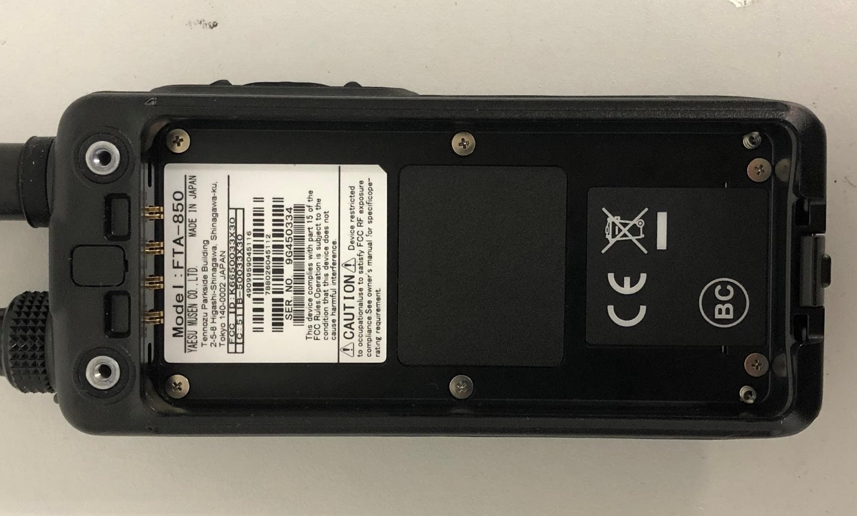
K6650033X30
Nov 18, 2020Airband Radio Transceiver
Equipment Class
TNF - Licensed Non-Broadcast Transmitter Held to Face