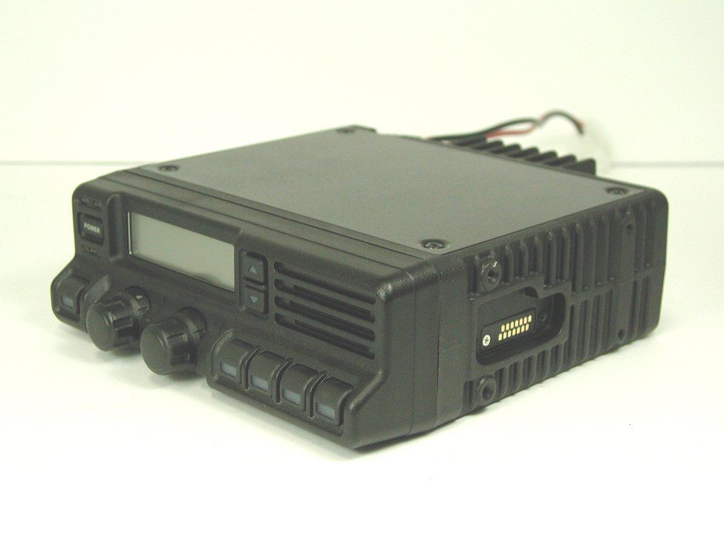
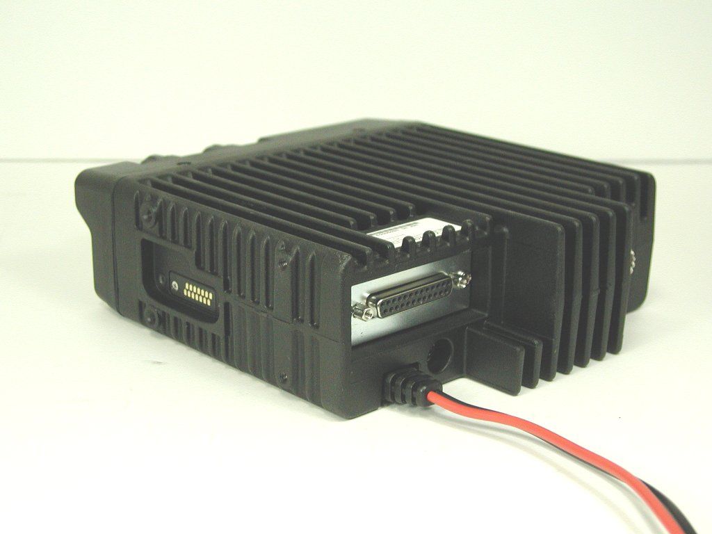
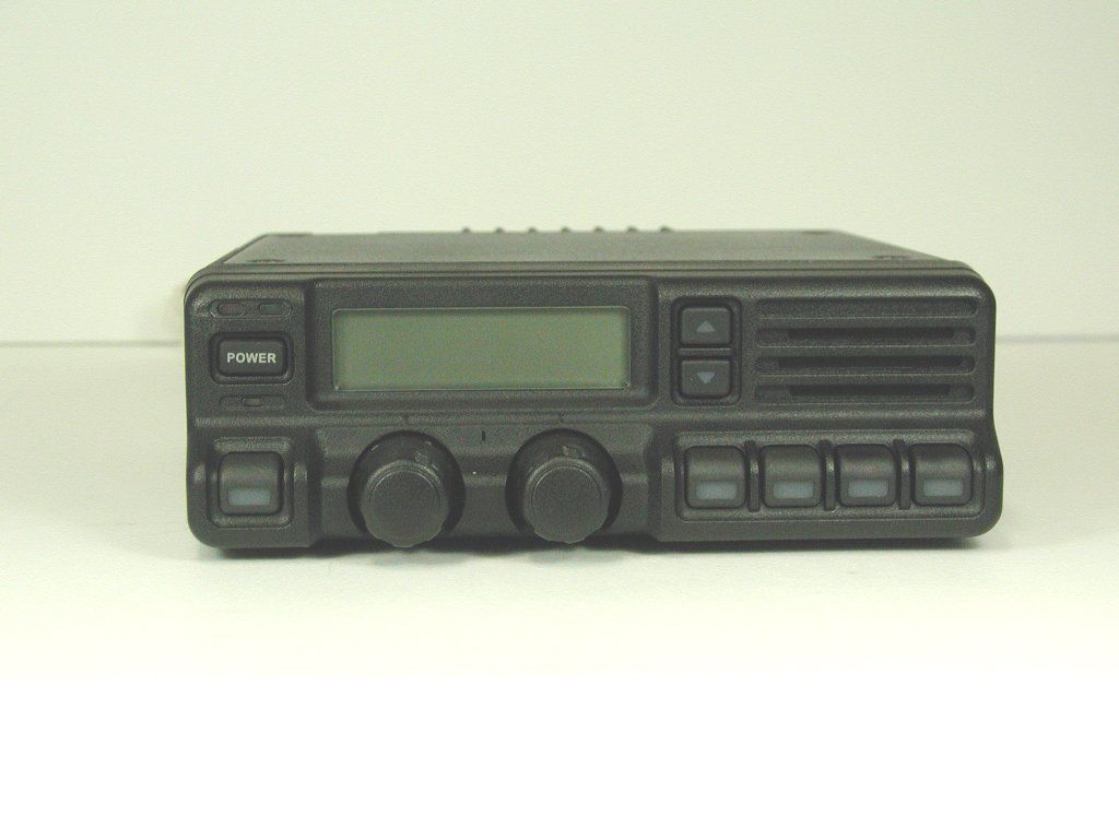
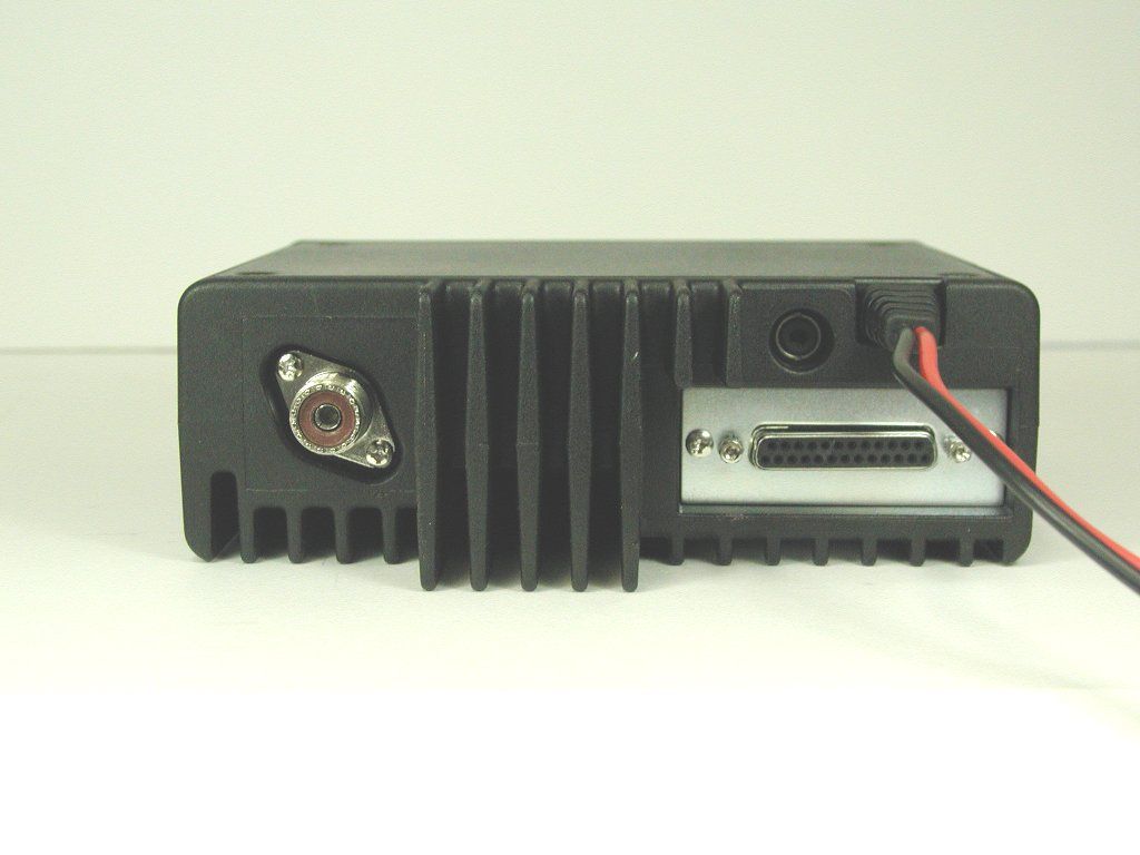
K66VX-4000VENonbroadcast Transmitter (Mobile)
Yaesu Musen Co., Ltd.
Click to zoom
Application Details
- Equipment Class
- TNB - Licensed Non-Broadcast Station Transmitter
- Date of Grant
- Apr 18, 2001
- Application Purpose
- Original Equipment
- Date of Application
- Dec 25, 2000
- Equipment Note
- Nonbroadcast Transmitter (Mobile)
- Frequency Range
- 134.00000000 - 174.00000000
- Company
- Yaesu Musen Co., Ltd.
- Country
- Japan
Documents & Files
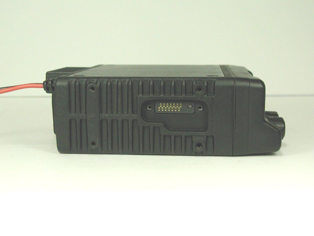
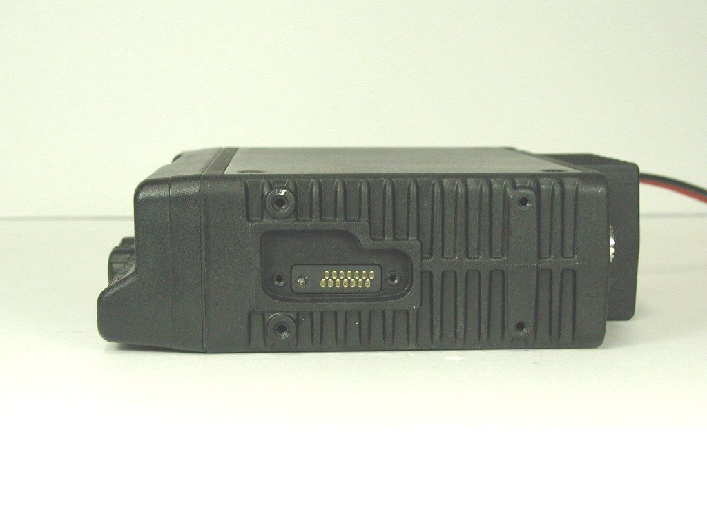
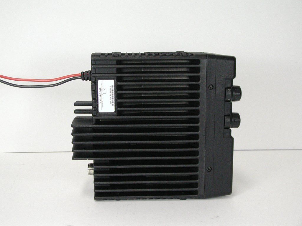
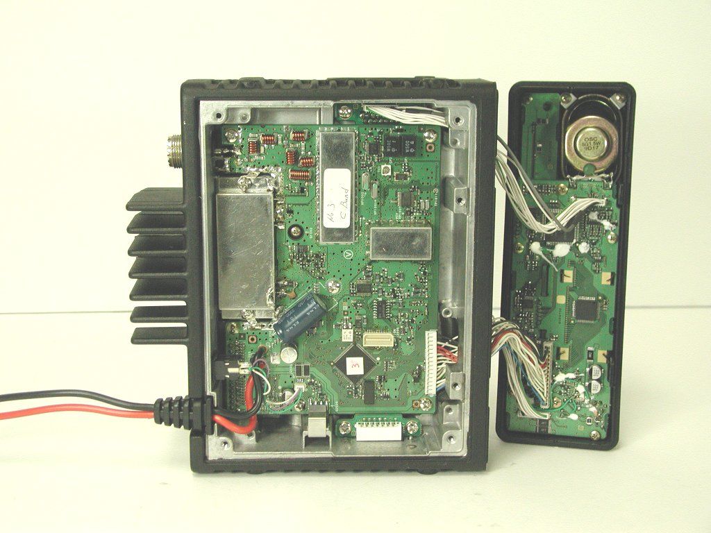
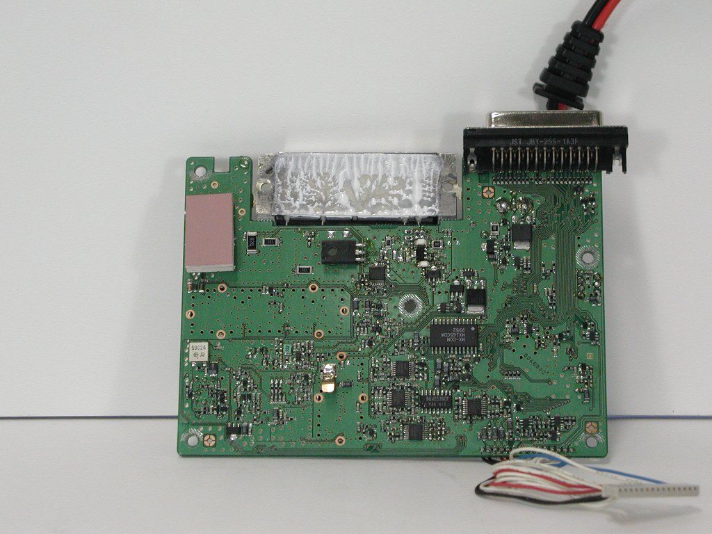
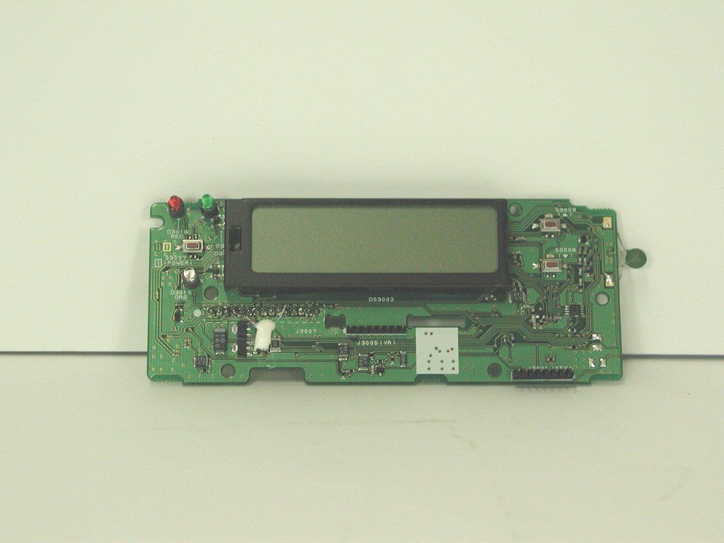
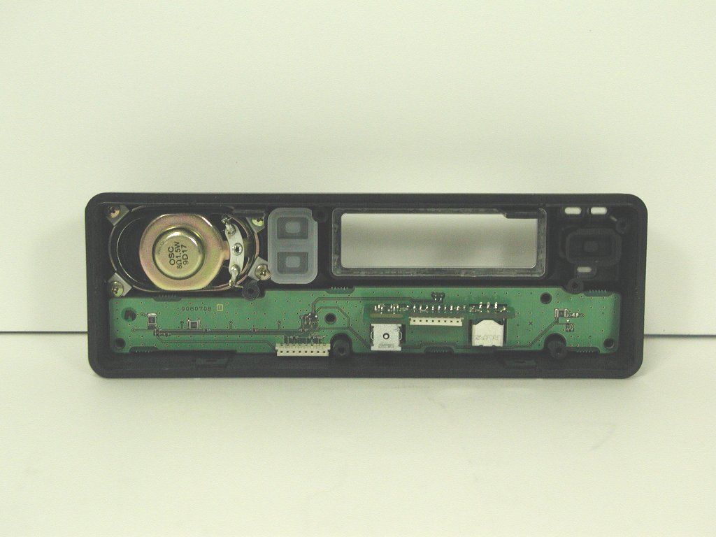
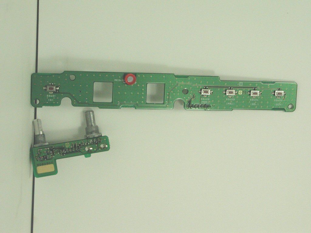
Document Text
Text extracted from the exhibit documents filed with the FCC. Open a document above to read the original.
Operational Description
Circuit Description Reception and transmission are switched by “RX” and ” TX” lines from the microprocessor unit (MPU). The receiver uses double-conversion superheterodyne circuitry, with a 43.95MHz 1st IF and 450 kHz 2nd IF. The 1st LO, produced by a PLL synthesizer, yields the 43.95MHz 1st IF. The 2nd LO uses a 43.5 MHz (43.95 MHz-450 kHz) signal generated by a crystal oscillator. The 2nd mixer and other circuits use a custom IC to convert and amplify the 2nd IF, and detect FM to obtain demodulated signals. During transmit, the PLL synthesizer oscillates at the desired frequency directly, for amplification to obtain RF power output. During transmit, voice modulation and CTCSS (or DCS) modulation are applied to this synthesizer. Transceiver functions, such as TX/RX control, PLL synthesizer settings, and channel programming, are controlled using the MPU. VHF Receive r Incoming RF signals from the antenna connector are delivered to the MAIN Unit, and pass through a low-pass filter (LPF) antenna switching network consisting of coils L1001, L1002, L1003 and L1006, capacitors C1001,C1006, C1009, C1013, and C1023, and antenna switching diodes D1006,D1007 and D1008 for delivery to the receiver front end. Signals within the frequency range of the transceiver are then passed through a varactor-tuned bandpass filter consisting of L1008, L1009 / L1024, L1025 before RF amplification by Q1012 (3SK228). The amplified RF is then band-pass filtered again by varactor-tuned resonators L1018, L1019 / L1038, L1039 to ensure pure in-band input to 1st mixer Q1025(2SK228). Buffered output from the VCO Unit is amplified by Q1021 (2SC5107) and low-pass filtered by L1042 / L1046 and C1132 / C1139 / C1142, to provide a pure 1st local signal between 112.3 and 152.3 MHz to the 1st mixer. The 43.95MHz 1st mixer product then passes through dual monolithic crystal filters XF1001 and XF1002 (7.5 kHz BW), and is amplified by Q1029 (2SC4215Y) and delivered to the input of the FM IF subsystem IC Q1026 (TA31136FN). This IC contains the 2nd mixer, 2nd local oscillator, limiter amplifier, FM detector, noise amplifier, and squelch gates. The 2nd LO in the IF-IC is produced from crystal X1001 (14.500MHz), and the 1st IF is converted to 450kHz by the 2nd mixer and stripped of unwanted components by ceramic filter CF1001 or CF1002. After passing through a limiter amplifier, the signal is demodulated by the FM detector. Demodulated receive audio from the IF-IC is amplified by Q1031 (2SA1602A) / Q2014 (CXA1846N). After volume adjustment by the AF power amplifier Q2029 (TDA7240AV), the audio signal is passed to the optional headphone jack or 4-ohm loudspeaker. PLL synthesizer The 1st LO maintains stability from the PLL synthesizer by using a 14.500 MHz reference signal from crystal X1001. PLL synthesizer IC Q1024 (SA7025DK) consists of a prescaler, reference counter, swallow counter, programmable counter, a serial data input port to set these counters based on the external data, a phase comparator, and charge pump. The PLL-IC divides the 14.500 MHz reference signal by 725 using the reference counter (20.0 kHz comparison frequency). The phase detector comparison frequency to be eight times the channel spacing (2.5kHz). The VCO output is divided by the prescaler, swallow counter and programmable counter. These two signals are compared by the phase comparator and input to the charge pump. A voltage proportional to their phase difference is delivered to the low-pass filter circuit, then fed back to the VCO as a voltage with phase error, controlling and stabilizing the oscillating frequency. This synthesizer also operates as a modulator during transmit. The RX-VCO is comprised of Q1015 (2SK520) and D1017, D1018, D1035, D1036 (HVU356x4), and oscillates between 177.950MHz and 217.950MHz according to the programmed receiving frequency. And the TX-VCO is comprised of Q1014 (2SC5107) and D1015, D1016, D1019 (1SV276x3), and oscillates between 134.000MHz and 174.000MHz according to the programmed transmit frequency. The VCO output passes through buffer amplifier Q1018 (2SC5107), and a portion is fed to the buffer amplifier Q1019 (2SC5107) of the PLL IC, and at the same time amplified by Q1021 (2SC5107) to obtain stable output. The VCO DC supply is regulated by Q1008 (2SC4154E). Synthesizer output is fed to the 1st mixer by diode switch D1024 (1SS321) during receive, and to drive amplifier Q1020/Q1022 (2SC5415Ex2) for transmit. The reference oscillator feeds the PLL synthesizer, and is composed of crystal X1001 (14.500 MHz), the temperature compensation circuit which includes D1033 (MC2850) and thermostats TH1003 and TH1002, and transmit (DCS) modulation circuit D1029 (1SV2309). Transmitter Voice audio from the microphone is delivered via the Mic (Jack) Unit to the MAIN Unit, after passing through amplifier Q3039/Q2108 (NJM2902V), pre-emphasis, limiter (IDC instantaneous deviation control) ,and LPF Q2001 (NJM2902V), is adjusted for optimum deviation level and delivered to the next stage. Voice input from the microphone and CTCSS are FM- modulated to the VCO of the synthesizer, while DCS audio is modulated by the reference frequency oscillator of the synthesizer. Synthesizer output, after passing through diode switch D1024 (1SS321), is amplified by driver Q1020 / Q1022 (2SC5415Ex2) and power module Q1013 (M67746) to obtain full RF output. The RF energy then passes through antenna switch D1007 / D1008 and a low-pass filter circuit and finally to the antenna connector. RF output power from the final amplifier is sampled by CM coupler and is rectified by D1011, D1014 (HSM88ASx2). The resulting DC is fed through Automatic Power Controller Q1007 (NJM2904V), Q1001 (2SC4154E), Q1002 (2SB1143S) to transmitter RF amplifier and thus the power output. Generation of spurious products by the transmitter is minimized by the fundamental carrier frequency being equal to the final transmitting frequency, modulated directly in the transmit VCO. Additional harmoni…
Text truncated - open the document above for the full version.
Parts List/Tune Up Info
Alignment The VX-4000 has been carefully aligned at the factory for the specified performance across the frequency range specified for each version. Realignment should therefore not be necessary except in the event of a component failure, or alteration of version. All component replacement and service should be performed only by an authorized Yaesu representative, or the warranty policy may be voided. The following procedures cover the sometimes critical and tedious adjustments that are not normally required once the transceiver has left the factory. However, if damage occurs and some parts are replaced, realignment may be required. If a sudden problem occurs during normal operation, it is likely due to component failure; realignment should not be done until after the faulty component has been replaced. We recommend that servicing be performed only by authorized Yaesu service technicians who are experienced with the circuitry and fully equipped for repair and alignment. Therefore, if a fault is suspected, contact the dealer from whom the transceiver was purchased for instructions regarding repair. Authorized Yaesu service technicians realign all circuits and make complete performance checks to ensure compliance with factory specifications after replacing any faulty components. Those who do undertake any of the following alignments are cautioned to proceed at their own risk. Problems caused by unauthorized attempts at realignment are not covered by the warranty policy. Also, Yaesu must reserve the right to change circuits and alignment procedures in the interest of improved performance, without notifying owners. Under no circumstances should any alignment be attempted unless the normal function and operation of the transceiver are clearly understood, the cause of the malfunction has been clearly pinpointed and any faulty components replaced, and the need for realignment determined to be absolutely necessary. The following test equipment (and thorough familiarity with its correct use) is necessary for complete realignment. Correction of problems caused by misalignment resulting from use of improper test equipment is not covered under the warranty policy. While most steps do not require all of the equipment listed, the interactions of some adjustments may require that more complex adjustments be performed afterwards. Do not attempt to perform only a single step unless it is clearly isolated electrically from all other steps. Have all test equipment ready before beginning, and follow all of the steps in a section in the order presented. Required Test Equipment RF signal generator: calibrated output level at 1000 MHz (0 dBμ =1.0 μV - closed circuit) Deviation Meter (linear detector) AF Millivoltmeter SINAD Meter Inline Wattmeter with 5% accuracy at 1000 MHz Regulated DC Power Supply: adjustable from 10 to 17 VDC, 15A 50-ohm Non-reactive Dummy Load: 100W at 1000 MHz Frequency Counter: >0.1 ppm accuracy at 1000 MHz AF Signal Generator DC Voltmeter: high impedance RF Sampling Coupler(attenuation pad) AF Dummy Load: 4 ohm, 20W Oscilloscope Spectrum Analyzer IBM PC/compatible computer w/Yaesu CT-71 programming cable and CE-35 channel programming editor. 50-ohms RF Signal Dummy load Generator RF Sampling Inline Wattmeter Coupler Transceiver Deviation Meter CT-70 CT-29 Connection Frequency Cable Power Supply Counter IBM PC 13.8V DC COM port Alignment Preparation & Precautions A dummy load and inline wattmeter must be connected to the main antenna jack in all procedures that call for transmission, except where specified otherwise. Correct alignment is not possible with an antenna. After completing one step, read the following step to determine whether the same test equipment will be required. If not, remove the test equipment (except dummy load and wattmeter, if connected) before proceeding. Correct alignment requires that the ambient temperature be the same as that of the transceiver and test equipment, and that this temperature be held constant between 20 and 30°C (68 86F). When the transceiver is brought into the shop from hot or cold air it should be allowed some time for thermal equalization with the environment before alignment. If possible, alignments should be made with oscillator shields and circuit boards firmly affixed in place. Also, the test equipment must be thoroughly warmed up before beginning. Before beginning, connect the transceiver and PC using the CT-71 programming cable as described in the EEPROM Programming chapter, and download the EEPROM data from the transceiver to the computer. Store this data in a disk file so that it can be saved and retrieved later. Using the table below, program the channel, CTCSS, and DCS alignment settings for your transceiver version. Upload this file to the transceiver. Note: Signal levels in dB referred to in this procedure are based on 0 dBm = 0.5 mV (closed circuit). Caution: Do not connect this line to ground, and be certain that the speaker has adequate capability to handle the audio output from the radio. Because of the bridge audio amplifier circuit used in the radio, it is necessary to construct and use a simple audio load test adapter as shown in the schematic diagram above, when conducting receiver alignment steps. 3.5mm PLUG Attenuated Test Output(1/2) 2ohms 10W Ground + 470uF 2ohms 10W AF Test Adapter Schematic Alignment Channel Frequencies VHF TYPE A ChannelFrequency (simplex) CTCSS Encode DCS Encode Narrow /wide CH1134.01MHzNoneNoneWide CH2147.01MHzNoneNoneWide CH3159.99MHzNoneNoneWide CH4134.01MHzNoneNoneNarrow CH5147.01MHzNoneNoneNarrow CH6159.99MHzNoneNoneNarrow CH7147.01MHz151.4HzNoneWide CH8147.01MHzNone023Wide CH9147.01MHz151.4HzNoneNarrow CH10147.01MHzNone023Narrow VHF TYPE C ChannelFrequency (simplex) CTCSS Encode DCS Encode Narrow /wide CH1148.01MHzNoneNoneWide CH2161.01MHzNoneNoneWide CH3173.99MHzNoneNoneWide CH4148.01MHzNoneNoneNarrow CH5161.01MHzNoneNoneNarrow CH6173.99MHzNoneNoneNarrow CH7161.01MHz151.4HzNoneWide CH8161.01…
Text truncated - open the document above for the full version.
Parts List/Tune Up Info
VX-4000 Component Application..xls, 1/3 AddressDevice nameDescriptionApplication [MAIN] Q 1001Transistor2SC4154ETx Po Control Q 1002Transistor2SB1143STx Po Control Q 1003Transistor2SB1201STPVoltage Suppl Control Q 1004TransistorRT1N241MTx Po Control Q 1005TransistorDTB123EKRx 9V Switch Q 1006Transistor2SB1132RTx 9V Switch Q 1007ICNJM2904VBPF Tune Buff/APC COMP Q 1008Transistor2SC4154E9V Regulator Q 1009TransistorIMH6Tx/Rx Switch Q 1010Not Used Q 1011TransistorRT1N241MMic Mute Q 1012Transistor3SK228XRRF Amplifier Q 1013ICM67746-1RF PWR-MODULE Q 1014Transistor2SC5107-Ovoltage Control Oscillator Q 1015Transistor2SK520voltage Control Oscillator Q 1016TransistorRT1N241MTx/Rx Switch Q 1017TransistorIMH6Tx/Rx Switch Q 1018Transistor2SC5107-OBuff AMP Q 1019Transistor2SC5107-OBuff AMP Q 1020Transistor2SC5415ETx Driver AMP Q 1021Transistor2SC5107-OBuff AMP Q 1022Transistor2SC5415ETx Driver AMP Q 1023ICNJM78L05UA5V Regulator Q 1024ICSA7025DKPLL Subsystem Q 1025Transistor3SK228XRRx MIX Q 1026ICTA31136FNIF Subusystem Q 1027Transistor2SC4154EReference Oscillator Q 1028TransistorRT1N241MRx Wide/Narrow Switch Q 1029Transistor2SC4215YIF Buff AMP Q 1030ICMM1216ENRE9V Regulator Q 1031Transistor2SA1602AAF Buff AMP Q 1032TransistorRT1N241MAF Wide/Narrow Switch Q 1033TransistorRT1N241MRF Gain Control Q 2001ICNJM2902VEnphasis/IDC/LPF/MIX Q 2002TransistorIMZ1Line Buff Q 2003ICNJM2902VRSSI/SQL/LPF Q 2004TransistorRT1N241MAnalog Switch Q 2005Not Used Q 2006TransistorRT1N241MAF Mute Q 2007ICBU4066BFAnalog Switch Q 2008TransistorRT1N241MMIC Mute Switch Q 2009TransistorIMX1Line Buff Q 2010Not Used Q 2011TransistorRT1N241MAF Mute Q 2012TransistorDTC323TKAF Mute Q 2013TransistorMX165CDWCTCSS Encoder/Decoder Q 2014ICCXA1846NAF VR Q 2015TransistorDTB123EKAnalog Switch Q 2016ICBU4053BCFAnalog Switch Q 2017Not Used Q 2018Transistor2SC4154EAnalog Switch Q 2019ICMB90F583BMicroproccesor Q 2020Transistor2SJ327-ZPower Supply Switch Q 2021Not Used Q 2022Not Used Q 2023Not Used Q 2024ICNJM78L05UA5V Regulator Q 2025Transistor2SA1602ACPU Reset Q 2026TransistorRT1N241MCPU Reset Q 2027ICS-80735SN-DZCPU Reset Q 2028ICHN58X2432TIProgrammable Data Stor Q 2029ICTDA7240AVAF AMP Q 2108ICNJM2902VAF AMP Q 2109Not Used Q 2110ICNJM2902VDCS Decder/AMP Q 2111TransistorDTB123EKAnalog Switch Q 2112TransistorIMD3Buff Q 2113Not Used Q 2114TransistorRT1N241MExternal SQL Switch Q 2115TransistorIMD3Buff Q 2116TransistorRT1N241MAnalog Switch Q 2117ICTC4W53FUAnalog Switch YAESU MUSEN CO., LTD. VX-4000 Component Application..xls, 2/3 AddressDevice nameDescriptionApplication Q 2118TransistorRT1N241MAF Mute Q 2119TransistorRT1N241MMic Mute Q 2120TransistorRT1N241MAnalog Switch Q 2121TransistorRT1N241MAnalog Switch Q 2122TransistorRT1N241MAnalog Switch Q 2123 Q 2124 Q 2125TransistorRT1N241MDCS Wide/Narrow Switch D 1001DiodeRLS135Antenna Switch D 1002DiodeBAS316Limiting Diode D 1003DiodeP6KA18Reverse Voltage Protecion D 1004Not Used D 1005DiodeBAS316Discharge D 1006DiodeUM9957FAntenna Switch D 1007DiodeUM9957FAntenna Switch D 1008DiodeUM9957FAntenna Switch D 1009Varactor Diode1SV229BPF Tune D 1010Varactor Diode1SV229BPF Tune D 1011DiodeHSM88ASPower Detect D 1012Varactor Diode1SV229BPF Tune D 1013Varactor Diode1SV229BPF Tune D 1014DiodeHSM88ASPower Detect D 1015Varactor DiodeHVU306AVCO D 1016Varactor DiodeHVU306AVCO D 1017Varactor DiodeHVU356VCO D 1018Varactor DiodeHVU356VCO D 1019Varactor Diode1SV276VCO D 1020Varactor Diode1SV229BPF Tune D 1021Varactor Diode1SV229BPF Tune D 1022Varactor Diode1SV229BPF Tune D 1023Varactor Diode1SV229BPF Tune D 1024Diode1SS321Tx/Rx RF Switch D 1025DiodeBAS316Discharge D 1026DiodeMC28482nd IF Filter Switich D 1027Diode02CZ5.6Y5V Supply D 1028DiodeMC28482nd IF Filter Switich D 1029Varactor Diode1SV230DCS MOD D 1030Varactor Diode1SV230Temp. Control for PLL REF D 1031Not Used D 1032Not Used D 1033DiodeMC2850Temp. Control for PLL REF D 1034DiodeBAS316APC D 1035Varactor DiodeHVU356VCO D 1036Varactor DiodeHVU356VCO D 2001DiodeMC2846External PTT D 2002DiodeMC2850DCS Decoder D 2003DiodeMC2850Noise Detector D 2004DiodeMC2850Noise Detector D 2005DiodeBAS316CTCSS Detector D 2006DiodeMC2850Limiting Diode D 2007DiodeMC2846Reverse Voltage Protecion D 2008Not Used D 2009Not Used D 2010DiodeMC2850Reverse Voltage Protecion D 2011DiodeBAS316Reverse Voltage Protecion D 2012DiodeBAS316Reverse Voltage Protecion D 2013DiodeBAS316Reverse Voltage Protecion D 2014DiodeBAS316Reverse Voltage Protecion D 2015DiodeBAS316Reverse Voltage Protecion [DISPLAY] Q 3001ICLC75823WLCD Driver Q 3002Not Used Q 3003TransistorRT1N241MMic Mute Q 3004TransistorIMZ1 Line Buff Q 3005TransistorRT1N241MDATA Line Mute Q 3006Not Used Q 3007TransistorIMD3Buff Q 3008TransistorRT1N241MMic Mute Q 3009TransistorRT1N241MMic Mute Q 3010TransistorIMX1Line Buff YAESU MUSEN CO., LTD. VX-4000 Component Application..xls, 3/3 AddressDevice nameDescriptionApplication Q 3011TransistorIMZ1 Buff Q 3012ICS-93C46AMFNProgrammable Data Stor Q 3013TransistorIMD3Buff Q 3014ICHD64F3642AHCPU Q 3015TransistorIMH6ASwitich for flash mode Q 3016ICS-80735SNCPU Reset Q 3017Transistor2SA1602APower Down Detect Q 3018Not Used Q 3019Transistor2SC4154Xtal Shift Switch Q 3020TransistorRT1N241MAF MUTE Q 3021ICNJM78L05UA5V Regulator Q 3022TransistorRT1N241MSwitich for flash mode Q 3023Not Used Q 3024TransistorRT1N241MPanel Interface Detect Q 3025TransistorRT1N241MVolume Control ON/OFF Q 3026TransistorRT1N241MPower Switch Control Q 3027TransistorPower Switch ControlPower Down Detect Q 3028Transistor2SB1132Power Switch Q 3029Transistor2SB1132LED DRIVER Q 3030TransistorUMW1NBrightness Control Q 3031Transistor2SB1132Power Switch Q 3032Not Used Q 3033TransistorIMH6APower Switch Control Q 3034Not Used Q 3035Not Used Q 3036Not Used Q 3037Not Used Q 3038TransistorIMX1AGC AMP Q 3039ICNJM2902VMIC AMP Q 3040TransistorIMZ1 BUFF Q 3041Not Used Q 3042Not Used Q 3043ICTC4S66FAnalog Switch D 3001Not Used D 3002Not Used D 3003Not Used D 3004Not Used D 3005Diode1SS226AGC rectification D 3006DiodeDAP202U FLASH CPU Writing D 3007Not Us…
Text truncated - open the document above for the full version.
RF Exposure Info
FCC ID: K66VX-4000VE MFA p0070015, d00c0029 ENVIRONMENTAL ASSESSMENT for MOBILES for FCC ID: FCC ID: K66VX-4000VE Model:VX-4000V Type A and C to FEDERAL COMMUNICATIONS COMMISSION 47 CFR 1.1310 (MPE) Radiofrequency Radiation Exposure Limits DATE OF REPORT: December 22, 2000 ON THE BEHALF OF THE APPLICANT: Vertex Standard Co., Ltd. AT THE REQUEST OF: P.O. Email of 12/20/2000 Vertex Standard USA Inc. 17210 Edwards Rd. Cerritos, CA 90703 Attention of: Mikio Maruya, Executive Vice President (800) 255-9237; FAX: (800) 477-9237 (562) 404-2700, x280; FAX: -1210 [email protected] SUPERVISED BY: Morton Flom, P. Eng. FCC ID: K66VX-4000VE MFA p0070015, d00c0029 TABLE OF CONTENTS RULEDESCRIPTIONPAGE . Test Report 1 . Identification of the Equipment Under Test 2 . Standard Test Conditions and Engineering Practices 4 1.1310 Environmental Assessment 5 FCC ID: K66VX-4000VE MFA p0070015, d00c0029 PAGE NO.1of8. Required information per ISO/IEC Guide 25-1990, paragraph 13.2: a) TEST REPORT (SUPPLEMENTAL) b) Laboratory: (FCC: 31040/SIT) (Canada: IC 2044) M. Flom Associates, Inc. 3356 N. San Marcos Place, Suite 107 Chandler, AZ 85225 c) Report Number: d00c0029 d) Client: Vertex Standard USA Inc. 17210 Edwards Rd. Cerritos, CA 90703 e) Identification: VX-4000V and VX-4000VA FCC ID: K66VX-4000VE Description: VHF FM Mobile Transceiver f) EUT Condition: Not required unless specified in individual tests. g) Report Date: December 22, 2000 EUT Received: July 20, 2000 h, j, k): As indicated in individual tests. i) Sampling method: No sampling procedure used. l) Uncertainty: In accordance with MFA internal quality manual. m) Supervised by: Morton Flom, P. Eng. n) Results: The results presented in this report relate only to the item tested. o) Reproduction: This report must not be reproduced, except in full, without written permission from this laboratory. FCC ID: K66VX-4000VE MFA p0070015, d00c0029 PAGE NO.2of8. IDENTIFICATION OF THE EQUIPMENT UNDER TEST (EUT) NAME AND ADDRESS OF APPLICANT: Vertex Standard Co., Ltd. 4-8-8 Nakameguro, Meguro-Ku Tokyo 153-8644 Japan MANUFACTURER: Applicant FCC ID: K66VX-4000VE MODEL NO: VX-4000V Type A (136-160 MHz) VX-4000V Type C (148-174 MHz) DESCRIPTION: VHF FM Mobile Transceiver TYPE OF EMISSION: 16K0F3E, 11K0F3E FREQUENCY RANGE, MHz: 134 to 160, 148 to 174 POWER RATING, Watts: 5 to 50 Switchable x Variable N/A MODULATION: AMPS TDMA CDMA x F3E ANTENNA: HELICAL MONOPOLE WHIP x OTHER NOTE: For RF Safety test antenna gain taken at the upper range of expected gain (i.e. 0 dBd) and RF Power set to highest nominal power across all channels. FCC ID: K66VX-4000VE MFA p0070015, d00c0029 PAGE NO.3of8. M. Flom Associates, Inc. is accredited by the American Association for Laboratory Association (A2LA) as shown in the scope below. "This laboratory is accredited by the American Association for Laboratory Accreditation (A2LA) and the results shown in this report have been determined in accordance with the laboratory's terms of accreditation unless stated otherwise in the report." Should this report contain any data for tests for which we are not accredited, or which have been undertaken by a subcontractor that is not A2LA accredited, such data would not covered by this laboratory's A2LA accreditation. FCC ID: K66VX-4000VE MFA p0070015, d00c0029 PAGE NO.4of8. STANDARD TEST CONDITIONS and ENGINEERING PRACTICES Except as noted herein, the following conditions and procedures were observed during the testing: In accordance with ANSI C63.4-1992/2000, section 6.1.9, and unless otherwise indicated in the specific measurement results, the ambient temperature of the actual EUT was maintained within the range of 10°to 40°C (50°to 104°F) unless the particular equipment requirements specify testing over a different temperature range. Also, unless otherwise indicated, the humidity levels were in the range of 10% to 90% relative humidity. Prior to testing, the EUT was tuned up in accordance with the manufacturer's alignment procedures. All external gain controls were maintained at the position of maximum and/or optimum gain throughout the testing. Measurement results, unless otherwise noted, are worst case measurements. FCC ID: K66VX-4000VE MFA p0070015, d00c0029 PAGE NO.5of8. Name of test:Environmental Assessment Specification:FCC: 47 CFR 1.1310 Measurement Guide:ANSI/IEEE C95.1 1992 Test Equipment:Maximum Permissible Exposure (MPE) measurement system, consisting of: Narda 8717-1174R, Radiation meter Narda 8761D, E-field probe (300 kHz – 3 GHz) (Calibrated Nov-98) Measurement Procedure: 1. The following measurements were performed with a Narda probe using ANSI/IEEE C95.1 as a guide. 2. Prior to making any measurements, the measurements system was calibrated in accordance with the manufacturer’s procedures. 3. The EUT’s radiating element (antenna) was placed ona1mtall table for ease of testing. For equipment normally operated on a metal surface, a ground plane was used. 4. The remaining equipment necessary to operate the EUT was maintained at a distance from the measurement arrangement suitable to minimize interference with the measurements. 5. The minimum safe distance was calculated from the formula Power Density = EIRP / 4πR 2 (Peak Watts/m 2 ). The calculation is shown with the measurement data. 6. With the EUT operating at maximum power, a search was initiated for worst case emissions with the probe raised and lowered over a range of 0.2 to 2 meters in height and over a horizontal plane of 0 o to 360 o . 7. Average values were calculated for the whole body (0.2-2.0m), lower body (0.2-0.8m) and upper body (1.0-2.0m). Results: Attached. FCC ID: K66VX-4000VE MFA p0070015, d00c0029 PAGE NO.6of8. TEST SETUP: Maximum Permissible Exposure (MPE) g0070629: 2000-Jul-25 Tue 15:11:10 STATE: 0:General TEST SETUP: Maximum Permissible Exposure (MPE) g0070630: 2000-Jul-25 Tue 15:11:10 STATE: 0:General FCC ID: K66VX-4000VE MFA p0070015, d00c0029 PAGE NO.7of8. TEST SETUP: Maximum Permissible Exposure (MPE) g0070695: 200…
Text truncated - open the document above for the full version.
Contact Information
Applicant
Masatoshi Muraishi(Engineering Division)
Technical Contact
M. Flom Associates, IncMorton Flom
[email protected]480 926 3100
3356 N. San Marcos Pl., Suite 107 · Chandler, Arizona · United States
Non-Technical Contact
M. Flom Associates, Inc.Morton Flom
[email protected]480 926 3100
Test Firm
M. Flom Associates, Inc.Morton Flom
Technical Specifications
| # | Rule Parts | Frequency Range | Power Output | Emission | Tolerance |
|---|---|---|---|---|---|
| 4 | 22,74,9 | 134 MHz - 174 MHz | 50 W | 16K0F3E | 2.5 ppm |
Other Applications from Yaesu Musen Co., Ltd.
K660E180X10
Dec 01, 2025BLUETOOTH MICROPHONE
Equipment Class
DTS - Digital Transmission System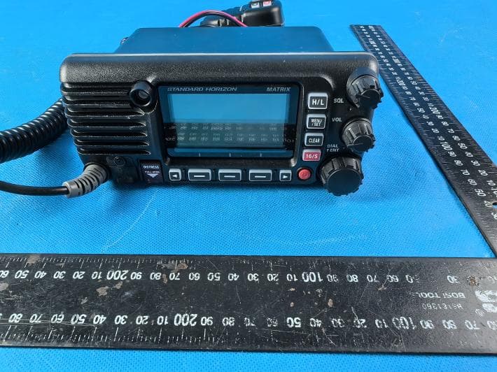
K6630673Y3D
Aug 01, 2024VHF FM Marine Transceiver
Equipment Class
CXX - Communications Rcvr for use w/ licensed Tx and CBs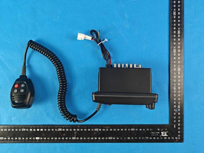
K6630653Y3D
Aug 01, 2024VHF FM Marine Transceiver
Equipment Class
CXX - Communications Rcvr for use w/ licensed Tx and CBs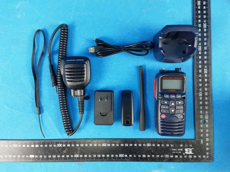
K6630683X30
Jan 10, 2023VHF FM Marine Transceiver
Equipment Class
TNF - Licensed Non-Broadcast Transmitter Held to Face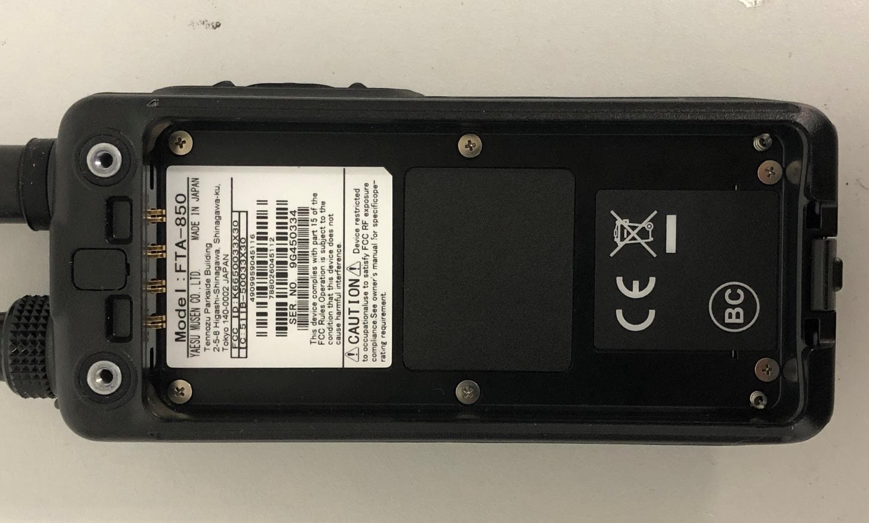
K6650033X30
Nov 18, 2020Airband Radio Transceiver
Equipment Class
TNF - Licensed Non-Broadcast Transmitter Held to Face