K66VX-5500V-2VHF Transceiver
Yaesu Musen Co., Ltd.
Click to zoom
Application Details
- Equipment Class
- TNB - Licensed Non-Broadcast Station Transmitter
- Date of Grant
- May 22, 2003
- Application Purpose
- Original Equipment
- Date of Application
- May 22, 2003
- Equipment Note
- VHF Transceiver
- Frequency Range
- 134.00000000 - 160.00000000
- Company
- Yaesu Musen Co., Ltd.
- Country
- Japan
Documents & Files
Document Text
Text extracted from the exhibit documents filed with the FCC. Open a document above to read the original.
Users Manual
VX-5500 OPERATING MANUAL POWER VERTEX STANDARD CO., LTD. 4-8-8 Nakameguro, Meguro-Ku, Tokyo 153-8644, Japan VERTEX STANDARD US Headquarters 10900 Walker Street, Cypress, CA 90630, U.S.A. International Division 8350 N.W. 52nd Terrace, Suite 201, Miami, FL 33166, U.S.A. YAESU EUROPE B.V. P.O. Box 75525, 1118 ZN Schiphol, The Netherlands YAESU UK LTD. Unit 12, Sun Valley Business Park, Winnall Close Winchester, Hampshire, SO23 0LB, U.K. VERTEX STANDARD HK LTD. Unit 5, 20/F., Seaview Centre, 139-141 Hoi Bun Road, Kwun Tong, Kowloon, Hong Kong Congratulations! You now have at your fingertips a valuable communications tool - a two-way radio! Rugged, reliable and easy to use, your radio will keep you in constant touch with your colleagues for years to come, with negligible maintenance down time. Please take a few minutes to read this manual carefully. The information presented here will allow you to derive maximum performance from your radio. After reading it, keep the manual handy for quick reference, in case questions arise later on. We’re glad you joined the team. Call on us any time, because our business is communications. Let us help you get your message across. NOTICE There are no user-serviceable points inside this transceiver. All service jobs must be referred to your Authorized Service Center or Network Administrator. Safety / Warning Information WARNING - DO NOT operate the VX-5500V radio when someone (bystanders) outside the vehicle is within following range. Safety Training information: Antennas used for this transmitter must not exceed an antenna gain of 0 dBd. The radio must be used in vehicle-mount configurations with a maximum operating duty factor not exceeding 50%, in typical Push-to-Talk configurations. This radio is restricted to occupational use, work related operations only where the radio operator must have the knowledge to control the exposure conditions of its passengers and bystanders by maintaining the minimum separation distance of following range. Failure to observe these restrictions will result in exceeding the FCC RF exposure limits. Antenna Installation: For rear deck trunk installation, the antenna must be located at least the following range away from rear seat passengers and bystanders in order to comply with the FCC RF exposure requirements. For roof top installation, the antenna must be placed in the center of the roof. Radiated frequency and Distance VX-5500V (C) 1.97 Feet (0.6 m) Page 1 VX-5500 Operating Manual VX-5500 Operating Manual The VX-5500 Series are full-featured FM transceivers designed for flexible mobile and base station business communications in the VHF (50/10 Watts: programmable) Land Mobile Bands. Each model is designed for reliable business communications in a wide variety of applications, with a wide range of operating capability provided by its leading- edge design. The 250-channels memories can each be programmed with a 8-character channel name. Important channel frequency data is stored in EEPROM and flash memory on the CPU, and is easily programmable by dealers using a personal computer and the VERTEX STAN- DARD CT-71 Programming Cable and CE49 Software. The pages which follow will detail the many advanced features provided on the VX-5500 transceiver. After reading this manual, you may wish to consult with your Network Ad- ministrator regarding precise details of the configuration of this equipment for use in your application. POWER Page 2 VX-5500 Operating Manual CONTROLS & CONNECTORS Front Panel ¿ POWER Botton Press the button to turn the transceiver ON and OFF. ¡ TX Indicator This lamp glows red when the radio is transmitting. ¬ BUSY Indicator This lamp glows green when the channel is busy. √ Liquid Crystal Display The display include an 8-character alpha-numeric section showing channel and group names, status and identity information, and error messages. Additional indicators on the display show priority channel assignments and scan include / exclude selection. POWER ÉÇÑÖ á àâä Ü Å 8 Character Alpha-numeric Display Channel Group Number This channel on “INTERCOM” ListThis channel on “SELECTABLE TONE” List This channel on “SCAN” List Receiver Monitor This channel on “PUBLIC ADDRESS” or “SPEAKER” List This channel on “HORN ALERT” List This channel on “OPTION” List This channel on “AUX A/B/C” List Page 3 VX-5500 Operating Manual ƒ p/q Button Pressing these buttons changes the current group (and displayed group number or name). Holding this button for more than 1/2 second causes the function to repeat. ≈ SQC Indicator This lamp glows orange when incorrect position at the setting of CE49. ∆ Programmable Function Button (PF button) This button can be set up for special applications, such as high/low power selection, monitor, dimmer, talk-around, and call alert function, as determined by your network requirements and programmed by your VERTEX STANDARD dealer. « VOLUME Knob This knob sets the volume of the receiver. » EMERGENCY Microphone The emergency microphone is located behind this small slit. When the emergency feature is activated, this Microphone is enabled. ... CHANNEL Selector Knob This knob select the operating channel. Programmable Function Button (PF button) This button can be set up for special applications, such as high/low power selection, monitor, dimmer, talk-around, and call alert function, as determined by your network requirements and programmed by your VERTEX STANDARD dealer. Side Panel Microphone Jack (It is on both sides.) Connect the microphone plug to this jack. CONTROLS & CONNECTORS Microphone Jack Page 4 VX-5500 Operating Manual ÉÇÅ Ñ REAR (Heatsink) ¿ Antenna Socket The 50-ohm coaxial feedline to the antenna must be connected here, using a type-M (PL-259) plug. ¡ External Speaker Jack An external loudspeaker may be connected to this 2-contact, 3.5-mm mini-phone jack. Caution: Do not connect this line to ground, and be certain that the speaker has adequate capability to handle the audio output from the VX-5500. …
Text truncated - open the document above for the full version.
External Photos
FCC ID: K66VX-5500V-2 Vertex Standard Co., Ltd. Front view Rear view FCC ID: K66VX-5500V-2 Vertex Standard Co., Ltd. Left view Right view FCC ID: K66VX-5500V-2 Vertex Standard Co., Ltd. Top view Bottom view FCC ID: K66VX-5500V-2 Vertex Standard Co., Ltd. Microphone DC Power Cable
ID Label/Location Info
VX-5500V-2VX-5500V-2 LABEL DRAWINGLABEL DRAWING Vertex Standard Co., Ltd.Vertex Standard Co., Ltd. (1:1) (1:2) ID / Part 15.19 and CAUTION drawings ID drawing Part 15.19 and CAUTION drawings This device complies with part 15 of FCC Rules. Operation is subject to the condition that this device does not cause harmful interference. Device restricted to occupational use to satisfy FCC RF exposure compliance. See owner’s manual for specific operating requirement. Label location CAUTION This device complies with part 15 of FCC Rules. Operation is subject to the condition that this device does not cause harmful interference. Device restricted to occupational use to satisfy FCC RF exposure compliance. See owner’s manual for specific operating requirement. CAUTION VX-5500V K66VX-5500V-2 -2 511B-VX5500V2 VERTEX STANDARD CO., LTD. MADE IN JAPAN 4909959000000 SER NO. 00000000 FCC ID: IC: VX-5500V K66VX-5500V-2 -2 511B-VX5500V2 VERTEX STANDARD CO., LTD. MADE IN JAPAN 4909959000000 SER NO. 00000000 FCC ID: IC:
Internal Photos
FCC ID: K66VX-5500V-2 Vertex Standard Co., Ltd. Inside of EUT Side-A of MAIN-UNIT with shield cases FCC ID: K66VX-5500V-2 Vertex Standard Co., Ltd. Side-A of MAIN-UNIT without shield cases Side-B of MAIN-UNIT FCC ID: K66VX-5500V-2 Vertex Standard Co., Ltd. Side-A of DISPLAY-UNIT with LCD Side-A of DISPLAY-UNIT without LCD FCC ID: K66VX-5500V-2 Vertex Standard Co., Ltd. Side-B of DISPLAY-UNIT Front of LCD FCC ID: K66VX-5500V-2 Vertex Standard Co., Ltd. Back of LCD Side-A of KEY-UNIT FCC ID: K66VX-5500V-2 Vertex Standard Co., Ltd. Side-B of KEY-UNIT Side-A of VR-UNIT FCC ID: K66VX-5500V-2 Vertex Standard Co., Ltd. Side-B of VR-UNIT Side-A of MIC-CONN-UNIT FCC ID: K66VX-5500V-2 Vertex Standard Co., Ltd. Side-B of MIC-CONN-UNIT Inside of front panel FCC ID: K66VX-5500V-2 Vertex Standard Co., Ltd. Inside of chassis Inside of microphone
Operational Description
FCC ID: K66VX-5500V-2 Circuit Description 1/3 Vertex Standard Co., Ltd. VX-5500V Circuit Description Reception and transmission are switched by “ RX ” and ” TX ” lines from the microprocessor unit (MPU). The receiver uses double-conversion super-heterodyne circuitry, with a 43.95MHz 1st IF and 450 kHz 2nd IF. The 1st LO, produced by a PLL synthesizer, yields the 43.95MHz 1st IF. The 2nd LO uses a 43.5 MHz (43.95 MHz-450 kHz) signal generated by a crystal oscillator. The 2nd mixer and other circuits use a custom IC to convert and amplify the 2nd IF, and detect FM to obtain demodulated signals. During transmit, the PLL synthesizer oscillates at the desired frequency directly, for amplification to obtain RF power output. During transmit, voice modulation and CTCSS (or DCS) modulation are applied to this synthesizer. Transceiver functions, such as Tx/Rx control, PLL synthesizer settings, and channel programming, are controlled using the MPU. Receiver Incoming RF signals from the antenna connector are delivered to the MAIN Unit, and pass through a low-pass filter (LPF) antenna switching network consisting of coils L2005, L2004, L2007 and L1003, capacitors C2219, C2218, C2217, C2216, and C1037, and antenna switching diodes D2015, D2016 and D2017 for delivery to the receiver front end. Signals within the frequency range of the transceiver are then passed through a varactor-tuned band-pass filter consisting of L1007, L1020 before RF amplification by Q1018 (2SC3357). The amplified RF is then band-pass filtered again by varactor-tuned resonators L1009, L1011 to ensure pure in-band input to 1st mixer Q1188, Q1189, Q1190, Q1191 (2SK520 × 4). Buffered output from the VCO Unit is amplified by Q1032 (2SC5107), Q1192 (2SC3357) and low-pass filtered by L1041 / L1045/ L1060and C1153 / C1154 / C1174/C1089, to provide a pure 1st local signal between 177.95 and 217.95 MHz to the 1st mixer. The 43.95MHz 1st mixer product then passes through dual monolithic crystal filters XF1001 and XF1002 (12 kHz BW)/ XF1003 and XF1004 (7kHz BW) and is amplified by Q1041 (2SC4215Y) and delivered to the input of the FM IF subsystem IC Q1034 (TA31136FN). This IC contains the 2nd mixer, 2nd local oscillator, limiter amplifier, FM detector, noise amplifier, and squelch gates. The 2nd LO in the IF-IC is produced from crystal OSC X1001 (14.500MHz), and the 1st IF is converted to 450kHz by the 2nd mixer and stripped of unwanted components by ceramic filter CF1001 or CF1002. After passing through a limiter amplifier, the signal is demodulated by the FM detector. Demodulated receive audio from the IF-IC is amplified by Q2019 (CXA1846N). After volume adjustment by the AF power amplifier Q2018 (TDA7240AV), the audio signal is passed to the optional headphone jack or 4 Ω loudspeaker. FCC ID: K66VX-5500V-2 Circuit Description 2/3 Vertex Standard Co., Ltd. PLL synthesizer The 1st LO maintains stability from the PLL synthesizer by using a 14.500 MHz reference signal from crystal OSC X1001. PLL synthesizer IC Q1033 (SA7025DK) consists of a prescaler, reference counter, swallow counter, programmable counter, a serial data input port to set these counters based on the external data, a phase comparator, and charge pump. The PLL-IC divides the 14.500 MHz reference signal by 725 using the reference counter (20.0 kHz comparison frequency). The phase detector comparison frequency to be eight times the channel spacing (2.5kHz). The VCO output is divided by the prescaler, swallow counter and programmable counter. These two signals are compared by the phase comparator and input to the charge pump. A voltage proportional to their phase difference is delivered to the low-pass filter circuit, then fed back to the VCO as a voltage with phase error, controlling and stabilizing the oscillating frequency. This synthesizer also operates as a modulator during transmit. The RX-VCO is comprised of Q1019 (2SK520) and D1010, D1011, D1016, D1018 (HVC306 x 4), and oscillates between 177.950MHz and 217.950MHz according to the programmed receiving frequency. And the TX-VCO is comprised of Q1020 (2SC5107) and D1014, D1015 (HVC306 x 2), D1020 (1SV284) and oscillates between 134.000MHz and 174.000MHz according to the programmed transmit frequency. The VCO output passes through buffer amplifier Q1026 (2SC5107), and a portion is fed to the buffer amplifier Q1029 (2SC5107) of the PLL IC, and at the same time amplified by Q1032 (2SC5107) to obtain stable output. The VCO DC supply is regulated by Q1006 (2SC4154E). Synthesizer output is fed to the 1st mixer by diode switch D1021 (1SS321) during receive, and to drive amplifier Q1031 (2SC3356) / Q1025 (2SC3357) for transmit. Transmitter Voice audio from the microphone is delivered via the MIC (Jack) Unit to the MAIN Unit, after passing through amplifier Q3039/Q2040 (NJM2902V), pre-emphasis, limiter (IDC instantaneous deviation control), and LPF Q2001 (NJM2902V), is adjusted for optimum deviation level and delivered to the next stage. Voice input from the microphone and CTCSS are FM-modulated to the VCO of the synthesizer, while DCS audio is modulated by the reference frequency oscillator of the synthesizer. Synthesizer output, after passing through diode switch D1025 (1SS321), is amplified by driver Q1031 (2SC3356) / Q1025 (2SC3357) and power module Q1017 (RA60H1317M) to obtain full RF output. The RF energy then passes through antenna switch D2015 / D2016 and a low-pass filter circuit and finally to the antenna connector. RF output power from the final amplifier is sampled by CM coupler and is rectified by D1037, D1038 (1SS400 x 2). The resulting DC is fed through Automatic Power Controller Q1007 (NJM2904V) to transmitter RF amplifier and thus the power output. Generation of spurious products by the transmitter is minimized by the fundamental carrier frequency being equal to the final transmitting frequency, modulated directly in the transmit VCO. Additional harmonic suppression is provided by a low-pass filter consisting of L2…
Text truncated - open the document above for the full version.
Parts List/Tune Up Info
FCC ID: K66VX-5500V-2 Alignment 1/4 Vertex Standard Co., Ltd. VX-5500V Alignment The VX-5500 has been carefully aligned at the factory for the specified performance across the frequency range specified for each version. Realignment should therefore not be necessary except in the event of a component failure, or alteration of version. All component replacement and service should be performed only by an authorized VERTEX STANDSRD representative, or the warranty policy may be voided. The following procedures cover the sometimes critical and tedious adjustments that are not normally required once the transceiver has left the factory. However, if damage occurs and some parts are replaced, realignment may be required. If a sudden problem occurs during normal operation, it is likely due to component failure; realignment should not be done until after the faulty component has been replaced. We recommend that servicing be performed only by authorized VERTEX STANDARD service technicians who are experienced with the circuitry and fully equipped for repair and alignment. Therefore, if a fault is suspected, contact the dealer from whom the transceiver was purchased for instructions regarding repair. Authorized VERTEX STANDARD service technicians realign all circuits and make complete performance checks to ensure compliance with factory specifications after replacing any faulty components. Those who do undertake any of the following alignments are cautioned to proceed at their own risk. Problems caused by unauthorized attempts at realignment are not covered by the warranty policy. Also, VERTEX STANDARD must reserve the right to change circuits and alignment procedures in the interest of improved performance, without notifying owners. Under no circumstances should any alignment be attempted unless the normal function and operation of the transceiver are clearly understood, the cause of the malfunction has been clearly pinpointed and any faulty components replaced, and the need for realignment determined to be absolutely necessary. The following test equipment (and thorough familiarity with its correct use) is necessary for complete realignment. Correction of problems caused by misalignment resulting from use of improper test equipment is not covered under the warranty policy. While most steps do not require all of the equipment listed, the interactions of some adjustments may require that more complex adjustments be performed afterwards. Do not attempt to perform only a single step unless it is clearly isolated electrically from all other steps. Have all test equipment ready before beginning, and follow all of the steps in a section in the order presented. Required Test Equipment RF signal generator: calibrated output level at 1000 MHz (0 dBμ =1.0 μV - closed circuit) Deviation Meter (linear detector) AF Millivoltmeter SINAD Meter Inline Wattmeter with 5% accuracy at 1000 MHz Regulated DC Power Supply: adjustable from 10 to 17 VDC, 15A 50 Ω Non-reactive Dummy Load: 100W at 1000 MHz Frequency Counter: >0.1-ppm accuracy at 1000 MHz AF Signal Generator DC Voltmeter: high impedance RF Sampling Coupler (attenuation pad) AF Dummy Load: 4 Ω , 20W Oscilloscope Spectrum Analyzer IBM PC/compatible computer w/ VERTEX STANDARD CT-71 programming cable and CE-35 channel programming editor. FCC ID: K66VX-5500V-2 Alignment 2/4 Vertex Standard Co., Ltd. 50-Ω RF Signal Dummy load Generator RF Sampling Inline Wattmater Coupler Transceiver Deviation Meter CT-70 CT-29 Connection Frequeuncy Cable Power Supply Counter IBM PC 13.8V DC COM port Alignment Preparation & Precautions A dummy load and inline wattmeter must be connected to the main antenna jack in all procedures that call for transmission, except where specified otherwise. Correct alignment is not possible with an antenna. After completing one step, read the following step to determine whether the same test equipment will be required. If not, remove the test equipment (except dummy load and wattmeter, if connected) before proceeding. Correct alignment requires that the ambient temperature be the same as that of the transceiver and test equipment, and that this temperature be held constant between 20 and 30 °C (68 and 86 °F). When the transceiver is brought into the shop from hot or cold air it should be allowed some time for thermal equalization with the environment before alignment. If possible, alignments should be made with oscillator shields and circuit boards firmly affixed in place. Also, the test equipment must be thoroughly warmed up before beginning. Before beginning, connect the transceiver and PC using the CT-71 programming cable as described in the EEPROM Programming chapter, and downloads the EEPROM data from the transceiver to the computer. Store this data in a disk file so that it can be saved and retrieved later. Using the table below, program the channel, CTCSS, and DCS alignment settings for your transceiver version. Upload this file to the transceiver. Note: Signal levels in dB referred to in this procedure are based on 0 dBm = 0.5 μV (closed circuit). Caution: Do not connect this line to ground, and be certain that the speaker has adequate capability to handle the audio output from the radio. Because of the bridge audio amplifier circuit used in the radio, it is necessary to construct and use a simple audio load test adapter as shown in the schematic diagram above, when conducting receiver alignment steps. 3.5 φ PLUG Attenuated Test Output (1/2) 2 Ω 10 W Ground + 470 μF 2 Ω 10 W AF Test Adapter Schematic FCC ID: K66VX-5500V-2 Alignment 3/4 Vertex Standard Co., Ltd. Alignment Channel Frequencies ChannelFrequency (simplex) CTCSS Encode DCS Encode Narrow /wide CH1134.01MHzNoneNoneWide CH2147.01MHzNoneNoneWide CH3159.99MHzNoneNoneWide CH4134.01MHzNoneNoneNarrow CH5147.01MHzNoneNoneNarrow CH6159.99MHzNoneNoneNarrow CH7147.01MHz151.4HzNoneWide CH8147.01MHzNone023Wide CH9147.01MHz151.4HzNoneNarrow CH10147.01MHzNone023Narrow PLL & Transmitter Set up th…
Text truncated - open the document above for the full version.
Parts List/Tune Up Info
FCC ID: K66VX-5500V-2 Component Applications, 1/3 VX-5500V COMPONENT APPLICATIONS Address Device nameDescriptionApplication [MAIN-UNIT] Q 1003 TransistorIMH6ATx Switch Q 1004 ICMM1216ENRE9V Regulator Q 1005 Transistor2SB1201S-TL9V Regulator Q 1006 Transistor2SC4154EVCO Regulator Q 1007 ICNJM2902VBPF Tune Buff/APC COMP Q 1010 TransistorRT1N241MWide/Narrow Switch Q 1011 Transistor2SB1132Tx 9V Switch Q 1012 Transistor2SB1132Rx 9V Switch Q 1014 TransistorIMH6ATx/Rx Switch Q 1015 TransistorRT1N241MMOD Mute Switch Q 1017 ICRA60H1317MRF PWR-MODULE Q 1018 Transistor2SC3357-T2 RFRF Amplifier Q 1019 Transistor2SK520-T2B K41Rx Voltage Control Oscillator Q 1020 Transistor2SC5107-OTx Voltage Control Oscillator Q 1021 Transistor2SC4116GRPLL Filter Q 1022 Transistor2SC4116GRPLL Filter Q 1023 Transistor2SA1602APLL Filter Q 1024 Transistor2SK2035PLL Filter Q 1025 Transistor2SC3357-T2 RFTx Driver Amp Q 1026 Transistor2SC5107-OVCO Buff Amp Q 1027 TransistorRT1N241MVCO Tx/Rx Switch Q 1028 TransistorIMH6AVCO Tx/Rx Switch Q 1030 Transistor2SC3357-T2 RFIF Amp Q 1031 Transistor2SC3356-T2B R24Tx Driver Amp Q 1032 Transistor2SC5107-OBuff Amp Q 1033 ICSA7025DKPLL IC Q 1034 ICTA31136FN2nd IF IC Q 1035 Transistor2SC4154EReference Oscillator Buff Amp Q 1038 ICNJM78L05UAPLL 5V Regulator Q 1041 Transistor2SC4215YIF AMP Q 1042 TransistorRT1N241MWide/Narrow Switch Q 1044 TransistorRT1N241MWide/Narrow Switch Q 1045 TransistorIMH6AWide/Narrow Switch Q 1046 ICRN5RL30AA-TRReference Oscillator 3V Regulator Q 1188 Transistor 2SK520-T2B K41MIX Q 1189 Transistor 2SK520-T2B K41MIX Q 1190 Transistor 2SK520-T2B K41MIX Q 1191 Transistor 2SK520-T2B K41MIX Q 1192 Transistor2SC3357-T2 RFLocal Buff Amp Q 1193 Transistor2SC4154Reference Oscillator Buff Amp Q 1194 TransistorRT1N241MWide/Narrow Switch Q 2001 ICNJM2902VEmphasis/IDC/LPF/MIX Q 2002 TransistorIMD3Analog Switch Q 2003 ICNJM2902VRSSI/SQL/LPF Q 2004 ICTC4W53FUAnalog Switch Q 2005 TransistorRT1N241MAnalog Switch Q 2006 TransistorIMX1Analog Switch Q 2007 ICBU4066BFAnalog Switch Q 2008 TransistorRT1N241MMIC Mute Switch Q 2009 TransistorRT1N241MAnalog Switch Q 2010 TransistorRT1N241MAnalog Switch Q 2011 TransistorIMH6AAnalog Switch Q 2013 TransistorIMZ1Analog Switch Q 2014 TransistorRT1N241MAF Mute Switch Q 2015 TransistorRT1N241MAnalog Switch Q 2016 TransistorDTC323TKAF Mute Switch Q 2017 ICMX165CDWCTCSS Encoder/Decoder Q 2018 ICTDA7240AVAF Power Amp Q 2019 ICCXA1846NAF Volume Q 2020 TransistorIMD3Analog Switch Q 2021 TransistorDTB123EKAnalog Switch Q 2022 TransistorDTB123EKAnalog Switch Q 2023 TransistorDTC323TKAF Mute Switch Q 2024 Transistor2SC4154Clock Freq. Shift switch Q 2025 ICMB90F583BCPU Q 2026 ICBU4053BCFAnalog Switch Q 2027 Transistor2SJ327DC Switch Q 2028 ICNJM78L05UA5V Regulator Q 2029 Transistor2SA1602AReset Switch Q 2030 TransistorRT1N241MReset Switch Q 2031 ICLA8630MCompadr IC Q 2032 TransistorRT1N241MAnalog Switch Vertex Standard Co., Ltd. FCC ID: K66VX-5500V-2 Component Applications, 2/3 VX-5500V COMPONENT APPLICATIONS Address Device nameDescriptionApplication Q 2033 TransistorRT1N241MAnalog Switch Q 2034 Not Used Q 2035 TransistorRN5VL35AAReset IC Q 2036 ICHN58X2432TIProgrammable Data Store Q 2037 TransistorRT1N241MAnalog Switch Q 2038 ICTC4S66FAnalog Switch Q 2039 TransistorRT1N241MAnalog Switch Q 2040 ICNJM2902VDCS Decoder Q 2041 ICNJM2902VEmphasis /AF Amp Q 2042 ICNJM2902VAF HPF/AF Amp Q 2045 ICTC4S66FAnalog Switch D 1001 Not Used D 1002 Not Used D 1003 DiodeP6KA18Reverse Voltage Protecion D 1005 Diode1SS400Discharge D 1007 Varactor DiodeHVU306ABPF Tune D 1009 Varactor DiodeHVU306ABPF Tune D 1010 Varactor DiodeHVC306BRX VCO D 1011 Varactor DiodeHVC306BRX VCO D 1014 Varactor DiodeHVC306BTX VCO D 1015 Varactor DiodeHVC306BTX VCO D 1016 Varactor DiodeHVC306BRX VCO D 1018 Varactor DiodeHVC306BRX VCO D 1020 Varactor Diode1SV284TX VCO D 1023 Varactor DiodeHVU306ABPF Tune D 1024 Varactor DiodeHVU306ABPF Tune D 1025 Diode1SS321Tx/Rx RF Switch D 1027 DiodeUDZS5.6B5V Supply D 1028 DiodeHSC2772nd IF Filter Switch D 1029 DiodeHSC2772nd IF Filter Switch D 1031 DiodeHSC2771st IF Filter Switch D 1034 DiodeHSC2771st IF Filter Switch D 1036 Varactor DiodeDSA3A1Reverse Voltage Protecion D 1037 Diode1SS400RF Pow Detector D 1038 Diode1SS400RF Pow Detector D 1039 DiodeHSC2771st IF Filter Switch D 1040 DiodeHSC2771st IF Filter Switch D 1041 Diode1SS400Tx Driver Bias D 1042 DiodeUDZS5.6BVoltage Limit D 1043 DiodeHSC2772nd IF Filter Switch D 1044 DiodeHSC2772nd IF Filter Switch D 2001 DiodeMC2846External PTT D 2002 Diode1SS400Reverse Current Protecion D 2003 Diode1SS400Reverse Current Protecion D 2004 Diode1SS400Reverse Current Protecion D 2005 Diode1SS400Reverse Current Protecion D 2006 DiodeMC2850NSQ Detector D 2007 DiodeMC2850NSQ Detector D 2008 DiodeMC2850DCS Detector D 2009 Diode1SS400Detector D 2010 Diode1SS400Protection D 2011 DiodeMC2846Reverse Current Protecion D 2012 DiodeMC2850limitter D 2013 DiodeMC2850Detector D 2014 Diode1SS400Switch D 2015 DiodeUM9957FRF Switch D 2016 DiodeUM9957FRF Switch D 2017 DiodeUM9957FRF Switch [DISPLAY-UNIT] Q 3001 ICLC75823WLCD Driver Q 3003 TransistorRT1N241MMic Mute Q 3004 TransistorIMZ1 Line Buff Q 3005 TransistorRT1N241MDATA Line Mute Q 3006 Not Used Q 3007 Not Used Q 3008 TransistorRT1N241MMic Mute Q 3009 TransistorRT1N241MMic Mute Q 3010 TransistorIMX1Line Buff Q 3011 TransistorIMZ1 Buff Q 3012 ICS-93C46AMFNProgrammable Data Store Q 3013 TransistorIMD3Buff Vertex Standard Co., Ltd. FCC ID: K66VX-5500V-2 Component Applications, 3/3 VX-5500V COMPONENT APPLICATIONS Address Device nameDescriptionApplication Q 3014 ICHD64F3642AHMicroprocessor Q 3015 TransistorIMH6ASwitich for flash mode Q 3016 ICS-80735SNMicroprocessor Reset Q 3017 Transistor2SA1602APower Down Detect Q 3019 Transistor2SC4154Clock Freq. Shift switch Q 3020 TransistorRT1N241MAF MUTE Q 3021 ICNJM78L05UA5V Regulator Q 3022 TransistorRT1N241MSwitich for flash mode Q 3024 TransistorRT1N241MPanel Interface Detect Q 3025 TransistorRT1N241MVolume Control ON/OFF Q 3026 TransistorRT1N241…
Text truncated - open the document above for the full version.
Test Report
FCC ID: K66VX-5500V-2 T R A N S M I T T E R C E R T I F I C A T I O N of FCC ID: K66VX-5500V-2 MODEL: VX-5500V-2 to FEDERAL COMMUNICATIONS COMMISSION Rule Part(s) 1, 2, 22, 74, 90, 90.210, Confidentiality DATE OF REPORT: May 12, 2003 ON THE BEHALF OF THE APPLICANT: Vertex Standard Co., Ltd. AT THE REQUEST OF : P.O. UPS 4/14/2003 Vertex Standard USA Inc. 10900 Walker Street Cypress, CA 90630 Attention of: Mikio Maruya, Executive Vice President (800) 255-9237; FAX: (800) 477-9237 (714) 827-7600; FAX: -8100 [email protected] SUPERVISED BY: Morton Flom, P. Eng. MFA p0340006, d0350011 FCC ID: K66VX-5500V-2 LIST OF EXHIBITS (FCC CERTIFICATION (TRANSMITTERS) - REVISED 9/28/98) APPLICANT: Vertex Standard Co., Ltd. FCC ID: K66VX-5500V-2 BY APPLICANT: 1. LETTER OF AUTHORIZATION x 2. IDENTIFICATION DRAWINGS, 2.1033(c)(11) x LABEL x LOCATION OF LABEL x COMPLIANCE STATEMENT x LOCATION OF COMPLIANCE STATEMENT 3. PHOTOGRAPHS, 2.1033(c)(12) x 4. DOCUMENTATION: 2.1033(c) (3) USER MANUAL x (9) TUNE UP INFO x (10) SCHEMATIC DIAGRAM x (10) CIRCUIT DESCRIPTION x BLOCK DIAGRAM x PARTS LIST x ACTIVE DEVICES x 5. PART 90.203(e) & (g) ATTESTATION x 6. MPE REPORT x 7. REQUEST FOR CONFIDENTIALITY x BY M.F.A. INC. A. TESTIMONIAL & STATEMENT OF CERTIFICATION B. STATEMENT OF QUALIFICATIONS MFA p0340006, d0350011 FCC ID: K66VX-5500V-2 THE APPLICANT HAS BEEN CAUTIONED AS TO THE FOLLOWING: 15.21 INFORMATION TO USER. The users manual or instruction manual for an intentional radiator shall caution the user that changes or modifications not expressly approved by the party responsible for compliance could void the user's authority to operate the equipment. 15.27(a) SPECIAL ACCESSORIES. Equipment marketed to a consumer must be capable of complying with the necessary regulations in the configuration in which the equipment is marketed. Where special accessories, such as shielded cables and/or special connectors are required to enable an unintentional or intentional radiator to comply with the emission limits in this part, the equipment must be marketed with, i.e. shipped and sold with, those special accessories. However, in lieu of shipping or packaging the special accessories with the unintentional or intentional radiator, the responsible party may employ other methods of ensuring that the special accessories are provided to the consumer, without additional charge. Information detailing any alternative method used to supply the special accessories for a grant of equipment authorization or retained in the verification records, as appropriate. The party responsible for the equipment, as detailed in § 2.909 of this chapter, shall ensure that these special accessories are provided with the equipment. The instruction manual for such devices shall include appropriate instructions on the first page of text concerned with the installation of the device that these special accessories must be used with the device. It is the responsibility of the user to use the needed special accessories supplied with the equipment. MFA p0340006, d0350011 FCC ID: K66VX-5500V-2 TABLE OF CONTENTS RULE DESCRIPTION PAGE . Test Report 1 2.1033(c) General Information Required 2 2.1033(c)(14) Rule Summary 6 . Standard Test Conditions and Engineering Practices 7 2.1046(a) Carrier Output Power (Conducted) 8 2.1046(a) ERP Carrier Power (Radiated) 10 2.1051 Unwanted Emissions (Transmitter Conducted) 11 2.1053(a) Field Strength of Spurious Radiation 15 2.1049(c)(1) Emission Masks (Occupied Bandwidth) 19 90.214 Transient Frequency Behavior 26 2.1047(a) Audio Low Pass Filter (Voice Input) 31 2.1047(a) Audio Frequency Response 34 2.1047(b) Modulation Limiting 36 2.1055(a)(1) Frequency Stability (Temperature Variation) 39 2.1055(b)(1) Frequency Stability (Voltage Variation) 42 2.202(g) Necessary Bandwidth and Emission Bandwidth 43 MFA p0340006, d0350011 FCC ID: K66VX-5500V…
Text truncated - open the document above for the full version.
Contact Information
Applicant
Masatoshi Muraishi(Engineering Division)
Test Firm
M. Flom Associates, Inc.Morton Flom
Technical Specifications
| # | Rule Parts | Frequency Range | Power Output | Emission | Tolerance |
|---|---|---|---|---|---|
| 4 | 90.21 | 134 MHz - 160 MHz | 50 W | 11K0F3E | 2.5 ppm |
Other Applications from Yaesu Musen Co., Ltd.
K660E180X10
Dec 01, 2025BLUETOOTH MICROPHONE
Equipment Class
DTS - Digital Transmission System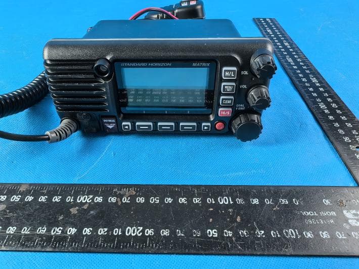
K6630673Y3D
Aug 01, 2024VHF FM Marine Transceiver
Equipment Class
CXX - Communications Rcvr for use w/ licensed Tx and CBs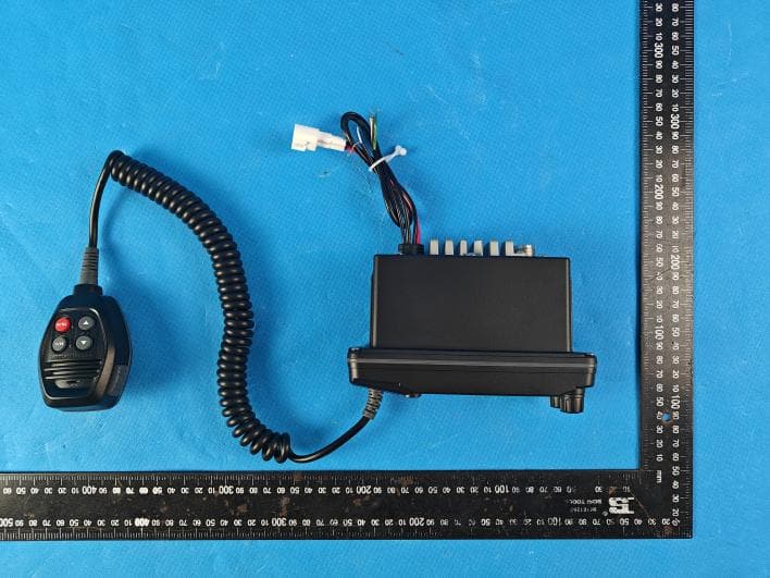
K6630653Y3D
Aug 01, 2024VHF FM Marine Transceiver
Equipment Class
CXX - Communications Rcvr for use w/ licensed Tx and CBs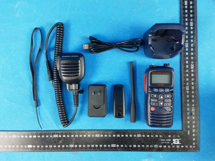
K6630683X30
Jan 10, 2023VHF FM Marine Transceiver
Equipment Class
TNF - Licensed Non-Broadcast Transmitter Held to Face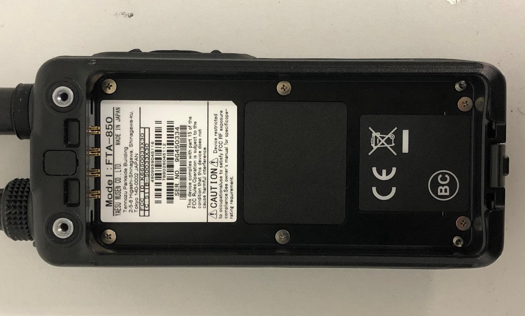
K6650033X30
Nov 18, 2020Airband Radio Transceiver
Equipment Class
TNF - Licensed Non-Broadcast Transmitter Held to Face