K66VXA-700Airband Transceiver
Yaesu Musen Co., Ltd.
Click to zoom
Application Details
- Equipment Class
- TNB - Licensed Non-Broadcast Station Transmitter
- Date of Grant
- Sep 29, 2002
- Application Purpose
- Original Equipment
- Date of Application
- Jul 30, 2002
- Equipment Note
- Airband Transceiver
- Frequency Range
- 118.00000000 - 136.97500000
- Company
- Yaesu Musen Co., Ltd.
- Country
- Japan
Documents & Files
Document Text
Text extracted from the exhibit documents filed with the FCC. Open a document above to read the original.
Users Manual
FCC ID: K66VXA-700 Operating Manual Vertex Standard Co., Ltd. 1 VXA-700 Operating Manual VXA-700 Operating ManualVXA-700 Operating Manual VXA-700 Operating Manual Important Notice! Important Notice!Important Notice! Important Notice! FCC RF Exposure Compliance Requirements for Occupational Use Only: This Radio has been tested and complies with the Federal Communications Commission (FCC) RF exposure limits for Occupational Use/Controlled exposure environment. In addition, it complies with the following Standards and Guidelines: FCC 96-326, Guidelines for Evaluating the Environmental Effects of Radio- Frequency Radiation. FCC OET Bulletin 65 Edition 97-01 (1997) Supplement C, Evaluating Compliance with FCC Guidelines for Human Exposure to Radio Frequency Electromagnetic Fields. ANSI/IEEE C95.1-1992, IEEE Standard for Safety Levels with Respect to Human Exposure to Radio Frequency Electromagnetic Fields, 3 kHz to 300 GHz. ANSI/IEEE C95.3-1992, IEEE Recommended Practice for the Measurement of Potentially Hazardous Electromagnetic Fields - RF and Microwave. This radio is NOT approved for use by the general population in an uncontrolled environment. This radio is restricted to occupational use, work related operations only where the radio operator must have the knowledge to control its RF exposure conditions. When transmitting, hold the radio in a vertical position with its microphone 1 to 2 inches (2.5 to 5 cm) away from your mouth and keep the antenna at least 1 inch (2.5 cm) away from your head and body. The radio must be used with a maximum operating duty cycle not exceeding 50%, in typical Push-to-Talk configurations. DO NOT transmit for more than 50% of total radio use time (50% duty cycle). Transmitting more than 50% of the time can cause FCC RF exposure compliance requirements to be exceeded. The radio is transmitting when the red LED on the top of the radio is illuminated. You can cause the radio to transmit by pressing the P-T-T button. Always use Vertex Standard authorized accessories. NOTICE NOTICENOTICE NOTICE There are no user-serviceable points inside this transceiver. All service jobs must be referred to your Authorized Service Center. FCC ID: K66VXA-700 Operating Manual Vertex Standard Co., Ltd. 2 Introduction IntroductionIntroduction Introduction The Vertex Standard VXA-700 is a compact, stylish, solid hand-held transceiver providing communication (transmit and receive) capability on the International Aircraft Communication Band (“COM” band: 118 ~ 136.975 MHz), and it additionally provides VOR and CDI navigation features on the “NAV” band (108 ~ 117.975 MHz). The VXA-700 includes Temperature display with our exclusive Omni-GlowTM display back-light for minimal degradation of your night vision, NOAA weather band monitoring, 8-character Alpha/Numeric Display, 102 Memory Channels, and 100 “Book Memory” Channels. And the optional Barometric Pressure Unit (SU-1) provides readout of barometric pressure, altitude, and density altitude. We recommend that you read this manual in its entirety, so as to understand the many features of the VXA-700 completely. Keep this manual handy, so you may use it for reference. NOTE NOTENOTE NOTE: The VXA-700’s VOR and CDI Navigation features are supplemental aids to navigation only, and are not intended to be a substitute for accurate (primary) VOR/CDI or landing service equipment. And also, the Barometric/Altitude features of the optional SU-1 are not designed to be a substitute for accurate, calibrated Barometer or Altimeter devices used for navigation critical to personal safety. Congratulations! Congratulations!Congratulations! Congratulations! You now have at your fingertips a valuable communications tool-a Vertex Standard two-way radio! Rugged, reliable and easy to use, your Vertex Standard radio will keep you in constant touch with your colleagues for years to come, with negligible maintenance down-time. Please take a few minutes to read this manual carefully. The information presented here will allow you to derive maximum performance from your radio, in case questions arise later on. We’re glad you joined the Vertex Standard team. Call on us anytime, because communications is our business. Let us help you get your message across. FCC ID: K66VXA-700 Operating Manual Vertex Standard Co., Ltd. 3 Controls & Connectors (Top Panel) Controls & Connectors (Top Panel)Controls & Connectors (Top Panel) Controls & Connectors (Top Panel) 1. Antenna Jack This SMA jack accepts the supplied flexible antenna, or another antenna designed to provide 50 Ohm impedance on the Aircraft Communication Band. 2. MIC/SP Jack You may connect the supplied CT-XX Headset Cable, optional MH-57A4B Speaker/Microphone, or optional CMP460A Waterproof Speaker/Microphone to this jack. Never connect any Speaker/Microphone that is not recommended by the manufacturer. Because these jack connections are unique, using a Speaker/Microphone that is not specified by Vertex Standard may damage the VXA-700. 3. VOLUME Knob This control adjusts the audio volume level. Clockwise rotation increases the volume level. 4. DIAL Selector Knob This 20-position detended rotary switch tunes the operating frequency or selects the memory channels. Controls & Connectors ( Controls & Connectors (Controls & Connectors ( Controls & Connectors (Front FrontFront Front Panel) Panel) Panel) Panel) 1. LCD (Liquid Crystal Display) The display shows the selected operating conditions. 2. PWR Switch Press and hold this switch for 3 seconds to toggle the transceiver’s power on and off. 3. Keypad Several keys have triple functions. The primary functions are labeled on the key top (activated by simply pressing the key momentarily). The secondary functions are labeled in yellow above the top edge of the key (activated by pressing the [F] key first, then the indicated key). FCC ID: K66VXA-700 Operating Manual Vertex Standard Co., Ltd. 4 The third functions are labeled in black above the top edge of the ke…
Text truncated - open the document above for the full version.
External Photos
FCC ID: K66VXA-700 Vertex Standard Co., Ltd. Front view with antenna Rear view with antenna FCC ID: K66VXA-700 Vertex Standard Co., Ltd. Front view without antenna Rear view without antenna FCC ID: K66VXA-700 Vertex Standard Co., Ltd. Left view Right view FCC ID: K66VXA-700 Vertex Standard Co., Ltd. Top view Bottom view FCC ID: K66VXA-700 Vertex Standard Co., Ltd. Labels
ID Label/Location Info
43.543.543.543.5 2 0 . 5 2 0 . 5 2 0 . 5 2 0 . 5 1 6 1 6 1 6 1 6 32323232 3- R1 3- R1 3- R1 3- R1 3 - R 1 .5 3 - R 1 .5 3 - R 1 . 5 3 - R 1 . 5 C 1 .5 C 1 .5 C 1 .5 C 1 .5 C 1 .5 C 1 .5 C 1 .5 C 1 .5 VXA-700VXA-700 LABEL DRAWINGLABEL DRAWING Vertex Standard Co., Ltd.Vertex Standard Co., Ltd. K66VXA-700
Internal Photos
FCC ID: K66VXA-700 Vertex Standard Co., Ltd. Side-A of RF-UNIT Side-B of RF-UNIT with shield case FCC ID: K66VXA-700 Vertex Standard Co., Ltd. Side-B of RF-UNIT without shield case Side-A of AF-UNIT FCC ID: K66VXA-700 Vertex Standard Co., Ltd. Side-B of AF-UNIT Side-A of CNTL-UNIT FCC ID: K66VXA-700 Vertex Standard Co., Ltd. Side-B of CNTL-UNIT Inside chasis
Operational Description
FCC ID: K66VXA-700 Circuit Description Vertex Standard Co., Ltd. 1 VXA-700 Circuit Description Receive Signal Path Narrow FM and AM mode Incoming RF from the antenna jack is passed through a low-pass filter and high-pass filter consisting of coils L1030, L1031, L1035, L1036, L1041 & L1045, capacitors C1142, C1145, C1147, C1153, C1154, C1155, C1159, C1167, C1180, C1182, C1185 & C1186 and antenna switching diodes D1016, D1017 and D1019 (all RLS135 ) to the receiver front end section. Signals within the frequency range of the transceiver is applied to the receiver front end which contains RF amplifier Q1043 ( 2SC5555 ) and varactor-tuned band-pass filter consisting of coils L1022, L1023, L1026, L1027, L1037, L1038, L1043 & L1044, capacitors C1130, C1132, C1134, C1135, C1140, C1143, C1157, C1168, C1175, C1176, C1179 & C1181, and diodes D1014, D1018, D1024 & D1026 (all HVC350 ), then applied to the 1st mixer Q1040 ( 2SC5555 ). Buffered output from the VCO is amplified by Q1017 ( 2SC5555 ) to provide a pure 1st local signal between 143.4 and 199.4 MHz for injection to the 1st mixer. The 35.4 MHz 1st mixer product then passes through monolithic crystal filter XF1001 ( 35M15A1 , 7.5 kHz BW) which strips away all but the desired signal, which is then amplified by mixer postamp Q1033 ( 2SC4215Y ). The amplified 1st IF signal is applied to the AM/FM IF subsystem IC Q2034 ( TK10931V ), which contains the 2nd mixer, 2nd local oscillator, limiter amplifier, noise amplifier and AM/FM detector. A 2nd local signal is generated by PLL reference/2nd local oscillator Q2030 ( 2SC4116GR ) from the 17.475 MHz crystal X2001 The17.475MHz signal is doubled by Q2036 ( 2SC4400 ) to produce the 450 kHz 2nd IF when mixed with the 1st IF signal within Q2034. The 2nd IF then passes through the ceramic filter CF2002 ( ALFYM450) and CF2003 ( CFWM450D ) to strip away unwanted mixer products. In the FM mode, a 2nd IF signal from the ceramic filter CF2002 and CF 2003 applied to the limiter amplifier section of Q2034, which removes amplitude variations in the 450 kHz IF before detection of the speech by the ceramic discriminator CD 2001 ( CDBM450C24 ). Detected audio from Q2034 is passed through the de-emphasis, consisting of the resistors FCC ID: K66VXA-700 Circuit Description Vertex Standard Co., Ltd. 2 R2051, R2053, R2054 & R2101, capacitors C2048, C2049, C2052, C2054 & C2077, and Q2020-2 ( NJM2904V ), then applied to the AF amplifier Q2010 ( TDA7233D ). In the AM mode, detected audio from Q2034 is passed through the audio amplifier Q2020-1 ( NJM2904V ) and ANL circuit, then applied to the AF amplifier Q2020-2 ( NJM2904V ). When impulse noise received, a portion of the AM detector output signal from the AM/FM IF subsystem Q2034, including pulse noise is rectified by D2012 ( BAS316 ). The resulting DC is applied to the ANL MUTE gate Q1019 ( UMG2N ), thus reducing the pulse noises. The processed audio signal from Q2020-2 passes through the audio mute gate Q2014 ( DTC143ZE ) and the volume control to the audio power amplifier Q2010 ( TDA7233D ), providing up to 0.4 Watts to the headphone jack or 8 Ω loudspeaker. A portion of the AF signal from the AM/FM IF subsystem Q2034 converted into DC voltage within the IC, and then passes through the AGC amplifier Q2026 ( UMW1 ) and Q2027 ( 2SA1602A ) to the inversion amplifiers Q1035 and Q1042 (both 2SC5555 ). These amplifier reduce the amplifier gain of the IF amplifier Q1033 and the RF amplifier Q1043 while receiving a strong signal. Wide FM mode Incoming RF from the antenna jack is passed through a low-pass filter and high-pass filter consisting of coils L1030, L1031, L1035, L1036, L1041 & L1045, capacitors C1142, C1145, C1147, C1153, C1154, C1155, C1159, C1167, C1180, C1182, C1185 & C1186 and antenna switching diodes D1016, D1017 and D1019 (all RLS135 ) to the receiver front end section. Signals applied to the wide FM receiver front end which contains RF amplifier Q1041 ( 2SC5555 ) and Q1046 ( 2SC5555 ), varactor-tuned band-pass filter consisting of coils L1017, L1018, L1024, L1025, L1033, L1034, L1039 & L1040, capacitors C1125, C1128, C1129, C1131, C1136, C1148, C1158, C1161, C1162, C1163, & C1169, and diodes D1013, D1015, D1022 & D1025 (all HVC350 ), then applied to the 1st mixer Q1039 ( 2SC5555 ). Buffered output from the VCO is amplified by Q1017 ( 2SC5555 ) to provide a pure 1st local signal between 133.68 and 153.65 MHz for injection to the 1st mixer. The 45.65 MHz FCC ID: K66VXA-700 Circuit Description Vertex Standard Co., Ltd. 3 1st mixer product then passes through band-pass filter consisting of coils L1010 & L1011, capacitors C1075, C1078, C1083, C1087, C1092, & C1093. The 1st IF signal is applied to the wide FM IF subsystem IC Q2023 ( TA7792F ), which contains the 2nd mixer, 2nd local oscillator, limiter amplifier and FM detector. A 2nd local signal is generated by PLL reference/2nd local oscillator Q2030 ( 2SC4116GR ) from the 17.475 MHz crystal X2001. The17.475MHz signal is doubled by Q2036 ( 2SC4400 ) to produce the 10.7 MHz 2nd IF when mixed with the 1st IF signal within Q2023. The 2nd IF then passes through the ceramic filter CF2001 ( SFECV10.7MS2 ) to strip away unwanted mixer products. A flitted 2nd IF signal from the ceramic filter CF2001 applied to the limiter amplifier section of Q2023, which removes amplitude variations in the 10.7MHz IF before detection of the speech by the detect coil L2002, capacitors C2061. Detected audio from Q2023 is passed through the de-emphasis, consisting of the resistors R2051, R2053, R2054 & R2074, capacitors C2048, C2049, C2052, C2054 & C2063, and Q2020-2 ( NJM2904V ), then applied to the AF amplifier Q2010 ( TDA7233D ). Squelch Control When signal is received, appear the DC squelch control voltage at pin 15 of AM/FM IF subsystem Q2034 according to the receiving signal strength. This DC is applied to pin 13 of microprocessor Q3026. The DC squelch control voltage is compared with the SQL threshold level by the microprocessor Q3026…
Text truncated - open the document above for the full version.
Parts List/Tune Up Info
FCC ID: K66VXA-700 Component Applications Location Parts TypeNomenciatureApplication RF-UNIT D 1002DiodeBAS316Ripple Filter D 1003DiodeM1FM3-4063Reverse Voltage Protector D 1004DiodeBAS316Reverse Protector D 1005DiodeHSU277TRFFM Modulater D 1006DiodeBAS316Reverse Rrotector D 1007Varactor DiodeHVC350B-TRFVCO D 1008DiodeHSU277TRFVCO Shift Switch D 1009DiodeRB751S-40TE61DC-DC Converter D 1010DiodeHSU277TRFTX/RX Switch D 1011DiodeMC2848-T11-1TX/RX Switch D 1012DiodeBAS316Reverse Protector D 1013Varactor DiodeHVC350B-TRFBPF Tune D 1014Varactor DiodeHVC350B-TRFBPF Tune D 1015Varactor DiodeHVC350B-TRFBPF Tune D 1016DiodeRLS135 TE-11Antenna Switch D 1017DiodeRLS135 TE-11Antenna Switch D 1018Varactor DiodeHVC350B-TRFBPF Tune D 1019DiodeRLS135 TE-11Antenna Switch D 1020DiodeRN739F T106RF Level Limitter D 1021DiodeHSM88WA TRPower Detect D 1022Varactor DiodeHVC350B-TRFBPF Tune D 1023DiodeDAN235U TLBand Switch D 1024Varactor DiodeHVC350B-TRFBPF Tune D 1025Varactor DiodeHVC350B-TRFBPF Tune D 1026Varactor DiodeHVC350B-TRFBPF Tune D 1027DiodeBAS316Reverse Protector D 1028DiodeBAS316Power Detect Q 1001Transistor2SC4116GR TE85RRipple Filter Q 1002TransistorRT1N241M-T11-1FM Mod. Mute Switch Q 1004TransistorDTA143EE TLVCO Save Switch Q 1006TransistorDTA143EE TLRX Save Switch Q 1007TransistorDTA143EE TLRX Switch Q 1009TransistorRT1P441U-T11-1PLL Save Switch Q 1010TransistorRT1N241M-T11-1VCO Shift Switch Q 1011Transistor2SB1132 T100 Q3.5V Regulator Q 1012TransistorUMW1N TR3.5V Regulator Q 1013ICMB15A01PFV1-G-BND-EFPLL Sbsystem Q 1014Transistor2SC5555ZD-TRVCO Q 1015ICRH5RH651A-T1DC-DC Converter Q 1016Transistor2SA1602A-T11-1FTX Unlock Switch Q 1017Transistor2SC5555ZD-TRBuffer Amplifier Q 1018TransistorUMW1N TRTX Unlock Switch Q 1019Transistor2SK880GR TE85VCV Buffer Q 1020TransistorDTA143EE TLTX Unlock Switch Q 1021Transistor2SC5555ZD-TRBuffer Amplifier Q 1022TransistorUMW1N TRTX Regulator Q 1023TransistorDTA143EE TLTX AM/FM Switch Q 1024Transistor2SB1132 T100 QTX Regulator Q 1025TransistorUMD2N TRTX Amp. Gain Control Switch Q 1026TransistorUMD2N TRTX AM/FM Switch Q 1029Transistor2SC3356-T2B R25Driver Amplifier Q 1030TransistorRT1N241M-T11-1TX Amp. Gain Control Switch Q 1031FET2SK2973-T13Exciter Amplifier Q 1032Transistor2SA1602A-T11-1FAGC Amplifier Q 1033Transistor2SC4215Y TE85RIF Amplifier Q 1034TransistorUMW1N TRAGC Amplifier Q 1035Transistor2SC5555ZD-TRAGC Q 1037FET2SK2974-T11Power Amplifier Q 1038Transistor2SC5555ZD-TRAGC Q 1039Transistor2SC5555ZD-TR1st Mixer Vertex Standard Co., Ltd. FCC ID: K66VXA-700 Component Applications Location Parts TypeNomenciatureApplication Q 1040Transistor2SC5555ZD-TR1st Mixer Q 1041Transistor2SC5555ZD-TRRF Amplifier Q 1042Transistor2SC5555ZD-TRAGC Q 1043Transistor2SC5555ZD-TRRF Amplifier Q 1044TransistorRT1N241M-T11-1WFM VCV Switch Q 1045TransistorRT1N241M-T11-1AM Mod. Mute Switch Q 1046Transistor2SC5555ZD-TRRF Amplifier Q 1047TransistorRT1N241M-T11-1VCO Shift Switch AF-UNIT D 2001DiodeBAS316Reverse Protector D 2002DiodeBAS316Reverse Protector D 2004DiodeMC2850-T11-1Voltage Control D 2005DiodeMC2850-T11-1Reverse Protector D 2009Zener DiodeRD6.8UMB2-T1BVoltage Control D 2012DiodeBAS316ANL D 2013DiodeBAS316REF Frequency Compensation D 2014Varactor DiodeHVU202A-TRDCS Modulater D 2015Varactor DiodeMA376-(TX)REF Frequency Compensation D 2016Varactor DiodeHVC350B-TRFReference Oscillator D 2017DiodeBAS316AGC D 2018DiodeMC2848-T11-1CF Switch D 2019DiodeMC2848-T11-1CF Switch D 2020DiodeDAN235U TL2nd Local Switch D 2021Diode1SS302 TE85RSQS Detector D 2022DiodeMC2850-T11-1Fast Switch D 2023DiodeMC2850-T11-1Fast Switch D 2024DiodeBAS316Detector D 2025DiodeBAS316VOR Switch D 2026DiodeBAS316Reverse Protector Q 2001TransistorUMZ2N TRPTT Switch Q 2002FET2SJ364-R(TX)WX Arert Switch Q 2005Transistor2SB1132 T100 QMic Amp. Regulator Q 2006TransistorRT1N241M-T11-1Mic Amp. REG Switch Q 2008TransistorRT1N241M-T11-1AF Mute Switch Q 2009TransistorRT1N241M-T11-1AF Mute Switch Q 2010IC TDA7233D-TRAF Power Amplifier Q 2012Transistor2SB1132 T100 QAF Amp. Control Switch Q 2013Transistor2SC4116GR TE85RAF Amp. Control Switch Q 2014TransistorDTC143ZE TLAF Mute Switch Q 2015TransistorDTA143EE TLRX Wide/Narrow Switch Q 2016TransistorRT1N241M-T11-1RX AM/FM Switch Q 2017TransistorRT1N241M-T11-1RX Wide/Narrow Switch Q 2018TransistorDTA143EE TLRX Wide/Narrow Switch Q 2019TransistorUMG2N TRANL Switch Q 2020IC NJM2904V-TE1AF Amplifier Q 2021TransistorRT1N241M-T11-1SQS Switch Q 2022FETHN1J02FU(TE85L)AF Wide/Narrow Switch Q 2023IC TA7792F(TP1)IF Subsystem (Wide) Q 2024Transistor2SA1602A-T11-1FAGC Switch Q 2025Transistor2SC4116GR TE85RSQS Amplifier Q 2026TransistorUMW1N TRAGC Amplifier Q 2027Transistor2SA1602A-T11-1FAGC Amplifier Q 2028TransistorRT1N241M-T11-1CF Switch Q 2029Transistor2SC4116GR TE85RAGC Switch Q 2030Transistor2SC4116GR TE85RReference Oscillator Q 2031Transistor2SC4116GR TE85RSQS Amplifier Q 2032TransistorDTC143ZE TLAGC Switch Q 2033Transistor2SC4116GR TE85RSQS Amplifier Q 2034IC TK10931VT1IF Subsystem (Narrow) Q 2035TransistorRT1N241M-T11-1AGC Switch Q 2036Transistor2SC4400-4-TLDoubler Vertex Standard Co., Ltd. FCC ID: K66VXA-700 Component Applications Location Parts TypeNomenciatureApplication Q 2037IC NJM2902V-TE1VOR Q 2038IC NJM2901V-TE1VOR CNTL-UNIT D 3002DiodeBAS316Reverse Protector D 3003LEDFRGB1312CE-10-TFTX/BUSY Lamp D 3005DiodeBAS316Reverse Protector D 3006DiodeBAS316AM Mod. Mute Switch D 3007DiodeRN739F T106Modulation Atteneter D 3009DiodeBAS316FM Mod. Mute Switch D 3010DiodeBAS316Modulation Atteneter Switch D 3012LEDSPMA10-1104Q7NCIllumination D 3013LED19-215UYOC/S530A2/TR8Illumination D 3014LED19-215UYOC/S530A2/TR8Illumination D 3015LED19-215UYOC/S530A2/TR8Illumination D 3017LED19-215UYOC/S530A2/TR8Illumination D 3018LEDSPMA10-1104Q7NCIllumination D 3019LED19-215UYOC/S530A2/TR8Illumination D 3020LED19-215UYOC/S530A2/TR8Illumination D 3021LED19-215UYOC/S530A2/TR8Illumination D 3023DiodeMC2850-T11-1Reset Control D 3024Zener DiodeHZU4ALL-TRVoltage Protector D 3025DiodeBAS316Voltage Protector D …
Text truncated - open the document above for the full version.
Parts List/Tune Up Info
FCC ID: K66VXA-700 Alignment Vertex Standard Co., Ltd. 1 VXA-700 Alignment VXA-700 AlignmentVXA-700 Alignment VXA-700 Alignment Introduction IntroductionIntroduction Introduction The VXA-700 is carefully aligned at the factory for the specified performance across the Aircraft and Weather bands. Realignment should therefore not be necessary except in the event of a component failure. The following procedures cover the adjustments that are not normally required once the transceiver has left the factory. However, if damage occurs and some parts subsequently are replaced, realignment may be required. If a sudden problem occurs during normal operation, it is likely due to component failure; realignment should not be done until after the faulty component has been replaced. We recommend that servicing be performed only by authorized Vertex Standard service technicians who are experienced with the circuitry and fully equipped for repair and alignment. If a fault is suspected, contact the dealer from whom the transceiver was purchased for instructions regarding repair. Under no circumstances should any alignment be attempted unless the normal function and operation of the transceiver are clearly understood, the cause of the malfunction has been clearly pinpointed and any faulty components replaced, and realignment determined to be absolutely necessary. Problems caused by unauthorized attempts at realignment are not covered by the warranty policy Vertex Standard reserves the right to change circuits and alignment procedures, in the interest of improved performance, without notifying owners. The following test equipment (and familiarity with its use) is necessary for complete realignment. While most steps do not require all of the equipment listed, the interactions of some adjustments may require that more complex adjustments be performed afterwards. Do not attempt to perform only a signal step unless it is clearly isolated electrically from all other steps. Have all test equipment ready before beginning, and follow all of the steps in a section in the order presented. Correction of problems caused by misalignment resulting from use of improper test equipment is not covered under the warranty policy. FCC ID: K66VXA-700 Alignment Vertex Standard Co., Ltd. 2 Required Test Equipment Required Test EquipmentRequired Test Equipment Required Test Equipment ο Radio Tester with calibrated output level at 200 MHz ο In-line Wattmeter with 5% accuracy at 200 MHz ο 50- Ω , 10-W RF Dummy Load ο Regulated DC Power Supply adjustable from 3 to 15 VDC, 2A ο Frequency Counter: ±0.2 ppm accuracy at 200 MHz ο AF Signal Generator ο AC Voltmeter ο DC Voltmeter: high impedance ο VHF Sampling Coupler Alignment Preparation & Precautions Alignment Preparation & PrecautionsAlignment Preparation & Precautions Alignment Preparation & Precautions A 50- Ω RF load and in-line wattmeter must be connected to the main antenna jack in all procedures that call for transmission, except where specified otherwise. Correct alignment is not possible with an antenna. After completing one step, read the next step to see if the same test equipment is required. If not, remove the test equipment (except dummy load and wattmeter, if connected) before proceeding. Correct alignment requires that the ambient temperature be the same as that of the transceiver and test equipment, and that this temperature be held constant between 20 ~ 30 °C (68 ~ 86 °F). When the transceiver is brought into the shop from hot or cold air, it should be allowed some time to come to room temperature before alignment. Whenever possible, alignments should be made with oscillator shields and circuit boards firmly affixed in place. Also, the test equipment must be thoroughly warmed up before beginning. Set up the test equipment as shown below for transceiver alignment, apply 7.2 VDC power to the transceiver. Notes: signal levels in dB Notes: signal levels in dB Notes: signal levels in dB Notes: signal levels in dB referred referredreferred referred to in alignment are based on 0 dB to in alignment are based on 0 dB to in alignment are based on 0 dB to in alignment are based on 0 dBμ = μ = μ = μ = 0.5 0.5 0.5 0.5 μV (closed μV (closedμV (closed μV (closed circuit). circuit).circuit). circuit). PLL Section PLL SectionPLL Section PLL Section PLL Reference Frequency ! Connect the wattmeter, dummy load and frequency counter connected to the FCC ID: K66VXA-700 Alignment Vertex Standard Co., Ltd. 3 antenna jack, then set the transceiver to 128.000 MHz and turn the transceiver off. ! Press and hold in the PTT switch, Monitor switch, and [MW(SPL.W)] key while turn the transceiver on to enter the alignment mode. ! Rotate the DIAL selector knob to select the “RX TUNE xxx.” ! Press the PTT switch, confirm the counter reading is 128.000 MHz. ! If not, 1. press the [SEL(SET)] key momentarily, 2. rotate the DIAL selector knob clockwise (frequency up) or counter-clockwise (frequency down), 3. press the [SEL(SET)] key again, 4. confirm the counter reading. ! Repeat above steps 1 - 4, so that the counter reading is 128.000 MHz (±100 Hz). ! Turn the transceiver off. Transmitter Section Transmitter SectionTransmitter Section Transmitter Section AM TX HI Power Adjustment ! Connect the wattmeter and dummy load to the antenna jack, then set the transceiver to 128.000 MHz and turn the transceiver off. ! Press and hold in the PTT switch, Monitor switch, and [MW(SPL.W)] key while turn the transceiver on to enter the alignment mode. ! Rotate the DIAL selector knob to select the “AM TX Hi xxx.” ! Press the PTT switch with no microphone input, confirm the RF output power is 1.5 Watts. ! If not, 1. press the [SEL(SET)] key momentarily, 2. rotate the DIAL selector knob clockwise (increase the power) or counter- clockwise (decrease the power), 3. press the [SEL(SET)] key again, 4. confirm the RF output power. ! Repeat above steps 1 - 4, so that the RF output power is 1.5 Watts. ! Turn the transceiver off. A…
Text truncated - open the document above for the full version.
RF Exposure Info
CELLTECH RESEARCH INC.Test Report S/N: 072202-264K66 1955 Moss Court, KelownaTest Date(s): July 22, 2002 B.C. Canada V1Y 9L3 FCC/IC SAR Evaluation © 2002 Celltech Research Inc.1 of 20 DECLARATION OF COMPLIANCE SAR EVALUATION Celltech Research Inc. declares under its sole responsibility that this device was found to be in compliance with the Specific Absorption Rate (SAR) RF exposure requirements specified in FCC §2.1093 and Health Canada’s Safety Code 6. The device was tested in accordance with the measurement standards and procedures specified in FCC OET Bulletin 65, Supplement C, Edition 01-01 and Industry Canada RSS-102 Issue 1 (General Population/Uncontrolled Exposure). I attest to the accuracy of data. All measurements were performed by me or were made under my supervision and are correct to the best of my knowledge and belief. I assume full responsibility for the completeness of these measurements and vouch for the qualifications of all persons taking them. This test report shall not be reproduced partially, or in full, without the prior written approval of Celltech Research Inc. The results and statements contained in this report pertain only to the device(s) evaluated. Russell W. Pipe Senior Compliance Technologist Celltech Research Inc. Test Lab CELLTECH RESEARCH INC. Testing and Engineering Lab 1955 Moss Court Kelowna, B.C. Canada V1Y 9L3 Phone: 250 - 860-3130 Fax: 250 - 860-3110 e-mail: [email protected] web site: www.celltechlabs.com Applicant Information VERTEX STANDARD CO., LTD. 4-8-8, Nakameguro, Meguro-Ku Tokyo 153-8644, Japan Rule Part(s):FCC §2.1093; IC RSS-102 Issue 1 (Provisional) Test Procedure(s):FCC OET Bulletin 65 Supplement C (01-01) FCC ID:K66VXA-700 Model:VXA-700 EUT Type:Portable AirBand PTT Radio Transceiver Modulation:AM Tx Frequency Range:118 - 136.975 MHz RF Conducted Power Tested:31.73 dBm (118.000 MHz) 31.76 dBm (128.000 MHz) 31.78 dBm (136.975 MHz) Antenna Type(s):Whip Battery Type(s):7.4V Lithium-ion (1300mAh) Body-Worn Accessories:Belt-Clip, Speaker-Microphone CELLTECH RESEARCH INC.Test Report S/N: 072202-264K66 1955 Moss Court, KelownaTest Date(s): July 22, 2002 B.C. Canada V1Y 9L3 FCC/IC SAR Evaluation © 2002 Celltech Research Inc.2 of 20 TABLE OF CONTENTS 1.0INTRODUCTION.................................................................. 3 2.0DESCRIPTION OF EUT......................................................... 3 3.0SAR MEASUREMENT SYSTEM ............................................. 4 4.0MEASUREMENT SUMMARY..................................................5-6 5.0DETAILS OF SAR EVALUATION............................................ 7 6.0EVALUATION PROCEDURES................................................. 7 7.0SYSTEM VALIDATION.......................................................... 8 8.0TISSUE PARAMETERS......................................................... 8 9.0SIMULATED EQUIVALENT TISSUES...................................... 9 10.0SAR LIMITS........................................................................ 9 11.0SYSTEM SPECIFICATIONS.................................................... 10 12.0PROBE SPECIFICATION....................................................... 11 13.0SMALL PLANAR PHANTOM................................................... 11 14.0LARGE PLANAR PHANTOM.................................................... 11 15.0DEVICE HOLDER................................................................. 11 16.0TEST EQUIPMENT LIST........................................................ 12 17.0MEASUREMENT UNCERTAINTIES........................................ 13 18.0REFERENCES...................................................................... 14 APPENDIX A - SAR MEASUREMENT DATA......................................... 15 APPENDIX B - SYSTEM VALIDATION................................................ 16 APPENDIX C - DIPOLE CALIBRATION................................................ 17 APPENDIX D - PROBE CALIBRATION................................................ 18 APPENDIX E - MEASURED FLUID DIELECTRIC PARAMETERS............. 19 APPENDIX F - SAR TEST SETUP & EUT PHOTOGRAPHS...................... 20 CELLTECH RESEARCH INC.Test Report S/N: 072202-264K66 1955 Moss Court, KelownaTest Date(s): July 22, 2002 B.C. Canada V1Y 9L3 FCC/IC SAR Evaluation © 2002 Celltech Research Inc.VERTEX STANDARD CO., LTD. FCC ID: K66VXA-7003 of 20 Portable AM AirBand PTT Radio Transceiver (118-136.975MHz) 1.0 INTRODUCTION This measurement report demonstrates that the VERTEX STANDARD CO., LTD. Model: VXA-700 Portable AM AirBand PTT Radio Transceiver FCC ID: K66VXA-700 complies with FCC 47 CFR §2.1093 (see reference [1]) and Health Canada Safety Code 6 (see reference [2]). The test procedures described in FCC OET Bulletin 65, Supplement C, Edition 01-01 (see reference [3]) and IC RSS-102 Issue 1 (Provisional) (see reference [4]), were employed. A description of the product and operating configuration, detailed summary of the test resu…
Text truncated - open the document above for the full version.
Contact Information
Applicant
Masatoshi Muraishi(Engineering Division)
Technical Contact
M. Flom Associates, IncMorton Flom
[email protected]480 926 3100
3356 N. San Marcos Pl., Suite 107 · Chandler, Arizona · United States
Non-Technical Contact
M. Flom Associates, Inc.Morton Flom
[email protected]480 926 3100
Test Firm
M. Flom Associates, Inc.Morton Flom
Technical Specifications
| # | Rule Parts | Frequency Range | Power Output | Emission | Tolerance |
|---|---|---|---|---|---|
| 1 | 87 | 118 MHz - 136.975 MHz | 1.5 W | 8K00A3E | 10.0000000000 ppm |
Other Applications from Yaesu Musen Co., Ltd.
K660E180X10
Dec 01, 2025BLUETOOTH MICROPHONE
Equipment Class
DTS - Digital Transmission System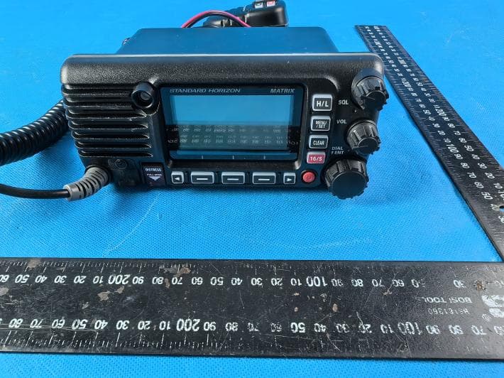
K6630673Y3D
Aug 01, 2024VHF FM Marine Transceiver
Equipment Class
CXX - Communications Rcvr for use w/ licensed Tx and CBs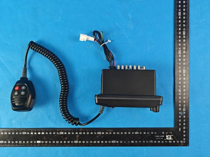
K6630653Y3D
Aug 01, 2024VHF FM Marine Transceiver
Equipment Class
CXX - Communications Rcvr for use w/ licensed Tx and CBs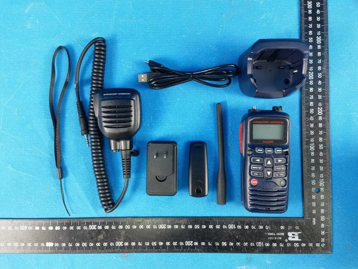
K6630683X30
Jan 10, 2023VHF FM Marine Transceiver
Equipment Class
TNF - Licensed Non-Broadcast Transmitter Held to Face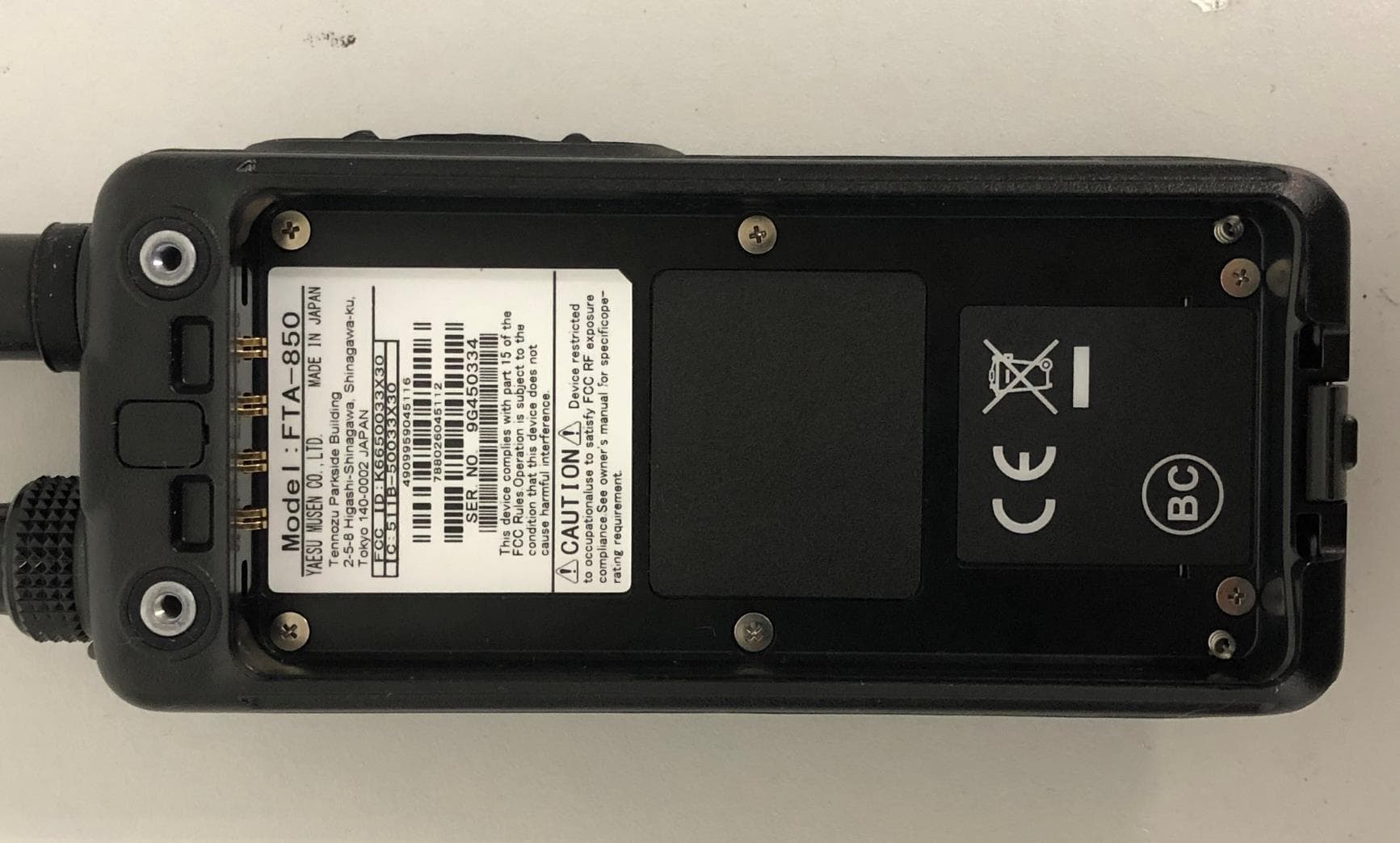
K6650033X30
Nov 18, 2020Airband Radio Transceiver
Equipment Class
TNF - Licensed Non-Broadcast Transmitter Held to Face