L5ACMDM4DUAL MODE CELLULAR PHONE (AMPS/CDMA)
Sony Electronics Inc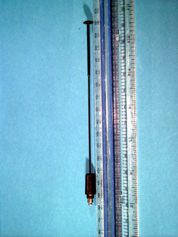
Click to zoom
Application Details
- Equipment Class
- TNE - Licensed Non-Broadcast Transmitter Held to Ear
- Date of Grant
- Dec 10, 1998
- Application Purpose
- Original Equipment
- Date of Application
- Oct 08, 1998
- Equipment Note
- DUAL MODE CELLULAR PHONE (AMPS/CDMA)
- Frequency Range
- 824.02000000 - 848.98000000
- Company
- Sony Electronics Inc
- Country
- United States
Documents & Files
Document Text
Text extracted from the exhibit documents filed with the FCC. Open a document above to read the original.
Users Manual
Operating Instructions CM-M1300 CM-M2300 CM-M3300 Digital Portable Cellular Telephone 3-861-740-11 (2) 80-68301-1 Rev A CM-M1300_01_07final3/2/98, 11:40 AM1 2 Before operating the your portable telephone, please read this manual thoroughly and retain it for future reference. If your usage includes in-vehicle operation, it is recommended that you refer to the Installation/Connections/Operation manual for the optional accessory kits. WARNING To prevent fire or shock hazard, do not expose the unit to rain or moisture. FCC CAUTION STATEMENT You are cautioned that any changes or modifications not expressly approved in this manual could void your authority to operate this equipment. Owner’s record The model number, regulatory number, and serial number are located on a nameplate inside the battery compartment. Record the serial number in the space provided below. Refer to these numbers whenever you call your dealer regarding this product. Model No.: ___________________Serial No.: _________________ DISPOSAL OF LITHIUM ION BATTERY LITHIUM ION BATTERY. DISPOSE OF PROPERLY. You can return your unwanted lithium ion batteries to your nearest Sony Service Center or Factory Service Center. Note:In some areas the disposal of lithium ion batteries in household or business trash may be prohibited. For the Sony Service Center nearest you call 1-800-222-SONY (United States only). For the Sony Factory Service Center nearest you call 416-499-SONY (Canada only). ® ©1997 Sony Electronics Inc. All rights reserved. Reproduction without written consent expressly prohibited. Sony and Jog Dial are trademarks of Sony. All other trademarks are the property of their respective owners. Design and specifications are subject to change without notice. Talk and standby times are subject to change. CM-M1300_01_07final3/2/98, 11:40 AM2 3 Rules and regulations The U.S. Federal Communications Commission and the Industry Canada regulate cellular telephone service in their respective countries. It is important for you, the cellular telephone user, to observe the applicable regulations when operating your cellular telephone in either country. In addition to these U.S. and Canadian federal regulations, you may be bound also by certain state, provincial, territorial, and local rules and regulations, as well as by your cellular carrier’s tariff (the rates, terms, and conditions of its service). If you wish to use your cellular telephone in both the U.S. and Canada, please consult with your System Operator. Furthermore, you should remember that your cellular telephone is a radiotelephone, — i.e., it combines both wireline technology, as used in your home or office telephone system, and radio technology — and that the scope of regulations and precautions is therefore broader than the scope of regulations and precautions relating to wireline-only telephone usage. Some of the major points of consideration are set out below. Please note, however, that these “Rules and Regulations" and "Safety Precautions” sections do not constitute legal advice, and are intended merely for general information purposes. If you have specific questions, please contact your cellular carrier (System Operator). License — If your home system is in the U.S., you do not require a separate license to operate your cellular telephone; obtaining a cellular telephone access number is sufficient to register you as a user. If your home system is in Canada, a separate license is required; your carrier will assist you in the licensing process. If you wish to use your cellular phone on both sides of the border, please contact your cellular carrier (System Operator). Equipment modifications — The U.S. Federal Communications Commission has type-approved the model of cellular telephone which you have purchased, and has allocated a specific frequency range for cellular service. No changes or adjustments are to be made to your cellular telephone. The radio equipment shall be made available for inspection upon request by representatives of the FCC or licensees. Denial of service — A cellular carrier may deny service temporarily or terminate service for violation of any government regulations or violation of its tariff. Privacy — As a telephone user, you have come to assume a certain standard of privacy when you place or receive a telephone call via the traditional wireline systems. However, because cellular telephones utilize radio transmissions to effect calls, the same standard cannot always be assured. While it is unlawful for any unauthorized person to divulge or use any information obtained from intercepting or “listening in on” conversations intended for others, you should not assume that your conversation is completely secure. Commercially available scanning equipment can permit a third party to monitor the radio channels used for cellular telephone calls. Interference — No person shall interfere with, or cause interference to, any radio communication or signal. CM-M1300_01_07final3/2/98, 11:40 AM3 4 The Institute of Electrical and Electronics Engineers (IEEE) in 1991, and The American National Standards Institute (ANSI) in 1992, updated the 1982 ANSI Standard for safety levels with respect to human exposure to RF energy. Over 120 scientists, engineers, and physicians from universities, government health agencies, and industry, reviewed the available research and developed this updated Standard. In March 1993, the U.S. Federal Communications Commission (FCC) proposed the adoption of this updated Standard. The design of your phone complies with this updated Standard. Of course, if you want to limit RF exposure even further than the updated ANSI Standard, you may choose to control the duration of your calls and operate your phone in the most power efficient manner. Efficient phone operation For your phone to operate at the lowest power level consistent with satisfactory call quality, please observe the following guidelines: Your phone has an extendable antenna; extend it ful…
Text truncated - open the document above for the full version.
Users Manual
4 The Institute of Electrical and Electronics Engineers (IEEE) in 1991, and The American National Standards Institute (ANSI) in 1992, updated the 1982 ANSI Standard for safety levels with respect to human exposure to RF energy. Over 120 scientists, engineers, and physicians from universities, government health agencies, and industry, reviewed the available research and developed this updated Standard. In March 1993, the U.S. Federal Communications Commission (FCC) proposed the adoption of this updated Standard. The design of your phone complies with this updated Standard. Of course, if you want to limit RF exposure even further than the updated ANSI Standard, you may choose to control the duration of your calls and operate your phone in the most power efficient manner. Efficient phone operation For your phone to operate at the lowest power level consistent with satisfactory call quality, please observe the following guidelines: Your phone has an extendable antenna; extend it fully whenever possible for maximum efficiency. Hold the phone as you would any other telephone. While speaking directly into the mouthpiece, position the antenna up and over your shoulder. Do not hold the antenna when the phone is in use. Holding the antenna affects call quality and may cause the phone to operate at a higher power level than needed. Safety precautions IMPORTANT For safe and efficient operation of your phone, observe these guidelines. Your dual mode (analog/digital CDMA) hand-held portable cellular telephone uses both analog frequency modulation (FM) technology and digital Code Division Multiple Access (CDMA) technology. CDMA is a newer radio frequency (RF) technology than the FM technology that has been used for radio communications for decades. Your dual mode portable cellular telephone is a radio transmitter and receiver. When the phone is ON, it receives and sends out radio frequency (RF) energy. The phone operates in the frequency range of 824 MHz to 894 MHz. When you use your phone, the cellular system handling your call controls the mode of operation (analog or digital CDMA) and the power level at which your phone transmits. In the analog mode, the power is continuously transmitted at a level that can range from 6 mW to 600 mW. In the digital CDMA mode, the power is transmitted as a digitally coded waveform at a rate varying from 100 Hz to 800 Hz. The average power can range from 0.01 μW to 420 mW. Exposure to radio frequency energy Research on health effects from RF energy has focused for many years on FM radio technology. That research and studies regarding newer radio technologies, such as CDMA, have found no credible scientific evidence that adverse health effects result from the use of cellular telephones. CM-M1300_01_07final 3/2/98, 11:40 AM4 77 Additional Information Specifications Frequency range Transmit: 824.04 to 848.97 MHz Receive: 869.04 to 893.97 MHz Dimensions 5.7 × 2.0 × 1.5 inches (h/w/d) (not including antenna) (146 × 50 × 37 mm) Mass (weight) Approx. 7.2 oz (203 g) (including battery) RF power output CDMA: 0.01 μW to 420 mW FM: 6 mW to 600 mW Operational temperature–22°F to +140°F (–30°C to +60°C) (excluding battery pack) Supplied accessories QN-003BPLH Hi-Cap Li-Ion Battery Pack (1) QN-001AC AC Adapter (1) Hand strap (1) Optional accessories QN-002BCD Dual Slot Battery Charger QN-003BPLH Hi-Cap Li-Ion Battery Pack QN-004BPLS Slim Li-Ion Battery Pack QN-005BPNM Ni-MH Battery Pack QN-006BPNC Ni-Cd Battery Pack QN-007HFK Hands-Free Car Kit QN-008CLA Rapid Charging Cigarette Lighter Adapter QN-009TA Travel Adapter QN-010LC Carrying Case (for CM-M1300, B1200, S1100 series telephones) QN-011PH Hands-Free Privacy Handset QN-012DA Data Cable QN-013HC Auto Travel Holder QN-016SKT Starter Kit (QN-010LC Carrying Case, Single Slot Charging Stand, Rapid Charging Cigarette Lighter Adapter) QN-017SKT Starter Kit (QN-019LC Carrying Case, Single Slot Charging Stand, Rapid Charging Cigarette Lighter Adapter) QN-018SKT Starter Kit (QN-018LC Carrying Case, Single Slot Charging Stand, Rapid Charging Cigarette Lighter Adapter) QN-018LC Carrying Case (for CM-M2300, B2200, S2100 series telephones) QN-019LC Carrying Case (for CM-M3300, B3200, S3100 series telephones) QN-020TCL Combination Travel Adapter/Cigarette Lighter Adapter QN-025PHK Portable Hands-Free Car Kit Call 1-800-488-SONY (7669) to order additional accessories (USA only). Design and specifications are subject to change without notice. CM-M1300_74_84final 3/2/98, 12:00 PM77
Attestation Statements
Sony Electronics Inc., Personal & Mobile Communications of America 16450 West Bernardo Drive, San Diego, California 92127-1804 Telephone (619) 487-8500 Federal Communications Commission October 9, 1998 Authorization and Evaluation Division Equipment Authorization Branch 7435 Oakland Mills Road Columbia, MD 21046 In Re: Sony Electronics, Inc. FCC ID: L5ACMDM4 Dual Mode Portable Cellular Phone (AMPS/CDMA) Request for Confidentiality Gentlemen: In accordance with 0.459 of CFR 47, SONY ELECTRONICS, Inc. requests confidentiality of the Block Diagram & Schematics for the attached test report. These documents contain detailed system and equipment description and related information about the product which SONY ELECTRONICS, Inc. considers to be proprietary, confidential, and a custom design and, otherwise, would not release to the general public. Since this design is a basis from which future technological products will evolve, SONY ELECTRONICS, Inc. feels that this information would be of benefit to its competitors, and that the disclosure of the information in these documents would give our competitors an unfair advantage in the market. Sincerely, Glen A. Seebruch Regulatory Engineer Sony PMC America
Attestation Statements
Sony Electronics Inc., Personal & Mobile Communications of America 16450 West Bernardo Drive, San Diego, California 92127-1804 Telephone (619) 487-8500 October 9, 1998 AFFIDAVIT FOR ESN PROTECTION OF CELLULAR MOBILE TELEPHONES We hereby certify that the Handheld Portable Cellular Telephone, FCC ID: _ L5ACMDM4__ is so designed that it complies with all the requirements for ESN protection specified in Section 22.919 CFR 47. Sec. 22.919 Electronic serial numbers. The Electronic Serial Number (ESN) is a 32 bit binary number that uniquely identifies a cellular mobile transmitter to any cellular system. (a) Each mobile transmitter in service must have a unique ESN. (b) The ESN host component must be permanently attached to a main circuit board of the mobile transmitter and the integrity of the unit's operating software must not be alterable. The ESN must be isolated from fraudulent contact and tampering. If the ESN host component does not contain other information, that component must not be removable, and its electrical connections must not be accessible. If the ESN host component contains other information, the ESN must be encoded using one or more of the following techniques: (1) Multiplication or division by a polynomial; (2) Cyclic coding; (3) The spreading of ESN bits over various non-sequential memory locations. (c) The ESN must be factory set and must not be alterable, transferable, removable or otherwise able to be manipulated. Cellular mobile equipment must be designed such that any attempt to remove, tamper with, or change the ESN chip, its logic system, or firmware originally programmed by the manufacturer will render the mobile transmitter inoperative. Sincerely, Glen A. Seebruch Regulatory Engineer Sony PMC America
External Photos
Test Report S/N: SAR.980914637.L5ASAR Measurement Report Test Date(s): October 19-23, 1998FCC Part 22 Certification © 1998 PCTEST LabFCC ID: L5ACMDM4 NVLAP Lab Code: 100431-0 SONY Electronics, Inc. 1 1 Peak SAR Value at the surface of the phantom @ Z=0 (not averaged over 1-gram of tissue). This is a computer simulation of the hot spot(s) of the phone. Test Report S/N: 22.980914636.L5AFCC Part 22 Test Date(s): October 19-23, 1998Certification © 1998 PCTEST LabFCC ID: L5ACMDM4 NVLAP Lab Code: 100431-0 SONY Electronics, Inc. Test Report S/N: 22.980914636.L5AFCC Part 22 Test Date(s): October 19-23, 1998Certification © 1998 PCTEST LabFCC ID: L5ACMDM4 NVLAP Lab Code: 100431-0 SONY Electronics, Inc. Test Report S/N: 22.980914636.L5AFCC Part 22 Test Date(s): October 19-23, 1998Certification © 1998 PCTEST LabFCC ID: L5ACMDM4 NVLAP Lab Code: 100431-0 SONY Electronics, Inc. Test Report S/N: 22.980914636.L5AFCC Part 22 Test Date(s): October 19-23, 1998Certification © 1998 PCTEST LabFCC ID: L5ACMDM4 NVLAP Lab Code: 100431-0 SONY Electronics, Inc. Test Report S/N: 22.980914636.L5AFCC Part 22 Test Date(s): October 19-23, 1998Certification © 1998 PCTEST LabFCC ID: L5ACMDM4 NVLAP Lab Code: 100431-0 SONY Electronics, Inc. Test Report S/N: 22.980914636.L5AFCC Part 22 Test Date(s): October 19-23, 1998Certification © 1998 PCTEST LabFCC ID: L5ACMDM4 NVLAP Lab Code: 100431-0 SONY Electronics, Inc.
ID Label/Location Info
© 1998 PCTEST Lab FCC ID SAMPLE LABEL LOCATION LABELLING REQUIREMENTS PER §§ 2.925 The Label shown shall be permanently affixed at a conspicuous location on the device and be readily visible to the user at the time of purchase. Fig 12. Sample label FCC ID: L5ACMDM4
Internal Photos
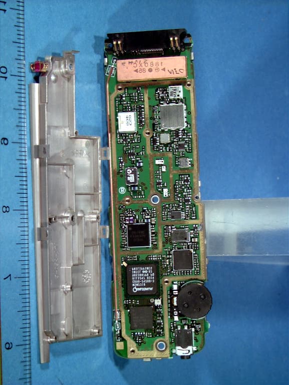
Test Report S/N: 22.980914636.L5AFCC Part 22 Test Date(s): October 19-23, 1998Certification © 1998 PCTEST LabFCC ID: L5ACMDM4 NVLAP Lab Code: 100431-0 SONY Electronics, Inc. Test Report S/N: 22.980914636.L5AFCC Part 22 Test Date(s): October 19-23, 1998Certification © 1998 PCTEST LabFCC ID: L5ACMDM4 NVLAP Lab Code: 100431-0 SONY Electronics, Inc. Test Report S/N: 22.980914636.L5AFCC Part 22 Test Date(s): October 19-23, 1998Certification © 1998 PCTEST LabFCC ID: L5ACMDM4 NVLAP Lab Code: 100431-0 SONY Electronics, Inc. Test Report S/N: 22.980914636.L5AFCC Part 22 Test Date(s): October 19-23, 1998Certification © 1998 PCTEST LabFCC ID: L5ACMDM4 NVLAP Lab Code: 100431-0 SONY Electronics, Inc. Test Report S/N: 22.980914636.L5AFCC Part 22 Test Date(s): October 19-23, 1998Certification © 1998 PCTEST LabFCC ID: L5ACMDM4 NVLAP Lab Code: 100431-0 SONY Electronics, Inc. Test Report S/N: 22.980914636.L5AFCC Part 22 Test Date(s): October 19-23, 1998Certification © 1998 PCTEST LabFCC ID: L5ACMDM4 NVLAP Lab Code: 100431-0 SONY Electronics, Inc.
Operational Description
7. Technical Overview L5ACMDM4 is a dual-band portable cellular phone which supports both analog Advanced Mobile Phone System (AMPS) FM mode and digital Code Division Multiple Access (CDMA) mode. The cellular phone is designed to meet the requirements of the AMPS portion of TIA/EIA IS-95-A Mobile Station-Base Station Compatibility Standard for Dual-Mode Wideband Spread Spectrum Cellular System, J-STD-008 Personal Station-Base Station Compatibility Requirements for 1.8 to 2.0 GHz Code Division Multiple Access (CDMA) Personal Communications Systems, the AMPS portion of TIA/EIA IS-98-A Recommended Minimum Performance Standards for Dual-Mode Wideband Spread Spectrum Cellular Mobile Stations and J-STD-018 Recommended Minimum Performance Requirements for 1.8 to 2.0 GHz Code Division Multiple Access (CDMA) Personal Stations. The cellular phone operates under Cellular Radiotelephone Service specified in FCC CFR 47, Part 22 and Part 24. Transmitter Frequency Range AMPS mode: 824-849 MHz PCS CDMA mode: 1850-1910 MHz Receiver Frequency Range AMPS mode: 869-894 MHz PCS CDMA mode: 1930-1990 MHz Nominal Transmitter Output Power AMPS mode: 600 mW PCS CDMA mode: 420 mW Battery Voltage: 7.2 V The input audio signal is sampled and processed digitally for necessary filtering, amplitude limiting, and compression and expansion. The device fully supports the AMPS and CDMA PCS standards. All necessary signaling tones are digitally generated. The transmit power level is constantly monitored by a detector circuit and microprocessor. A method of look-up table, frequency offset correction table, and temperature compensation is used to tightly control the transmit power levels. All spurious and harmonic signals from the transmitter and receiver circuits are suppressed by filters and mechanical shields, and the device fully complies with the standards. 14. Frequency Stabilization and Suppression Circuits 14.1 Frequency Stabilization A voltage-controlled temperature-compensated crystal oscillator (VCTCXO) is employed as a frequency reference for all the transmitter and receiver local oscillators. The frequency tolerance of the VCTCXO is specified to remain within +-2.5 ppm over operating temperature range and operating voltage range. The VCTCXO frequency is locked to the base station transmit frequency during the operation in both FM and PCS CDMA modes. The lock indicator signals of all frequency synthesizers are monitored and an out-of-lock condition will inhibit transmission. 14.2 Description of Suppression Circuits Spurious and harmonic suppression is obtained by design through a proper use of filters and shielding materials. Factory assembly instructions, board level and unit level factory testing, and quality acceptance procedures ensure that such compliance is maintained for all manufactured units. In CDMA PCS operation, its chiprate for PN sequence is 1.228 Mcps (per J-STD- 018 standard), and its 3 dB bandwidth is approximately 1.25 MHz. Channel spacing for PCS CDMA channels is therefore normally set at 1.25 MHz. The baseband design is in compliance with the filtering requirements described in J- STD–018 for I and Q transmitter signals (within 1.5 dB ripple up to 590 kHz, and more than 40 dB suppression above 740 kHz ). These I and Q baseband signals are combined at 90 degree phase to form the transmitter output signal.
Operational Description
Sony Corporation Confidential – Produced for Type approval Authorization – L5ACMDB3 Attachment – Antenna Specifications - L5ACMDM4 1. Frequency Band • Transmit: 824-849 MHz (Tx1), and 1850-1910 MHz (Tx2) • Receive: 869-894 MHz (Rx1), and 1930-1990 MHz (Rx2) 2. Impedence • 50 ohm nominal value 3. Power Rating • 2 Watts maximum 4. Polarization • Vertical 5. Input VSWR Free Space Tx1 Rx1 Tx2 Rx2 Whip extended <2.3 <2.3<2.3<2.3 Whip retracted <3.0 <3.0<3.0<3.0 6. Antenna Gain Min value in Max Direction Tx1 Rx1 Tx2 Rx2 Whip extended 2dBi 0dBi 0dBi 0dBi Whip retracted 0dBi -2dBi -2dBi -2dBi
Operational Description
Technical Overview L5ACMDM4 is a dual-mode portable cellular phone which supports both analog Advanced Mobile Phone System (AMPS) FM mode and digital Code Division Multiple Access (CDMA) mode. The cellular phone is designed to meet the requirements of OST Bulletin 53, TIA/EIA IS-95-A Mobile Station-Base Station Compatibility Standard for Dual-Mode Wideband Spread Spectrum Cellular System, TIA/EIA IS-98-A Recommended Minimum Performance Standards for Dual-Mode Wideband Spread Spectrum Cellular Mobile Stations. The cellular phone operates under Cellular Radiotelephone Service specified in FCC CFR 47, Part 22. Transmitter Frequency Range:824 – 849 MHz Receiver Frequency Range:869 – 894 MHz Maximum Transmitter Output Power:600 mW (AMPS mode) 420 mW (CDMA mode) Battery Voltage:7.2 V The input audio signal is sampled and processed digitally for necessary filtering, amplitude limiting, and compression and expansion. The device fully supports the AMPS and CDMA standards. All necessary signaling tones are digitally generated. The transmit power level is constantly monitored by a detector circuit and a microprocessor. A method of look-up table, frequency offset correction table, and temperature compensation is used to tightly control the transmit power levels. All spurious and harmonic signals from the transmitter and receiver circuits are suppressed by filters and mechanical shields, and the device fully complies with the standards. For CDMA operation, chip rate of 1.228 Mcps is used. The occupied bandwidth is 1.25 MHz, and the channel spacing is normally set at 1.25 MHz. The baseband filter satisfies the requirements specified in TIA/EIA IS-95-A. 14. Frequency Stabilization and Suppression Circuits 14.1 Frequency Stabilization A voltage-controlled temperature-compensated crystal oscillator (VCTCXO) is employed as a frequency reference for all the transmitter and receiver local oscillators. The frequency tolerance of the VCTCXO is specified to remain within +-2.5 ppm over operating temperature range and operating voltage range. The VCTCXO frequency is locked to the base station transmit frequency during the operation in both AMPS and CDMA modes. The lock indicator signals of all frequency synthesizers are monitored and an out-of-lock condition will inhibit transmission. 14.2 Description of Suppression Circuits Spurious and harmonic suppression is obtained by design through a proper use of filters and shielding materials. Factory assembly instructions, board level and unit level factory testing, and quality acceptance procedures ensure that such compliance is maintained for all manufactured units.
Operational Description
Sony Corporation Confidential – Produced for Type approval Authorization – L5ACMDB3 Attachment – Antenna Specifications - L5ACMDM4 1. Frequency Band • Transmit: 824-849 MHz • Receive: 869-894 MHz 2. Impedence • 50 ohm nominal value 3. Power Rating • 2 Watts maximum 4. Polarization • Vertical 5. Input VSWR Free Space Tx1 Rx1 Tx2 Rx2 Whip extended <2.3 <2.3<2.3<2.3 Whip retracted <3.0 <3.0<3.0<3.0 6. Antenna Gain Min value in Max Direction Tx1 Rx1 Tx2 Rx2 Whip extended 2dBi 0dBi 0dBi 0dBi Whip retracted 0dBi -2dBi -2dBi -2dBi
Parts List/Tune Up Info
PART NUMBERPART DESCRIPTIONQPAREFERENCE DESIGNATOR MPN 124-01426-0397RF SWITCH3U10, U12, U16SW-397TR 124-10109-0000RF SWITCH3U5, U9, U11UPG152TA-E3 127-03737-0002RF MIXER1U20SLM-190S 129-10107-0916RF TRANSISTOR1U14MRFIC0916 138-06542-0010ISOLATOR1U4CE0731R88DCB001 160-01261-1664NPN TRANSISTOR2Q28, Q622SD1664 160-04187-0002SWITCHING TRANSISTOR1Q56UMH6NTR 160-04193-0000NPN TRANSISTOR4Q17, Q19, Q37, Q70 2SC4617TLQ 160-04194-0000SWITCHING TRANSISTOR2Q3, Q142SA1774TLQ 160-08032-0025SWITCHING TRANSISTOR12Q11, Q18, Q21, Q33, Q34, Q36, Q39, Q45, Q46, Q47, Q64, Q68 DTC124EETL 160-08032-0026SWITCHING TRANSISTOR7Q32, Q38, Q41, Q42, Q43, Q60, Q66 UMC4NTR 160-08032-0027SWITCHING TRANSISTOR1Q27DTC144EE 160-08032-0035SWITCHING TRANSISTOR5Q1, Q4, Q5, Q26, UMC5NTR 160-08166-0004SWITCHING TRANSISTOR3Q9-Q10, Q52UMT1N 160-08212-0003SWITCHING TRANSISTOR1Q25UMG2N 160-08212-0006SWITCHING TRANSISTOR1Q20UMG4N 160-08212-0114SWITCHING TRANSISTOR1Q58UMD3N 160-10034-0000RF TRANSISTOR4Q2, Q13, Q23, Q24BFP420 160-10034-0001RF TRANSISTOR1Q8BFP450 160-10106-0340RF TRANSISTOR1Q7NE34018-T1 160-10151-4986SWITCHING TRANSISTOR1Q29RN4986 161-03701-0000RF TRANSISTOR1Q12NE85619-T1 161-03751-0000RF TRANSISTOR1Q15NE68819 162-10000-2035SWITCHING FET2Q22, Q302SK2035TE85L 162-14002-0000SWITCHING FET1Q352SK1830TE85L 163-10052-6963SWITCHING FET2Q6, Q54SI6963DQ-T1 163-10100-2803SWITCHING FET1Q48IRLML2803 201-04198-4051MULTIPLEXER1U32TC74HC4051AFS-EL 220-03646-0004CMOS LOGIC IC1U29TC7SH04FU-TE85L 220-03825-0053CMOS LOGIC IC1U34TC4W53FUTE12L 220-03846-0000CMOS LOGIC IC1U36TC7S00FUTE85L 225-03607-0074CMOS LOGIC IC1U25TC7W74FU 270-10074-0000SRAM1U37M5M5V208KV-12LL#WT 272-14050-0001EEPROM1U44AT24C128W-10SI2.7V 281-03726-0033VOLTAGE REGULATOR1U33MIC5205-3.3BM5 281-03726-0040VOLTAGE REGULATOR1U21MIC5205-4.0BM5 281-04218-0000NEGATIVE VOLTAGE GENERATOR1U2MAX850ESA 281-05824-03R3VOLTAGE REGULATOR1U22MIC5203-3.3BM4 281-05824-03R6VOLTAGE REGULATOR2U23, U26MIC5203-3.6BM4 124-10109-0000RF SWITCH3U5, U9, U11UPG152TA-E3 281-05824-04R5VOLTAGE REGULATOR1U1MIC5203-4.5BM4 281-14060-0000SWITCHING REGULATOR1U42LTC1436IGN-PLL 281-17502-0000VOLTAGE REGULATOR1U38TPS7233QDR 282-03691-0755OP AMP2U24, U28TC75S51F 284-11049-2336PLL IC1U19LMX2336TMX 285-10005-0000RF AMP AND MIXER IC1U3SA611DK 287-03695-9802SWITCHING FET1Q50 SI9802DY 288-02179-2712RF TRANSISTOR1U15UPC2712T 288-10046-0403POWER AMPLIFIER1U6UN00403 CD90-21884-3BASEBAND AUDIO INTERFACE ASIC1U27CD90-21884-3 CD90-22110-1BASEBAND CONTROLLER ASIC1U35CD90-22110-1 CD90-24050-1TX AGC AMPLIFIER1U18CD90-24050-1 CD90-24056-1RX AGC AMPLIFIER1U17CD90-24056-1 CV90-39918-1RF MIXER1U7CV90-39918-1 CV90-46147-2VCTCXO1U31CV90-46147-2 CV90-66001-3POWER AMPLIFIER1U62CV90-66001-3 CV90-66107-1VCO, UHF DUALBAND1U13CV90-66107-1 139-03718-0273Diode, 1SV2734D1, D3, D5, D7 140-01263-0355Diode, 1SS3553D6, D16, D22 140-06323-0017HSMS-2825-L301D4 140-08280-0221Diode, DA2212D12, D18 140-08280-0222Diode, DAN2223D10, D14, D20 140-10060-0000Diode, 1SS3811D9 141-03858-0010Diode, UDZ_10B1D2 141-03858-0062DIODE,ZENER 6.2V 200MW1D8
Parts List/Tune Up Info
Sony Electronics Inc., Personal & Mobile Communications of America 16450 West Bernardo Drive, San Diego, California 92127-1804 Telephone (619) 487-8500 August 24, 1998 Re: Alignment Procedure To Whom It May Concern: The FCC ID: L5ACMDM 4 cellular phone requires no adjustment or tuning. The reference frequency is set at the factory, and there ar e no field-adjustable components within this product. Sincerely, Glen A. Seebruch Regulatory Engineer Sony PMC America
RF Exposure Info
© 1998 PCTEST Engineering Lab., Inc. PCTEST Engineering Laboratory, Inc. 6660-B 6660-B DobbinDobbin Road Road •• Columbia, MD 21045 Columbia, MD 21045 •• U.S.A. U.S.A. TEL (410) 290-6652 TEL (410) 290-6652 •• FAX (410) 290-6654 FAX (410) 290-6654 http://www.pctestlab.comhttp://www.pctestlab.com CERTIFICATE OF COMPLIANCE (SAR EVALUATION) SONY Personal & Mobile Communications of AmericaDates of Tests: September 21-25, 1998 16450 West Bernardo DriveTest Report S/N: SAR.980914630.L5A San Diego, CA 92127-1804Test Site: PCTEST Lab, Columbia MD Attention: Glen Seebruch, Regulatory Engineer FCC ID L5ACMDM3 APPLICANT SONY ELECTRONICS INC. EUT Type:Dual Mode Cellular Phone (AMPS/CDMA) Tx Frequency:824.02 – 848.98 MHz Rx. Frequency:869.04 – 893.97 MHz Max Output Power:0.55 W (AMPS) / 0.44 W (CDMA) Trade Name/Model(s):SONY CM-M1300, CM-M2300, CM-M3300 FCC Classification:Non-Broadcast Transmitter Held to Ear (TNE) Application Type:Certification Serial Number:n/a (pre production) FCC Rule Part(s):2.1093; ET Docket 96.326; 24(H) This wireless portable device has been shown to be capable of compliance for localized specific absorption rate (SAR) for uncontrolled environment/general population exposure limits specified in ANSI/IEEE Std. C95.1-1992 and had been tested in accordance with the measurement procedures specified in ANSI/IEEE Std. C95.3-1992. (See Test Report). I attest to the accuracy of data. All measurements reported herein were performed by me or were made under my supervision and are correct to the best of my knowledge and belief. I assume full responsibility for the completeness of these measurements and vouch for the qualifications of all persons taking them. NVLAP accreditation does not constitute any product endorsement by NVLAP or any agency of the United States Government. PCTEST certifies that no party to this application has been denied the FCC benefits pursuant to Section 5301 of the Anti-Drug Abuse Act of 1988, 21 U.S.C. 853(a) 980914630.L5A SAR Measurement ReportFCC Part 22 Certification © 1998 PCTEST Labi Table of Contents SCOPE .............................................................................1 INTRODUCTION / SAR DEFINITION ......................................2 SAR MEASUREMENT SET-UP .............................................3 E-FIELD PROBE SYSTEM ...................................................4 PHANTOM & BRAIN EQUIVALENT MATERIAL ......................7 SYSTEM SPECIFICATIONS ................................................. 8 MEASUREMENT PROCESS ................................................9 TEST POSITION OF THE PHONE .........................................10 ANSI/IEEE C95.1 RF EXPOSURE LIMITS ..............................11 MEASUREMENT UNCERTAINTIES ......................................12 TEST DATA SUMMARY ...................................................... 13 SAR TEST EQUIPMENT LIST .............................................. 14 CONCLUSION / REFERENCES ...........................................15 Test Report S/N: SAR.980914630.L5ASAR Measurement Report Test Dates: September 21-25, 1998FCC Part 22 Certification SONY Dual Mode Cellular Phone (AMPS/CDMA) © 1998 PCTEST LabFCC ID: L5ACMDM3 (Tx 824-849 MHz)1 SAR …
Text truncated - open the document above for the full version.
Contact Information
Applicant
Julio Posse
201 930-6973
Technical Contact
PCTEST ENGINEERING LABORATORY, INC.RANDY ORTANEZ
[email protected]301-596-2120
6660-B DOBBIN ROAD · COLUMBIA, Maryland · United States
Non-Technical Contact
PCTEST ENGINEERING LABORATORY, INC.RANDY ORTANEZ
[email protected]301-596-2120
Test Firm
PCTEST Engineering Laboratory, Inc.Randy Ortanez
Technical Specifications
| # | Rule Parts | Frequency Range | Power Output | Emission | Tolerance |
|---|---|---|---|---|---|
| 3 | 22H | 824.02 MHz - 848.98 MHz | 600.00 mW | 40K0F1D | 2.5 ppm |
Other Applications from Sony Electronics Inc
L5ACMSB200
Jul 07, 1999Dual-Band (Analog/PCS) Phone (AMPS/CDMA)
Equipment Class
PCE - PCS Licensed Transmitter held to ear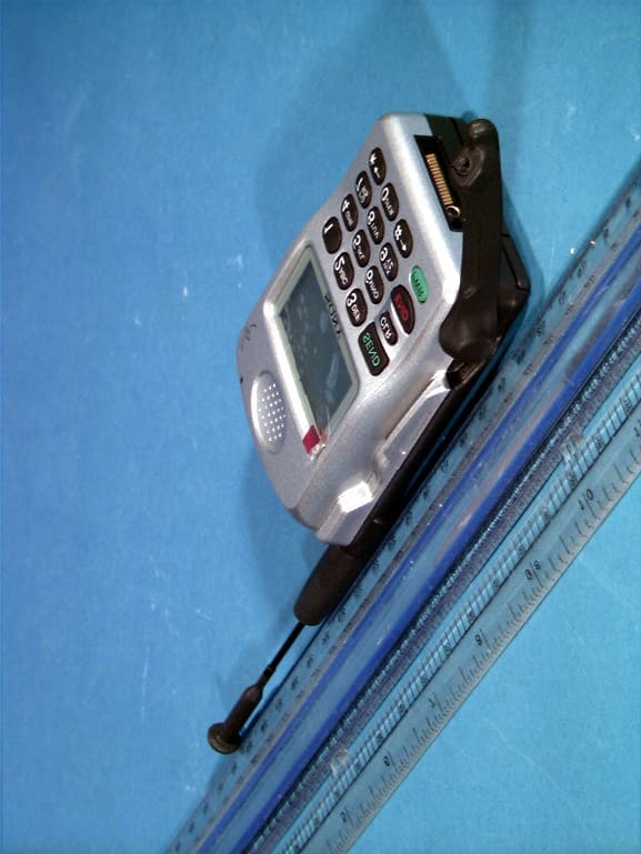
L5ACMZ200DM2
Apr 18, 1999DUAL MODE PORTABLE CELLULAR PHONE (AMPS/CDMA)
Equipment Class
TNE - Licensed Non-Broadcast Transmitter Held to Ear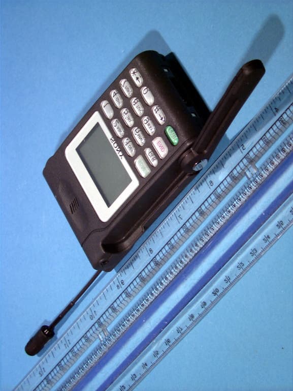
L5ACMZS300
Mar 17, 1999Single-Band PCS CDMA Phone
Equipment Class
PCE - PCS Licensed Transmitter held to ear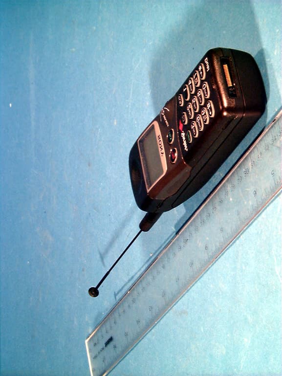
L5ACMSB2
Jan 11, 1999Single-Band PCS CDMA Phone
Equipment Class
PCE - PCS Licensed Transmitter held to ear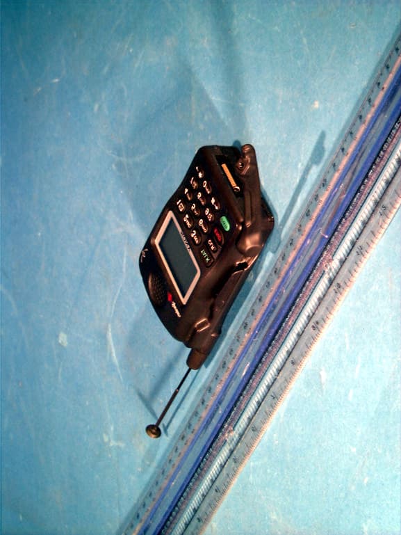
L5ACMZ100SB2
Dec 06, 1998PCE - PCS Licensed Transmitter held to ear
Equipment Class
PCE - PCS Licensed Transmitter held to ear