LE2GC43DIGITAL WIRELESS SURVEILLANCE SYSTEM
JSW Pacific Corporation
Click to zoom
Application Details
- Equipment Class
- DSS - Part 15 Spread Spectrum Transmitter
- Date of Grant
- Jun 05, 2012
- Application Purpose
- Original Equipment
- Date of Application
- Jun 05, 2012
- Equipment Note
- DIGITAL WIRELESS SURVEILLANCE SYSTEM
- Frequency Range
- 2414.25000000 - 2461.50000000
- Company
- JSW Pacific Corporation
- Country
- Taiwan
Documents & Files
Document Text
Text extracted from the exhibit documents filed with the FCC. Open a document above to read the original.
Users Manual
Digital Wireless Surveillance System User’s Guide 1 ˖̂́̇˸́̇̆ʳ ˪˻˴̇ϗ̆ʳ ̃́˶˿̈˷˸˷ʳˁˁˁˁˁˁˁˁˁˁˁˁˁˁˁˁˁˁˁˁˁˁˁˁˁˁˁˁˁˁˁˁˁˁˁˁˁˁˁˁˁˁˁˁˁˁˁˁˁˁˁˁˁˁˁˁˁˁˁˁˁˁˁʳˆʳ ˪˻˴̇ʳ ̊̈˴̅˷˼˴́ʳ˖˴́ʳ˗ ̂ʳ ̇̂̅ʳˬ̂̈ˁˁˁˁˁˁˁˁˁˁˁˁˁˁˁˁˁˁˁˁˁˁˁˁˁˁˁˁˁˁˁˁˁˁˁˁˁʳˇʳ Using This Manual..............................................................................4 ̊˸̇̇˼́˺ʳ˦̇˴̅̇˸˷ʳˁˁˁˁˁˁˁˁˁˁˁˁˁˁˁˁˁˁˁˁˁˁˁˁˁˁˁˁˁˁˁˁˁˁˁˁˁˁˁˁˁˁˁˁˁˁˁˁˁˁˁˁˁˁˁˁˁˁˁˁˁˁˁˁʳˈʳ Getting to Know the Receiver........................................................5 5 Getting to Know the Camera .........................................................5 What the lights mean.................................................................5 Setting Up the Equipment ..............................................................6 Power Up the Receiver ..............................................................6 Mount the Camera Stand .........................................................6 Attach the camera.......................................................................7 Setting Up Your System ...................................................................8 Verify Receiver and Cameras are Paired.....................................8 Camera Setup ..............................................................................8 System Setup ................................................................................8 Recording setup...........................................................................8 ̊̈˴̅˷˼˴́ʳ˦̂˹̇̊˴̅˸ʳˢ̃˸̅˴̇˼̂́ʳˢ̉˸̅̉˼˸̊ʳˁˁˁˁˁˁˁˁˁˁˁˁˁˁˁˁˁˁˁˁˁˁˁʳˌʳ What the icons mean .............................................................. 10 ̊̈˴̅˷˼˴́ʳ˦̌̆̇˸̀ʳ˦˶̅˸˸́ʳ˗˸̆˶̅˼̃̇˼̂́̆ˁˁˁˁˁˁˁˁˁˁˁˁˁˁˁˁˁˁˁˁˁˁˁˁˁʳ˄˅ʳ Guardian Settings Screen............................................................. 12 Camera Setup Screen.............................................................. 14 Recorder Setup Screen ........................................................... 17 Network Setup Screen ............................................................ 19 Alarm Setup Screen ................................................................. 22 System Setup Screen............................................................... 25 Save to SD ................................................................................... 29 System Upgrade ....................................................................... 30 Default .......................................................................................... 30 Quick Tips........................................................................................... 31 Other Stuff ......................................................................................... 31 ˨̆˼́˺ʳˬ̂̈̅ʳ˦̌̆̇˸̀ʳˁˁˁˁˁˁˁˁˁˁˁˁˁˁˁˁˁˁˁˁˁˁˁˁˁˁˁˁˁˁˁˁˁˁˁˁˁˁˁˁˁˁˁˁˁˁˁˁˁˁˁˁˁˁˁˁʳˆ˅ʳ Playing Back Recorded Video ..................................................... 32 Adding New Cameras .................................................................... 32 Some things to know about pairing cameras:............... 33 Pair Camera................................................................................. 33 Managing Your Files....................................................................... 34 Setting your recordings to delete ...................................... 34 ˠ˴˼́̇˴˼́˼́˺ʳˬ̂̈̅ʳ˦̌̆̇˸̀ʳˁˁˁˁˁˁˁˁˁˁˁˁˁˁˁˁˁˁˁˁˁˁˁˁˁˁˁˁˁˁˁˁˁˁˁˁˁˁˁˁˁˁˁˁˁʳˆˈʳ ˦̂˿̉˼́˺ʳˣ̅̂˵˿˸̀̆ˁˁˁˁˁˁˁˁˁˁˁˁ ˁˁˁˁˁˁˁˁˁˁˁˁˁˁˁˁˁˁˁˁˁˁˁˁˁˁˁˁˁˁˁˁˁˁˁˁˁˁˁˁˁˁˁˁˁˁˁʳˆˉʳ ˟ ̆ ̊˔˟ ̃˧ ̃ ̆˦ʳˁˁˁˁˁˁˁˁˁˁˁˁˁˁˁˁˁˁˁˁˁˁˁˁˁˁˁˁˁˁˁˁˁˁˁˁˁˁˁ ˁˁˁˁˁˁˁˁˁˁˁˁˁˁˁˁˁˁˁˁˁˁˁˁˁˁˁˁˁˁʳˆˋʳ ʇ ʇ ʇ ʇ Genuine Uniden software will NEVER install Spyware, Adware, or other malicious files along with the program, nor does it ever attempt to contact any web sites. This software does not incorporate any Hardware Locking or other intrusive licensing schemes. This software is distributed AS-IS and offers no warranty whatsoever. You install this software at your own risk. Uniden assumes no responsibility or liability for any negative effects of the software’s use, mis-use, installation, uninstallation, etc. Copyright 2011. All rights allowed by law are hereby reserved. ˪˻˴̇ϗ̆ʳ ̃́˶˿̈˷˸˷ʳ You should have the following items: G4 Receiver and Base GC43 Camera (2) AC Adapter (3) Antenna (2) ̃˹ʳ˴́̌ʳ˼̇˸̀̆ʳ˴̅˸ʳ̀˼̆̆˼́˺ʳ̂̅ʳ˷˴̀˴˺˸˷ʿʳ˶̂́̇˴˶̇ʳ̂̈̅ʳ˖̈̆̇̂̀˸̅ʳ˖˴̅˸ʳ˟˼́˸ʳ˼̀̀˸˷˼˴̇˸˿̌ˁʳ ˡ˸̉˸̅ʳ̈̆˸ʳ˷˴̀˴˺˸˷ʳ̃̅ ̂˷̈˶̇̆ʴʳ 3 ˨̆˼́˺ʳ˧˻˼̆ʳˠ˴́̈˴˿ʳ This manual is set up in six main sections: ʇ ʇ ʇ ʇ ʇ ʇ Getting Started. This section describes your hardware and how to physically set it up. You will find Operations Overview. This section lists basic operations in an abbreviated format. It references screen details in the third section. Screen Descriptions. Here you will find detailed descriptions of each screen and how it is used. PC Access. This section tells you how to hook up your surveillance system to your PC and access it from a separate location Maintenance Troubleshooting Use the ___ section for an overview of setup procedures. When you are familiar with the screen setup, you can refer to this section 4 ̊˸̇̇˼́˺ʳ˦̇˴̅̇˸˷ʳ ̊˸̇̇˼́˺ʳ̇̂ʳ˞́̂̊ʳ̇˻˸ʳ˥˸˶˸˼̉˸̅ʳ˴́˷ʳ˖˴̀˸̅˴̆ʳ ˥˸˶˸˼̉˸̅ʳ˦̇˴́˷ʳ ʻ˵˴˶˾˂̆˼˷˸ʼʳ Receiver Power Power Dock On/Off Data Cable Connection SD slot AC Power Connection AC Power Pull-Out Connection Stand Front view Back view Power status Link status Light sensor l ˪˻˴̇ʳ̇˻˸ʳ˿˼˺˻̇̆ʳʳ LightStateWhat it means OnThe camera is on. Power 5 OffThe camera is off. status FlashingThe camera is in pairing mode. OrangeThe camera is connected to the receiver. Link status OffThe camera is in standby. ˦˸̇̇˼́˺ʳ˨̃ʳ̇˻˸ʳ ̆̄̈˼̃̀˸́̇ʳ ˦˸̇ʳ˨̃ʳ̇˻˸ʳ˥˸˶˸˼̉˸̅ʳ 1. If you are using the receiver as a stand-alone unit, flip out the stand on the back of the receiver and connect an AC adapter to the power input on the side of the receiver. If you are using the receiver in the base, insert the receiver into the base and connect an AC adapter to the input on the back of the base. 2. Connect the other end of the adapter to a 120 volt AC (standard indoor) power outlet. 3. Press the ʳˣˢ˪ ̆˥ button on t…
Text truncated - open the document above for the full version.
Cover Letter(s)
JSW Pacific Corporation Federal Communications Commission Authorization and Evaluation Division Confidentiality Request regarding application for certification of FCC ID: LE2GC43 Pursuant to Sections 0.457 and 0.459 of the Commission’s Rules, we hereby request confidential treatment of information accompanying this application as outlined below: Exhibit Type File Name Schematics Block Diagram Operational Description LE2GC43_SCH.pdf LE2GC43_BlockDiagram.pdf LE2GC43_CircuitDescription.pdf The above materials contain trade secrets and proprietary information not customarily released to the public. The public disclosure of these materials may be harmful to the applicant and provide unjustified benefits to its competitors. The applicant understands that pursuant to Section 0.457 of the Rules, disclosure of this application and all accompanying documentation will not be made before the date of the Grant for this application. Sincerely, ---------------------------- Min Chen / vice president
Cover Letter(s)
JSW Pacific Corporation FCC ID: LE2G C43 POWER OF ATTORNEY May 15, 2012 Federal Communications Commission Authorization and Evaluation Division 7435 Oakland Mills Road Columbia, MD 21046 To Whom It May Concern: We, the undersigned, hereby authorize Waltek Services (ShenZhen) Co., Ltd. (Philo Zhong) on our behalf, to apply to the Federal Communications Commission on our equipment. Any and all acts carried out by Waltek Services (ShenZhen) Co., Ltd. (Philo Zhong) on our behalf shall have the same effect as acts of our own. This authorization expires on May 14, 2013. This is to advise that we are in full compliance with the Anti-Drug Abuse Act. We, JSW Pacific Corporation, are not subject to a denial of federal benefits pursuant to Section 5301 of the Anti-Drug Act of 1988, 21 USC853a, and no party to the application is subject to a denial of federal benefits pursuant to that section. Sincerely, JSW Pacific Corporation ------------------------------- Min Chen / Vice president
Cover Letter(s)
JSW Pacific Corporation FCC ID:LE2G4 Model:G4 FCC ID:LE2GC43 Model:GC43 May 25,2012 Federal Communications Commission Authorization and Evaluation Division 7435 Oakland Mills Road Columbia, MD 21046 To Whom It May Concern: Model G4 is a monitor as a receiver, and model GC43 is a camera as a transmitter. They communicate with each other after they are paired by pressing the link button. Power on the camera and monitor separately, press the link button of camera, then press the camera setup option of monitor, the monitor will scan and search the valid camera id, select a camera id and press pairing. After several seconds, the light of link status of camera changes to orange, the camera is connected to the receiver now and they can communicate with each other. The user manual describes how to link. As requirements of FCC and IC rules, the model G4 and GC43 have to certify separately. They use the same RF module. Sincerely yours, Min Chen/Vice President JSW Pacific Corporation
External Photos
2.1 Product View 2.2 EUT – Appearance View
ID Label/Location Info
Page: 52 of 52 JSW Pacific Corporation FCC ID: LE2GC43 The results shown in this test report refer only to the sample(s) tested , This Test report cannot be reproduced, except in full, without prior written permission of the Company. WALTEK SERVICES Reference No.: WT12052781-D-S-F 17 FCC Label This device complies with Part 15 of the FCC Rules. Operation is subject to the following two conditions: (1) this device may not cause interference, and (2) this device must accept any interference, including interference that may cause undesired operation of the device. The Label must not be a stick-on paper. The Label on these products must be permanently affixed to the product and readily visible at the time of purchase and must last the expected lifetime of the equipment not be readily detachable. Proposed Label Location on EUT EUT Back View/ proposed FCC Label Location FCC ID: LE2GC43 This device complies with Part 15 of the FCC Rules. Operation is subject to the following two conditions: (1) this device may not cause harmful interference, and (2) this device must accept any interference received, including interference that may cause undesired operation.
ID Label/Location Info
FCC ID label sample for model:GC43 FCC ID: LE2GC43 This device complies with Part 15 of the FCC Rules. Operation is subject to the following two conditions: (1) this device may not cause harmful interference, and (2) this device must accept any interference received, including interference that may cause undesired operation.
Internal Photos
Page: 51 of 54 JSW Pacific Corporation FCC ID: LE2GC43 The results shown in this test report refer only to the sample(s) tested , This Test report cannot be reproduced, except in full, without prior written permission of the Company. WALTEK SERVICES Reference No.: WT12052781-D-S-F 16.3 EUT – Open View Battery placement Page: 52 of 54 JSW Pacific Corporation FCC ID: LE2GC43 The results shown in this test report refer only to the sample(s) tested , This Test report cannot be reproduced, except in full, without prior written permission of the Company. WALTEK SERVICES Reference No.: WT12052781-D-S-F 16.4 EUT – PCB View Page: 53 of 54 JSW Pacific Corporation FCC ID: LE2GC43 The results shown in this test report refer only to the sample(s) tested , This Test report cannot be reproduced, except in full, without prior written permission of the Company. WALTEK SERVICES Reference No.: WT12052781-D-S-F 16.5 RF Module - View
Operational Description
A7121 2.4GHz GFSK Transceiver Jan. 2011, Version 1.5AMICCOM Electronics Corporation Document Title 2.4GHz GFSK Transceiver with 3Mbps Revision History Rev. No.HistoryIssue DateRemark 1.0Transfer from AMIC. Modify ordering information.Nov. 9th, 2005Released 1.1 ReviseDimensions inPackage Information Apr. 28th, 2006Released 1.2AMICCOM LOGO Changed.Oct. 5 th , 2007Released 1.3Add final version logo, top marking info., reflow profile, Carry tape & reel dimensions Jun. 26 th , 2008Released 1.4Change English Company NameNov. 30, 2010 1.5Correct ordering information and remove A7122.Jan. 06, 2011 Important Notice: AMICCOM reserves the right to make changes to its products or to discontinue any integrated circuit product or service without notice. AMICCOM integrated circuit products are not designed, intended, authorized, or warranted to be suitable for use in life-support applications, devices or systems or other critical applications. Use of AMICCOM products in such applications is understood to be fully at the risk of the customer. A7121 2.4GHz GFSK Transceiver Jan. 2011, Version 1.51AMICCOM Electronics Corporation Typical Applications n Wireless digital audio n Wireless Mouse and Keyboard n 2.4GHz ISM Band Communication System nWireless game pad nWireless toy General Description A7121 is a monolithic CMOS integrated circuit for wireless applications in 2.4GHz ISM band. The device is provided in a 32-lead plastic QFN5X5 packaging and is designed as a complete GFSK transceiver up to 3Mbps/ 1Mbps data rate. The chip features a fully programmable frequency synthesizer with integrated VCO circuitry. Pin Configurations 1 2 3 4 5 6 7 8 910111213141516 24 23 22 21 20 19 18 17 3231302928272625 VT CPO VDD _ P LL XI XS YDR_PF BB_CLK MS1 RFO BP _ L IM2 BP _ L I M1 BP _BPF DDV_A RFI VDD _ VCO BP _ VCO RX_C LK R X _ S YN CD_TXEN TRXD T XD F _CLK RES TEN MS0 VDD _ D S P I _ TXD S P I _C LK SP I _CSBP _LPFS P I _ R XDB P _DSRSSI A7121 QFN Package Top View Important Notice: AMICCOM reserves the right to make changes to its products or to discontinue any integrated circuit product or service without notice. AMICCOM integrated circuit products are not designed, intended, authorized, or warranted to be suitable for use in life- support applications, devices or systems or other critical applications. Use of AMICCOM products in such applications is understood to be fully at the risk of the customer. A7121 2.4GHz GFSK Transceiver Jan. 2011, Version 1.52AMICCOM Electronics Corporation Block Diagram OSCILLATOR VCO MOD System Control Logic MODEM INTERFACE 4 5 7 8 1 6 3 2 16 15 14 13 1211 109 18 19 20 23 24 21 22 17 28 27262531 30 2932 PA AGC LNA 90 LPF DS LIMITE R RSSI BPF SPI P LL C R YS TAL RX_CLK R X _ S YN CD_TXEN TRXD TXD F _ C LK RESTEN MS0 BP _ L IM2 BP _ L I M1 BP _ VCO VDD _ VCO BP _BPF V DD_D S P I _ R XD S P I _ T XD S P I _C LKSP I _CS BP_LPF BP _DS RSSI M S1 BB_CLK YDR_PF XS XI VDD_PLL CPO VT ORF RFI DDV_A System Block Diagram A7121 2.4GHz GFSK Transceiver Jan. 2011, Version 1.53AMICCOM Electronics Corporation Specification(Ta=25°C, VDD=2.5V, data rate= 3Mbps, TX data without Gaussian shaping unless otherwise noted.) ParameterDescriptionMinimumTypicalMaximumUnit General Operating Temperature-4085 °C Supply Voltage2.252.52.75V RX Mode28mA TX Mode @0dBm output34mA TX Mode @-6dBm output24mA Synthesizer Mode10mA Standby Mode1.5mA Current Consumption Transceiver Circuit Sleep Mode 2 mA Phase Locked Loop X’TAL Settling Time5ms @1M Mode 1 4, 8, 12, 16, 20X’TAL Frequency @3M Mode 1 9,18 MHz VCO Operation Frequency2400~2484MHz PLL Settling Time @settle to 20KHz @ Loop BW = 30 KHz 150 ms Transmitter TX Power@ Maximum Power Setting04dBm Power Control Range6dB Adjacent Channel-20dBc Second Channel-20dBm In-band Spurious ≧Third Channel -40dBm 30MHz~1GHz-36 1GHz~12.75GHz-30 1.8GHz~ 1.9GHz-47 Out-band Spurious 2 (Operating Mode) 5.15GHz~ 5.3GHz-47 dBm @1M Mode250Frequency Deviation @3M Mode750 KHz TX Settling Time @ Loop BW = 30 KHz 30 ms Receiver @1M Mode-85Sensitivity @BER=0.001 @3M Mode-80 dBm @1M Mode2IF Frequency @3M Mode4.5 MHz Image Rejection20dB Maximum Input Power@RF input-20dBm 30MHz~1GHz-57Spurious Emission 2 1GHz~12.75GHz-47 dBm AGC Gain Control0, 5, 15, 20dB RSSI Range@RF input-95-55dBm RSSI Slope Accuracy@RF input= -70 and –80 dBm20% RX Settling Time @ Loop BW = 30 KHz 30 ms A7121 2.4GHz GFSK Transceiver Jan. 2011, Version 1.54AMICCOM Electronics Corporation Digital IO DC characteristics High Level Input Voltage (V IH )0.8*VDDVDDV Low Level Input Voltage (V IL )00.2*VDDV High Level Output Voltage (V OH )@I OH = -0.5mAVDD-0.4VDDV Low Level Output Voltage (V OL )@I OL = 0.5mA00.4V Note: 1. Data rate= 1Mbps @1M Mode, Data rate= 3Mbps @3M Mode. 2. With external RF filter that provides minimum 17dB of attenuation in the band: 30MHz ~ 2GHz and 3GHz ~12.75GHz. A7121 2.4GHz GFSK Transceiver Jan. 2011, Version 1.56AMICCOM Electronics Corporation Absolute Maximum Ratings ParameterWith respect toRatingUnit Supply voltage range (VDD)GND-0.3 ~ 5.0Vdc Other I/O pins rangeGND-0.3 ~ VDD+0.3Vdc Maximum input RF level0dBm Storage Temperature range-55 ~ 125 °C *Stresses above those listed under “Absolute Maximum Rating” may cause permanent damage to the device. These are stress ratings only; functional operation of the device at these or any other conditions above those indicated in the operational sections of this specification is not implied. Exposure to absolute-maximum-rated conditions for extended periods may affect device reliability. *Device is ESD sensitive. Use appropriate ESD precautions. *Device is Moisture Sensitivity Level III (MSL 3). A7121 2.4GHz GFSK Transceiver Jan. 2011, Version 1.57AMICCOM Electronics Corporation State Description 1. A7121 State: The state machine inside the chip controls the A7121 GFSK transceiver operation. During normal operation, the A7121 is in one of five states (i.e., SLEEP, STBY, RADIO, CAL, TEMP). The state diagram is shown in Figure 1 below. Figure 1: A7121 State Diagram The A71…
Text truncated - open the document above for the full version.
Operational Description
Hop e Technology Inc. HPC3 129 Preliminary Datasheet V ersion 0.1 2010/06/18 HPC 3129 preliminary datasheet Con fidential and proprietary I I Ho pe T echnology Inc. Do cument number: TBD. Date: 201 0.06.18 App lication Information This document is designed for datasheet of HPC3129 chipset, approved to be released to and used by customers. To obtain the most updated Application Notes and other useful information for your design, contact your local Hope sales office. Please also visit the Hope web site at www.hopemicro.com Copyright Notice This manual is copyrighted by Hope Technology Inc. Do not reproduce or transform the manual to any other format, or send/transmit any part of this documentation without the expressed written permission of Hope Technology Inc. Trademark Acknowledgment Hope Technology® Digital logo is registered trademark of Hope Technology Inc. Disclaimer This document provides technical information for the user. Hope Technology Inc. reserves the right to modify the information in this document as necessary. The customer should make sure that they have the most recent data sheet version. Hope Technology Inc. holds no responsibility for any errors that may appear in this document. Customers should take appropriate action to ensure their use of the products does not infringe upon any patents. Hope Technology Inc. respects valid patent rights of third parties and does not infringe upon or assist others to infringe upon such rights. Copyright © Hope Technology Inc., 2010-2015. All rights reserved. HPC 3129 preliminary datasheet Con fidential and proprietary - 1 - 1 Over view The HPC3129 is an integrated system-on-chip application processor, which is designed to provide a low power and high performance multimedia solution for wireless monitor and CE market, such as Baby Monitor and hand-held devices. The HPC3129 is based on H-CORE, including a 32bit RISC processor with the addition of dedicated SIMD accelerator. The HPC3129 provides the high quality on-chip audio codec features, including 24bit stereo DAC and 24bit stereo ADC. The HPC3129 integrates many widely used multimedia processing functions for a simple and quick system integration, which include AMR codec, MP3 codec, WMA decoder, AAC codec, AAC+ decoder, OGG decoder, JPEG codec, MPEG4 and H.263 codec, H.264 codec etc. The HPC3129 also integrates a wireless communication baseband controller, named as HMAC, which could transmit or receive serial data to or from RF module. HMAC can easily interface with many popular RF transceivers, such as A7121(AMICCOM ® ). H ECC, a wireless communication error correction controller, is also included, which consists of CRC generator, RS encoder and RS decoder. So the HPC3129 is preferred for wireless multimedia applications. A large variety of peripherals and interfaces such as CAMERA, LCD, I 2 C, I2S, SDRAM, NAND Flash, ATA, SD/MMC/T-Flash, UART, SPI, Keypad, etc. provide the maximum flexibility and efficiency for building application systems. Main features of the HPC3129 are as follows: n Architecture: based on H-CORE, including a 32bit RISC processor with the addition of dedicated 128-bit SIMD accelerator n 193-Pin BGA package n Input image resolution up to (4096x4096) pixels n Support asynchronous MPU interface(80 type) LCD, support synchronous RGB LCD, and support variable display window size and OSD up to 1024x1024 n Microphone input(single end) n High performance headphone driver n Stereo line input n H-CORE based software supports main stream audio formats, such as MP3, AAC, AAC+, AMR NB, AMR WB, WMA, SBC, OGG, APE n SIMD based video decoder software supports main stream video formats, such as MPEG2, MPEG4/H.263, VC1, REAL VIDEO with performance up to D1@30fps n SIMD based JPEG codec supports encoder size up to 128M and decoder size up to 128M pixels n SIMD based video encoder software supports MPEG4 format with performance up to D1@30fps n Hardware H.264 codec supports H.264 format with performance up to D1@30fps n Support 16 bit or 32 bit data bus SDRAM or SRAM n Support up to two NAND devices, support up to 20 bit ECC by hardware BCH ECC accelerator HPC 3129 preliminary datasheet Con fidential and proprietary - 2 - n Support ATA-PIO mode 4 and UDMA-4 n Support SD memory card physical layer specification 2.0 n HMAC controller easy to interface with many popular RF transceivers n Including hardware HECC controller for wireless front error correction to improve RF performance n Related Video DAC integrated on chip, support for TV OUT up to D1 resolution n 2-channel single-ended 10-bit Successive Approximation Register (SAR) analog-to-digital converter(ADC) n Support up to an 4x4 external key pad matrix n With RTC function n Providing programmable clock out n With a large variety of interfaces such as I2C, I2S, SPI, UART, PWM, GPIO etc. HPC 3129 preliminary datasheet Con fidential and proprietary - 3 - 2 App lications Baby Monitor Wireless Video Doorbell Home Security Wireless Surveillance System PMP Photo Frame PDA DVR GPS Navigator DSC/DV HPC 3129 preliminary datasheet Con fidential and proprietary - 4 - 3 Function block diagram H-CORE RISC PROCESSOR H-CORE SIMD ACCERALTOR H.264 CODEC RESET CONTROLLER RTC BCH AUDIO CODEC ADC AND DAC SRAM/ SDRAM IF AT A/NAND FLASH IF SD/MMC/ T-FLASH IF TV OUT T IMER DMA C ONTROLLER INTERRUPT C ONTROLLER BOOT CONTROL GPIO IIC UAR T SPI(2) HMAC CAMERA IF LCD IF KEYPAD WATCHDOG HECC HPC3129 PWM CLOCK IN AND PLL I2S JTAG CLK OUT ADC (2 CH) GPMI IPU FI GURE 3-1 HPC3129 function block diagram HPC 3129 preliminary datasheet Con fidential and proprietary - 5 - 4 Feature sets 4.1 General features n Architecture: based on H-CORE, including a 32bit RISC processor with the addition of dedicated SIMD accelerator n Embedded 32-bit RISC MCU with 32Kbyte instruction cache and 32Kbyte data cache to reach high performance and lower bus-loading occupation n 128-bit SIMD accelerator n On-chip crystal oscillator with frequency of 24MHz n On-chip crystal oscillator w…
Text truncated - open the document above for the full version.
Test Report
Page: 1 of 54 FCC TEST REPORT The results shown in this test report refer only to the sample(s) tested , This Test report cannot be reproduced, except in full, without prior written permission of the Company. WALTEK SERVICES Reference No.: WT12052781-D-S-F FCC ID : LE2GC43 Applicant : JSW Pacific Corporation Address : 3F-3, No 700, Chung-Zweng Road Chung Ho City, Taipei, Hsien, Taiwan Equipment Under Test (EUT) : Product Name : Digital Wireless Camera Model No. : GC43 Standards : FCC CFR47 Part 15 Section 15.247:2010 Date of Test : May 7, 2012 ~ May 13, 2012 Date of Issue : May 14, 2012 Test Engineer : Hunk yan / Engineer Reviewed By : Philo zhong / Manager Test Result : PASS Prepared By: Waltek Services (Shenzhen) Co., Ltd. 1/F, Fukangtai Building, West Baima Rd., Songgang Street, Baoan District, Shenzhen 518105, China Tel :+86-755-27553488 Fax:+86-755-27553868 Page: 2 of 54 JSW Pacific Corporation FCC ID: LE2GC43 The results shown in this test report refer only to the sample(s) tested , This Test report cannot be reproduced, except in full, without prior written permission of the Company. WALTEK SERVICES Reference No.: WT12052781-D-S-F 2 Test Summary Test Items Test Requirement Result Radiated Spurious Emissions (18MHz to 25GHz) 15.205(a) 15.109&15.209 15.247(d) PASS Conduct Emission 15.107&15.207 PASS 20dB Bandwidth 15.247(a)(1) PASS Maximum Peak Output Power 15.247(b)(1) PASS Frequency Separation 15.247(a)(1) PASS Number of Hopping Frequency 15.247(a)(1)(iii) PASS Dwell time 15.247(a)(1)(iii) PASS Maximum Permissible Exposure (Exposure of Humans to RF Fields) 1.1307(b)(1) PASS Page: 3 of 54 JSW Pacific Corporation FCC ID: LE2GC43 The results shown in this test report refer only to the sample(s) tested , This Test report cannot be reproduced, except in full, without prior written permission of the Company. WALTEK SERVICES Reference No.: WT12052781-D-S-F 3 Contents Page 1 COVER PAGE ........................................................................................................................................................ 1 2 TEST SUMMARY .................................................................................................................................................. 2 3 CONTENTS............................................................................................................................................................. 3 4 GENERAL INFORMATION ................................................................................................................................ 5 4.1 CLIENT INFORMATION........................................................................................................................................... 5 4.2 GENERAL DESCRIPTION OF E.U.T. ........................................................................................................................ 5 4.3 DETAILS OF E.U.T................................................................................................................................................. 5 4.4 DESCRIPTION OF SUPPORT UNITS.......................................................................................................................... 6 4.5 STANDARDS APPLICABLE FOR TESTING................................................................................................................ 6 4.6 TEST FACILITY...................................................................................................................................................... 6 4.7 TEST LOCATION.................................................................................................................................................... 6 5 EQUIPMENT USED DURING TEST .................................................................................................................. 7 6 CONDUCTED EMISSION .................................................................................................................................... 9 6.1 E.U.T. OPERATION................................................................................................................................................ 9 6.2 EUT SETUP......................................................................................................................................................... 10 6.3 CONDUCTED EMISSION TEST RESULT................................................................................................................. 10 6.4 PHOTOGRAPH – CONDUCTED EMISSION TEST SETUP.......................................................................................... 13 7 RADIATED SPURIOUS EMISSIONS ............................................................................................................... 14 7.1 EUT OPERATION :............................................................................................................................................... 14 7.2 MEASUREMENT UNCERTAINTY........................................................................................................................... 14 7.3 TEST SETUP......................................................................................................................................................... 15 7.4 SPECTRUM ANALYZER SETUP............................................................................................................................. 17 7.5 TEST PROCEDURE................................................................................................................................................ 18 7.6 CORRECTED AMPLITUDE & MARGIN CALCULATION........................................................................................... 18 7.7 SUMMARY OF TEST RESULTS.............................................................................................................................. 19 7.8 PHOTOGRAPH – RADIATION SPURIOUS EMISSION TEST SETUP..................................................................…
Text truncated - open the document above for the full version.
Test Setup Photos
Below 30 MHz 30 MHz-1GHz Above 1GHz 2.1 Photograph – Conducted Emission Test Setup
Contact Information
Applicant
Min Hui Chen(Vice President)
Test Firm
Waltek Services(Shenzhen) Co., Ltd.Philo zhong
Technical Specifications
| # | Rule Parts | Frequency Range | Power Output |
|---|---|---|---|
| 1 | 15C | 2.41 GHz - 2.46 GHz | 100.00 mW |
Other Applications from JSW Pacific Corporation
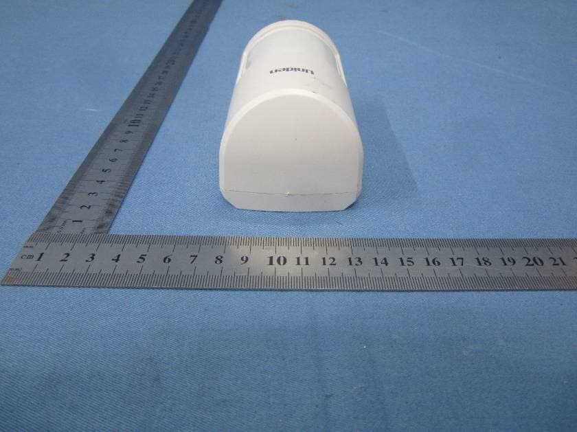
LE2PIR31
Nov 21, 2015Wireless portable / wall-mount area motion alert sensor
Equipment Class
DXX - Part 15 Low Power Communication Device Transmitter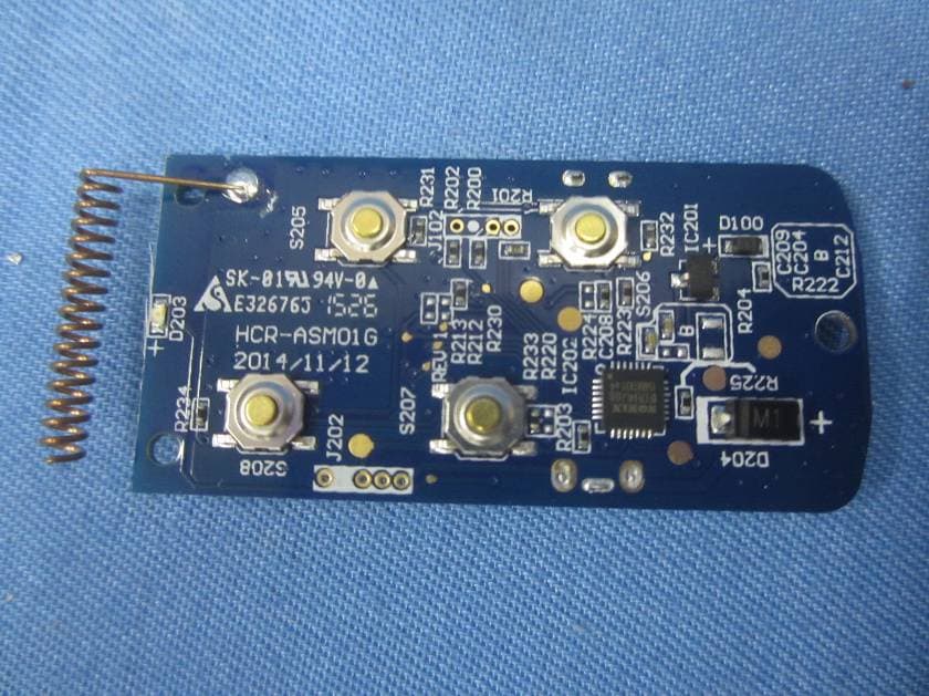
LE2RC41
Nov 21, 2015Wireless multi-functional panic remote controller
Equipment Class
DXX - Part 15 Low Power Communication Device Transmitter
LE2APPCAM26PTA
Jun 13, 2015720p PT WIFI Camera
Equipment Class
DTS - Digital Transmission System
LE2APPCAM25HDA
May 25, 2015720p WIFI Camera
Equipment Class
DTS - Digital Transmission System
LE2APPCAM24HD
May 24, 2015720p WIFI Camera
Equipment Class
DTS - Digital Transmission System