LE2RFB022.4GHz WIRELESS DIGITAL TRANSCEIVER MODULE
JSW Pacific Corporation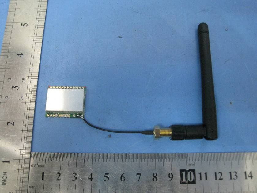
Click to zoom
Application Details
- Equipment Class
- DSS - Part 15 Spread Spectrum Transmitter
- Date of Grant
- Nov 27, 2011
- Application Purpose
- Original Equipment
- Date of Application
- Nov 27, 2011
- Equipment Note
- 2.4GHz WIRELESS DIGITAL TRANSCEIVER MODULE
- Frequency Range
- 2408.62500000 - 2474.87500000
- Company
- JSW Pacific Corporation
- Country
- Taiwan
Documents & Files
Document Text
Text extracted from the exhibit documents filed with the FCC. Open a document above to read the original.
Users Manual
FJK_RF_7121_A Wireless Digital Transceiver RFB02 A72121 17 dBm module specification MD7121-F07(-05) JSW Data Sheet CUSTOMER____________________ PRODUCT :2.4GHz Wireless digital Transceiver Module MODEL NO. RFB02 DATE: 2011-11-4 FJK_RF_7121_A Wireless Digital Transceiver RFB02 Rev. NO. History Issue Date Remark 0.0 0.1 0.2 0.3 Table of Contents 1. General Description ................................................ 3 2. Electrical specfication ............................................. 3 3. Interface ............................................................... 4 4. PA&LNA control state ................................................ 4 5. Application circuit ................................................... 5 6. Timing contril for passing CE/FCC .............................. 6 FJK_RF_7121_A Wireless Digital Transceiver RFB02 1. General Description The MD7121 module is designed for 2.4GHZ ISM band with 17dBm output power wireless applications using AMICCOM’s A7121 FSK/GFSK transceiver and A7700 RF Front End IC, This module features a fully programmable frequency synthesizer by SPI, The data rata is 1Mbps and 3Mbps. 2. Electrical speification Item Specification Remark Supply voltage 3.3V+/-0.1(V) Current consumption 15uA@Sleep mode (Sleep current includes power consumption of LDO) 1.5mA@Stand-by mode 11ma@Synthesizer Mode 130mA@Tx power =17dBm 36mA@ Rx mode typical Frequency 2408.625~2474.875MHz ISM band Tranmit output power 17dBm@Maximum Power Setting* 1 typical Rx sensitivity -93dBm(typical)@1M mode,Dev=250KHZ -88dBm(typical)@3M mode,Dev=750KHZ BER≤ 1E-3,FSK/GFSK Modulation FSK/GFSK Interface 20 pin1.27mm header PCB Dimension 29(L)*29(W)*0.8(H)mm 3 without antenna Operating temperature 0~50°C 3. Interface Pin NO. Pin name Comment Note 1 SPI_CS SPI chip select 2 SPI_CLK SPI clock 3 SPI_RXD SPI data input FJK_RF_7121_A Wireless Digital Transceiver RFB02 4 SPI_TXD SPI data output 5 SPI_CLK RX data sampling clock output 6 SPI_SYN RX sync signal output 7 SPI_TXEN TX mode:Modulation enable RX mode:Carrier detector 8 TRXD Input:TX data input Output:RX data output 9 TXD TX data input 10 F_CLK Clock for FIFO data 11 RESETN Chip reset 12 MS0 Transceiver operation mode selection input 13 MS1 Transceiver operation mode selection input 14 BB_CLK Clock output 15 VIN RF module supply voltage input 16 GND GND 17 FP_RDY Multi-function pin of FIFO packet R/W Complete or ready sinynal 18 GND GND 19 TXSW RF front end PA/LNA select 20 RXSW RF front end PA/LNA select 4. PA&LNA control state Control function RX ON TX ON TRX OFF Inhibit TXSW 1 0 1 0 RXSW 0 0 1 0 5. Pin Configuration and Mechanical Information FJK_RF_7121_A Wireless Digital Transceiver RFB02 6.Timing Control for passing CE/FCC: FJK_RF_7121_A Wireless Digital Transceiver RFB02 (1) FOR FIFO mode operation: If customers use FIFO Mode,the max.output power of MD7172-F07 should be set to 15dBm in order to pass CE/FCC A7121MSI A7121 CD_TXEN FP_RDY A7700_TXSW 60uS 4us 2us 2us (2) FOR FIFO mode operation: For passing CE/FCC regulation,customers can use the timing control below and set the output power to 17dBm. A7121MSI A7121 CD_TXEN A7700_TXSW 60uS 5us 2us 2us FJK_RF_7121_A Wireless Digital Transceiver RFB02 FCC NOTE: This device complies with Part 15 of the FCC Rules. Operation is subject to the following two conditions: (1) this device may not cause harmful interference, and (2) this device must accept any interference received, including interference that may cause undesired operation. The antenna used for this transmitter must be installed to provide a separation distance of at least 20 cm from all persons and must not be co-located or operated in conjunction with any other antenna or transmitter. The manufacturer is not responsible for any radio or TV interference caused by unauthorized modifications to this equipment. Such modifications could void the user's authority to operate the equipment. Note: This equipment contains module , FCC ID LE2RFB02, which qualifies as an UNLICENSED MODULAR TRANSMITTER per FCC Public Notice DA 00-1407. It has been tested and found to comply with Part 15.247 of the FCC Rules. This module has been designed for use by the JSW Pacific Corp. Required labeling. Any device incorporating this module must include an external, visible, permanent marking or label which states: ”Contains FCC ID: LE2RFB02.” Failure to comply with this requirement will void the user’s authority to operate any device that incorporates this module. This equipment complies with FCC radiation exposure limits set forth for uncontrolled equipment and meets the FCC radio frequency (RF) Exposure Guidelines in Supplement C to OET65. This equipment has very low levels of RF energy that it is deemed to comply without testing of specific absorption ratio(SAR).
Cover Letter(s)
JSW PACIFIC CORPORATION Federal Communications Commission Authorization and Evaluation Division Confidentiality Request regarding application for certification ofFCC ID: LE2RIB02. Pursuant to Sections 0.457 and 0.459 ofthe Commission's Rules, we hereby request confidential heatment of information accompanying this application as outlined below: Erhibit \pe File Name Schematics LE2RFB02_SCH.pdf Block Diagram LE2RFBo2_BlockDiagram.pdf Operational Description LE2RFB02_CircuitDescription.pdf The above materials contain tmde 6ecrc1s and proprietary information not customarily released to the public. The public disclosure ofthese materials may be harmful to the applicant and provide unjustified benefits to its competitors. The applicant und€rctands that pursuant to Section 0.457 ofthe Rules, disclosure ofthis application and all accompanying documentation will not be made before the date ofthe Grant for this aDDlication. Sincerely, Mh d*A Min Chin / Vice President
Cover Letter(s)
JSW Pacific Corporation 3F-3, No 700, Chung-Zweng Road Chung Ho City, Taipei, Hsien, Taiwan November 17, 2011 Subject: FCC ID: LE2RFB02 To Whom It May Concern: The following attestation address the requirements to support modular approval as required by the FCC. Rule Sections Description §15.212(a) This modular is a single modular transmitter consist of a completely self-contained radiofrequency transmitter device that is typically incorporated into another product, host or device. §15.212(a)(1)(i) The module has integral RF shielding to isolate it from surrounding equipment and the large environment in general §15.212(a)(1)(ii) All inputs are processed as data by the radio control element. The outside user has no direct control of transmit modulation. §15.212(a)(1)(iii) The radio front end contains a linear regulator to regulate device operation over voltage variations and to limit the output power under high voltage conditions. §15.212(a)(1)(iv) This module is validated with a dipole antenna. The reverse polarity SMA antenna connector is unique in the sense of complying with FCC §15.203, §15.204(b), §15.204(c). §15.212(a)(1)(v) The module was tested in a stand-alone configuration. It complies with the AC line conducted requirements found in FCC §15.207 requirements. §15.212(a)(1)(vi) An ID label is affixed to each unit at the time of manufacture. Information is also clearly presented in the user guide about labeling requirements for the final assembly. §15.212(a)(1)(vii) This module is compliant with FCC §15.247 rules. Installation and other requirements are presented in the user guide to allow the unit to be correctly installed. §15.212(a)(1)(viii) This module is compliant with the RF exposure requirements of FCC §15.247, §2.1091, §2.1093 Sincerely, JSW Pacific Corporation ------------------------- Min Chen / Vice President
Cover Letter(s)
.'$T PACIFIC CORPORATIOII POIIER OF ATTORNEY ECC ID: LE2RFB02 tgov€lb€- 10, 2011 Federal Cormunications Corunissiorr Authoriza!ion and Ewaluation Division 7435 Oakland Mllls Road Colunbia, MD 21046 To Whom lL l4av Concern: We, the unde.signed, hereby authorize Waltek Services (Shenzhen) Co., Ltd. (Philo Zhong) on our behalfr to appty to the rederat Conmunications CoflIission on our: equiptnent. Any and aII acts carried ou! by Waltek Sexvices (Shenzhen) Co., L!d. {Philo zhong) on our behalf shall have the same effect as acts of our own. This authorization expires on Noveob€r 9, 2012. This is to adwlse that $e are in futl conpliance r^rirh the Anti-Drug Abuse Act. We, itg PACrErC CORPOIIIIIOII, are not subject to a denial of federat benefits pursuant to Section 5301 of the Anti-Drug Act of 1988, 21 USC853a, and no party to the application is subject to a denial of federat benefits puisuan! to that 'AIl PACIPTC CORPORAIIOII w--/,q !4in Chen / Vice Pleaideat
External Photos
2.1 Product View 2.2 Module – Appearence View
ID Label/Location Info
Page:46 of 46 JSW Pacific Corporation FCC ID: LE2RFB02 WALTEK SERVICES Reference No.: WT11116044-D-E-F 17 FCC Label This device complies with Part 15 of the FCC Rules. Operation is subject to the following two conditions: (1) this device may not cause interference, and (2) this device must accept any interference, including interference that may cause undesired operation of the device. The Label must not be a stick-on paper. The Label on these products must be permanently affixed to the product and readily visible at the time of purchase and must last the expected lifetime of the equipment not be readily detachable. Proposed Label Location on Module Module Top View/ proposed FCC Label Location FCC ID: LE2RFB02
ID Label/Location Info
FCC ID Label Sample for Model: RFB02 FCC ID: LE2RFB02
Internal Photos
2.1 Module – Open View 2.2 Module - PCB View 2.3 Antenna View
Test Report
Page: 1 of 48 FCC TEST REPORT WALTEK SERVICES Reference No.: WT11116044-D-E-F FCC ID : LE2RFB02 Applicant : JSW Pacific Corporation Address : 3F-3, No 700, Chung-Zweng Road Chung Ho City, Taipei, Hsien, Taiwan Equipment Under Test (EUT) : Product Name : 2.4GHz Wireless Digital Transceiver Module Model No. : RFB02 Standards : FCC CFR47 Part 15 Section 15.247:2009 Date of Test : November 4 ~ November 8, 2011 Date of Issue : November 10, 2011 Test Engineer : Hunk yan / Engineer Reviewed By : Philo zhong / Manager Test Result : PASS Prepared By: Waltek Services (Shenzhen) Co., Ltd. 1/F, Fukangtai Building, West Baima Rd., Songgang Street, Baoan District, Shenzhen 518105, China Tel :+86-755-27553488 Fax:+86-755-27553868 The sample detailed above has been tested to the requirements of Council Directives ANSI C63.4:2003. The test results have been reviewed against the Directives above and found to meet their essential requirements. Page:2 of 48 JSW Pacific Corporation FCC ID: LE2RFB02 WALTEK SERVICES Reference No.: WT11116044-D-E-F 2 Test Summary Test Items Test Requirement Result Radiated Spurious Emissions (9kHz to 25GHz) 15.205(a) 15.209 15.247(d) PASS Conduct Emission 15.207 PASS 20dB Bandwidth 15.247(a)(1) PASS Maximum Peak Output Power 15.247(b)(1) PASS Frequency Separation 15.247(a)(1) PASS Number of Hopping Frequency 15.247(a)(1)(iii) PASS Dwell time 15.247(a)(1)(iii) PASS Maximum Permissible Exposure (Exposure of Humans to RF Fields) 1.1307(b)(1) PASS Page:3 of 48 JSW Pacific Corporation FCC ID: LE2RFB02 WALTEK SERVICES Reference No.: WT11116044-D-E-F 3 Contents 1 COVER PAGE........................................................................................................................................................ 1 2 TEST SUMMARY .................................................................................................................................................. 2 3 CONTENTS............................................................................................................................................................. 3 4 GENERAL INFORMATION ................................................................................................................................ 4 4.1 CLIENT INFORMATION........................................................................................................................................... 4 4.2 GENERAL DESCRIPTION OF E.U.T. ........................................................................................................................ 4 4.3 DETAILS OF E.U.T................................................................................................................................................. 4 4.4 DESCRIPTION OF SUPPORT UNITS.......................................................................................................................... 4 4.5 STANDARDS APPLICABLE FOR TESTING................................................................................................................ 4 4.6 TEST FACILITY...................................................................................................................................................... 5 4.7 TEST LOCATION.................................................................................................................................................... 5 5 EQUIPMENT USED DURING TEST .................................................................................................................. 6 6 CONDUCTED EMISSION .................................................................................................................................... 7 7 RADIATED SPURIOUS EMISSIONS ............................................................................................................... 12 8 RADIATED EMISSIONS WHICH FALL IN THE RESTRICTED BANDS................................................. 26 9 20 DB BANDWIDTH MEASUREMENT........................................................................................................... 31 10 MAXIMUM PEAK OUTPUT POWER ............................................................................................................. 33 11 HOPPING CHANNEL SEPARATION .............................................................................................................. 34 12 NUMBER OF HOPPING FREQUENCY .......................................................................................................... 37 13 DWELL TIME ...................................................................................................................................................... 38 14 ANTENNA REQUIREMENT ............................................................................................................................. 41 15 RF EXPOSURE .................................................................................................................................................... 42 16 PHOTOGRAPHS - CONSTRUCTIONAL DETAILS...................................................................................... 44 16.1 PRODUCT VIEW.............................................................................................................................................. 44 16.2 MODULE – APPEARENCE VIEW....................................................................................................................... 44 16.3 MODULE – OPEN VIEW................................................................................................................................... 45 16.4 MODULE - PCB VIEW..................................................................................................................................... 45 16.5 ANTENNA VIEW............................................................................................................................................. 46 17 FCC LABEL..........................................................................…
Text truncated - open the document above for the full version.
Test Setup Photos
Photograph – Radiation Spurious Emission Test Setup Below 1GHz Above 1GHz Photograph – Conducted Emission Test Setup
Contact Information
Applicant
Min Hui Chen(Vice President)
Test Firm
Waltek Services(Shenzhen) Co., Ltd.Philo zhong
Technical Specifications
| # | Rule Parts | Frequency Range | Power Output |
|---|---|---|---|
| 1 | 15C | 2.41 GHz - 2.47 GHz | 43.00 mW |
Other Applications from JSW Pacific Corporation
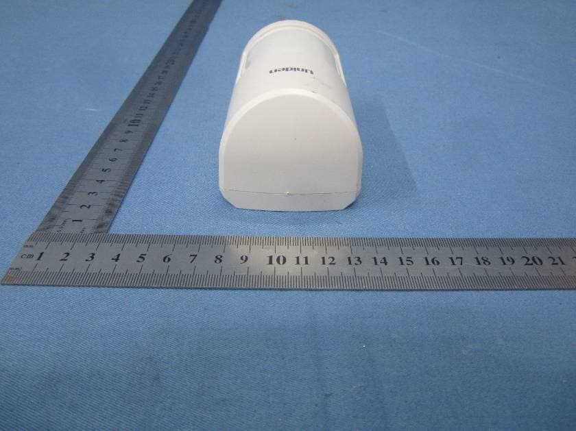
LE2PIR31
Nov 21, 2015Wireless portable / wall-mount area motion alert sensor
Equipment Class
DXX - Part 15 Low Power Communication Device Transmitter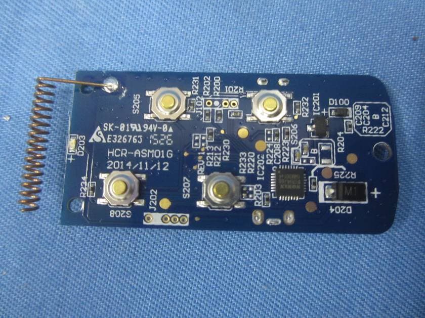
LE2RC41
Nov 21, 2015Wireless multi-functional panic remote controller
Equipment Class
DXX - Part 15 Low Power Communication Device Transmitter
LE2APPCAM26PTA
Jun 13, 2015720p PT WIFI Camera
Equipment Class
DTS - Digital Transmission System
LE2APPCAM25HDA
May 25, 2015720p WIFI Camera
Equipment Class
DTS - Digital Transmission System
LE2APPCAM24HD
May 24, 2015720p WIFI Camera
Equipment Class
DTS - Digital Transmission System