LLM101WL11000-2-EWireless PCMCIA LAN Card
Eumitcom Technology Inc.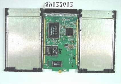
Click to zoom
Application Details
- Equipment Class
- DSS - Part 15 Spread Spectrum Transmitter
- Date of Grant
- Feb 13, 2001
- Application Purpose
- Original Equipment
- Date of Application
- Feb 13, 2001
- Equipment Note
- Wireless PCMCIA LAN Card
- Frequency Range
- 2412.00000000 - 2462.00000000
- Company
- Eumitcom Technology Inc.
- Country
- Taiwan
Documents & Files
Document Text
Text extracted from the exhibit documents filed with the FCC. Open a document above to read the original.
Users Manual
W W L L 1 1 1 1 0 0 0 0 0 0 Wireless LAN PCMCIA Adapter USER MANUAL Version 0.9.2, February 16, 2000 2 Federal Communications Commission Statement This device complies with FCC Rules Part 15. Operation is subject to the following two conditions: This device may not cause harmful interference. This device must accept any interference received, including interference that may cause undesired operation. This equipment has been tested and found to comply with the limits for a Class B digital device, pursuant to Part 15 of the FCC Rules. These limits are designed to provide reasonable protection against harmful interference in a residential installation. This equipment generates, uses and can radiate radio frequency energy. If this equipment is not installed and used in accordance with the manufacturer's instructions, it may cause harmful interference to radio communications. However, there is no guarantee that interference will not occur in a particular installation. If this equipment does cause harmful interference to radio or television reception, which can be determined by during the equipment off and on, the user is encouraged to try to correct the interference by one or more of the following measures: ! Reorient or relocate the receiving antenna. ! Increase the separation between the equipment and receiver. ! Connect the equipment to an outlet on a circuit different from that to which the receiver is connected. ! Consult the dealer or an experienced radio/TV technician for help. The use of shielded cables for connection of the monitor to the graphics card is required to assure compliance with FCC regulations. Changes or modifications to this unit not expressly approved by the party responsible for compliance could void the user's authority to operate this equipment. Manufacturer's Disclaimer Statement The information in this document is subject to change without notice and does not represent a commitment on the part of the vendor. No warranty or representation, either expressed or implied, is made with respect to the quality, accuracy or fitness for any particular purpose of this document. The manufacturer reserves the right to make changes to the content of this document and/or the products associated with it at any time without obligation to notify any person or organization of such changes. In no event will the manufacturer be liable for direct, indirect, special, incidental or consequential damages arising out of the use or inability to use this product or documentation, even if advised of the possibility of such damages. This document contains materials protected by copyright. All rights are reserved. No part of this manual may be reproduced or transmitted in any form, by any means or for any purpose without expressed written consent of its authors. Product names appearing in this document are mentioned for identification purchases only. All trademarks, product names or brand names appearing in this document are registered property of their respective owners. This device requires a radio license, unless it (including antenna ) is installed totally inside a building. (User must obtain this license from Industry Canada ). Printed in Taiwan 3 Contents Chapter 1 About the WL11000 PCMCIA Card ........................................................... 4 1-1 Features .............................................................................................................................................. 4 1-2 Applications ......................................................................................................................................... 4 1-3 Product Kit ........................................................................................................................................... 5 Chapter 2 Network Configuration and Planning ...................................................... 6 2-1 Network Topology................................................................................................................................ 6 2-2 Roaming .............................................................................................................................................. 8 Chapter 3 Adapter Installation and Configuration – Windows ® 98 ......................... 9 3-1 System Requirements ......................................................................................................................... 9 3-2 Inserting the Adapter ........................................................................................................................... 9 3-3 WL11000 Driver Installation -Windows ® 98 ....................................................................................... 10 3-4 Adapter Configuration – Windows ® 98............................................................................................... 13 3-5 Protocol Installation – Windows ® 98 .................................................................................................. 19 3-6 WL11000 Setup for Windows NT 4.0 ................................................................................................ 24 Chapter 4 Installing and Navigating the PRISM Configuration Utility .................. 28 4-1 PRISM Configuration Utility - Installation........................................................................................... 28 4-2 PRISM Configuration Utility- Navigation ............................................................................................ 31 Appendix A Troubleshooting................................................................................... 36 Appendix B Glossary................................................................................................ 38 4 Chapter 1 About the WL11000 PCMCIA Card The WL11000 IEEE 802.11 PCMCIA PC Card is compatible with any standard, notebook computer Type II or Type III PCMCIA slot. As a Plug-and-Play device, Windows 95/98 will automatically recognize the WL11000 PCMC…
Text truncated - open the document above for the full version.
Block Diagram
FLASH& VOLATILE RAM HFA3861A BBP HFA3783 QUAD IF HFA3841 MAC HFA3683A RF/IF CONV SAW BPF BPF HFA3983 RFPA BPF SCX CON SCX CON 44MHz Clock Eumitcom Technology Inc WL11000-2-E Block Diagram 1LO 2LO RG316 cable
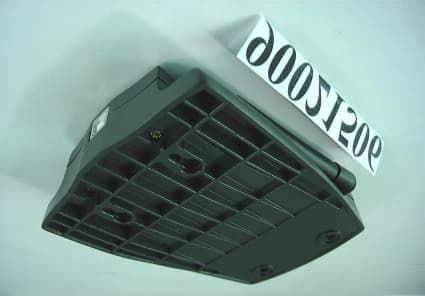
External Photos
Report No.: RF891226121Issued: Jan. 18, 2001 ANNEX PHOTOGRAPHS OF EUT Report No.: RF891226123Issued: Jan. 18, 2001 Report No.: RF891226124Issued: Jan. 18, 2001
ID Label/Location Info
WL11000-2-E FCC ID label: 1. The FCC ID label will paste in the bottom side of the product.( See figure below) MODEL : WL11000-2-E FCC ID: LLM101WL11000-2-E Canada ID: XXXXXXXXXXXXXX THIS DEVICE COMPLIES WITH PART 15 OF THE FCC RULES.OPERATIONS IS SUBJECT TO THE FOLLOWING TWO CONDITIONS (1) THIS DEVICE MAY NOT CAUSE HARMFUL INTERFERENCE AND(2) THIS DEVICE MUST ACCEPT ANY INTERFERENCE THAT MAY CAUSE UNDESIRED OPERATION. Eumitcom Technology Inc. Made in Taiwan 4 CM BOTTOM SIDE 6 CM
Internal Photos
Report No.: RF891226122Issued: Jan. 18, 2001 Report No.: RF891226125Issued: Jan. 18, 2001 Report No.: RF891226126Issued: Jan. 18, 2001
Operational Description
LLM101WL11000-2-E ADT No.89122612 Operational Description The transmitter of the EUT (Wireless LAN Card) is powered by host Desktop PC and connected with PC through PCI adapter which is a card used to transfer PCI to PCMCIA interface. The antenna is monopole and use MMCX antenna connector. Under normal use condition, the radiator of this device is easy to be located at least 20 cm far away from the body of the user. The other instruction, please have a look at the users manual.
Schematics
VS2* (NOT CONNECTED) PCMCIA 3.3 VOLT LOW TAGE KEYED GEN_MODE DIGITAL GROUND ANALOG GROUND 10 9 8 11 12 13 14 15 3 4 5 6 7 8 9 128K*8 SRAM 128K*8 SRAM 2 4 1 3 128K*8 SRAM 0 0 1 1 3 3 2 2 8 8 4 4 5 5 6 6 7 7 9 9 10 10 11 11 12 12 13 13 14 14 15 15 11 10 9 8 7 6 5 3 2 0 1 4 T9 8 9 10 11 12 13 14 15 0 1 2 3 4 5 6 7 8 10 9 11 12 13 14 15 16 17 0 1 2 4 5 6 3 7 3 1 0 4 NC NC NC NC NC NC NC 0123456789 101112131415 S_CLK S_DATA CSB PE1 LE_IF SCLK_RF_IF LEDI LE_RF SD_RF_IF PA_PE PE2 MD_RDY CCA CAL_EN TX_PE RX_PE RESET_BB* T/R_SW* SHEET 3 ANALOG/RF POWER PLAND DIGITAL POWER PLAND LOCATED CLOSE TO MAC AND SRAM DIGITAL GROUNDT10 ANALOG AND DIGITAL GROUND CLOSE TO CONNECTOR P1 NOTE:HRESET IS ACTIVE HIGH AND TIEO HIGH INTERNALLY IN THO HFA3841 0 CONNECT AGND TO DGND HERE SHEET 4 SHEET 2 SHEET 2 SHEET 2 SHEET 2,3,4 SHEET 2 SHEET 2 SHEET 2 SHEET 2 SHEET 3,4 SHEET 3 SHEET 4 SHEET 3,4 SHEET 3,4 SHEET 4 SHEET 3,4 SHEET 2 SHEET 2 SHEET 3 SHEET 2 SHEET 2 SHEET 2 SHEET 4 WL-SCH-WL11000-2-3V T2.0 Eumitcom Technology Inc. WL11000-2-E Custom 14Monday, January 08, 2001 Title SizeDocument NumberRev Date:Sheet of MOD * MA0(MWEH*) RAMCS* RAMCS * MOE* MOE* HD1 5 HD5 HD1 0 HD2 HD0 MOE* HD0HD2 HD11 HD12HD1 HD9 HD7 HD3 HD14 NVCS HD3 HD1 MWEL* HD9 HD13 MWEL* HD4 HD7 HD13HD14 HD6 HD11 HD10 HD6 HD8 HD4 MWEL * HD5 RAMCS HD8 HD1 2 HD15 NVCS* MEM CTRL [4..0] MEM CTRL [4..0] MA [17..0] HA[9..0] HA1HA5 HA1 HA4 HA9 HA2 HA6HA0HA7 HA8 HA7 HA4HA3 HA5 HA8 HA[9..0] HA6 HA3 HA0 HA9 HA[9..0] HA2 HA[9..0] MA17 MA4 MA16 MA15 MA[17..0] MA3 MA4 MA7 MA14 MA1 MA12 MA9 MA8 MA[0..17] MA11 MA9 MA2 MA5 MA13 MA16 MA5 MA7 MA13 MA17 MA12 MA3 MA10 MA11 MA11 MA15 MA0 MA14 MA13 MA12 MA10 MA4 MA16 MA6 MA[7..0] MA9 MA7 MA1 MA15 MA17 MA8 MA0 MA[7..0] MA3 MA10 MA14 MA8 MA8 MA9 MA0 MA5 MA7 MA1 MA6 MA5 MA12 MA2 MA16 MA1 MA6 MA6 MA3 MA4 MA2 MA2 MA15 MA10 MA11 MA14 MA13 MA[17..0] MEM CTRL [4..0] MEM CTRL [4..0] HD[15..0] HD[15..0] MEM CTRL [4..0] MD13 MD15 MD14 MD[15..0] MD15 MD9 MD10 MD14 MD[15..0] MD4 MD4 MD6 MD4 MD3 MD[0..7] MD7 MD1 MD0 MD11 MD3 MD8 MD0 MD6 MD[15..0] MD13 MD11 MD[15..0] MD7 MD1 MD2 MD9 MD4 MD5 MD10 MD14 MD0 MD6 MD3 MD10 MD2 MD2 MD12 MD12 MD1 MD0 MD6 MD2 MD12 MD[15..0] MD13 MD7 MD5 MD15 MD5 MD1 MD[15..0] MD[15..0] MD5 MD8 MD9 MD[15..0] MD8 MD7 MD3 MD11 HINPACK*HC2 HREG*HC3 HRESETHC0 HWE*HC8 HIREO*HC4 HIOWR*HC6 HSTSCHG*HC1 HSTSCHG*HC1 HIORD*HC7 HRESET*HC0 HWE*HC8 HWAIT*HC5 HCE2*HC10 HIREQ*HC4 HC10 HC[11..0] HC[11..0] HC11 HCE*HC9 HC9 HIOR*HC7 HIOWR*HC6 HCE2* HC[11..0] HREG*HC3HCE1* HOE* HCE1*HC11 HWAIT*HC5 HINPACK*HC2 P1-51-VCC2 P1-33-IOIS16*ASSEPIED OSI* +3.3V VCCS VCCS VCCS VH VCCS VCCS VCCS VCCS P1 PCMCIA 68X1 1 2 3 4 5 6 7 8 9 10 11 12 13 14 15 16 17 18 19 20 21 22 23 24 25 26 27 28 29 30 31 32 33 34 35 36 37 38 39 40 41 42 43 44 45 46 47 48 49 50 51 52 53 54 55 56 57 58 59 60 61 62 63 64 65 66 68 67 GND1 D3 D4 D5 D6 D7 CE1* A10 OE* A11 A9 A8 A13 A14 WE*/PGM* IREQ* VCC1 VPP1 A16 A15 A12 A7 A6 A5 A4 A3 A2 A1 A0 D0 D1 D2 IOIS16* GND2 GND3 CD1* D11 D12 D13 D14 D15 CE2* RFSH IORD* IOWR* A17 A18 A19 A20 A21 VCC2 VPP2 A22 A23 A24 A25 RFU RESET WAIT* INPACK* REG* SPKR STSCHG* D8 D9 D10 GND4 CD2* U2 AM29LV010B 10 11 5 4 12 1 31 2 3 13 14 15 16 17 18 19 20 30 32 7 29 28 27 26 25 23 22 21 9 6 8 24 A16 A15 A14 A13 A12 A11 A10 A9 A8 A7 A6 A5 A4 A3 A2 A1 A0 CE OE WE DO7 DO6 DO5 DO4 DO3 DO2 DO1 DO0 NC NC VCC VSS U4 1562LV1024LL 10 7 11 4 12 1 31 2 3 13 14 15 16 17 9 32 6 30 5 20 19 18 21 22 23 25 26 27 28 8 24 29 A16 A15 A14 A13 A12 A11 A10 A9 A8 A7 A6 A5 A4 A3 NC OE CD2 CD1 WE A0 A1 A2 I/O0 I/O1 I/O2 I/O3 I/O4 I/O5 I/O6 VCC GND I/O7 U1 1562LV1024LL 10 7 11 4 12 1 31 2 3 13 14 15 16 17 9 32 6 30 5 20 19 18 21 22 23 25 26 27 28 8 24 29 A16 A15 A14 A13 A12 A11 A10 A9 A8 A7 A6 A5 A4 A3 NC OE CD2 CD1 WE A0 A1 A2 I/O0 I/O1 I/O2 I/O3 I/O4 I/O5 I/O6 VCC GND I/O7 U3 HFA3841 72 73 74 75 76 77 78 79 80 81 84 85 86 87 88 89 90 91 92 61 60 59 62 10 31 30 32 29 65 8 70 71 54 55 56 57 58 68 69 7 35 34 33 63 64 21 22 23 15 27 26 28 43 12 11 51 50 49 48 47 46 45 44 101100996543296959412812712612512310610710810911011111211311711811221211161201191141021031636104 13374252678297115241425395366839812494193105171819204038 MA0 MA1 MA2 MA3 MA4 MA5 MA6 MA7 MA8 MA9 MA10 MA11 MA12 MA13 MA14 MA15 MA16 MA17 MA18 MD0 MD1 MD2 TRST TCLKIN PJ0 PJ1 PJ2 PJ3 PJ4 PJ5 MOE MWEC MD7 MD6 MD5 MD4 MD3 NVCS RAMCS PJ6 PK0 PK1 PK2 PK3 PK4 PK5 PK6 PK7 PL0 PL1 PL2 PL3 PL4 PL5 PL6 MD8 MD9 MD10 MD11 MD12 MD13 MD14 MD15 MD0MD1MD2MD3MD4MD5MD6MD7MD8MD9MD10MD11MD12MD13MD14MD15HA0HA1HA2HA3HA4HA5HA6HA7HA8HA9HCE1HCE2HOEHWEHIORHIOWRHIREOHREGHINPACKRESETHSTSCHGHWAIT VSS_CORE3VSS_CORE3 VSS_IO3VSS_IO3VSS_IO3VSS_IO3VSS_IO3VSS_IO3 VSS_-CORE3 VCC_CORE3VCC_CORE3VCC_CORE3VCC_CORE3 VCC_IO3VCC_IO3VCC_IO3VCC_IO3 PJ7 XTALO PL7 VCC_IO5 TXDTXCRXDRXC XTALI CLKOUT D5 LED 1 2 R3 470 1 2 R14 560 R72 1K 1 2 C81 0.1UF 1 2 C14 0.1UF 1 2 C31 0.1UF 1 2 + C9 10UF 1 2 + C102 10UF 1 2 L3 HMZ 201209T300Y-P 12 L17 HMZ 201209T300Y-P 12 + C34 10UF 1 2 C3 0.1UF 1 2 C2 0.1UF 1 2 C5 0.1UF 1 2 C10 0.1UF 1 2 C21 0.1UF 1 2 C20 0.1UF 1 2 C4 0.1UF 1 2 C8 0.1UF 1 2 C19 0.1UF 1 2 C7 0.1UF 12 C6 0.1UF 12 C1 0.1UF 12 R6 22K R78 22K R79 22K D1 MA25D10 R8 47K R7 47K R2647K R1 22K R2 22K R4 22K R12 22K R2147K R42 5.62K R18 5.62K R16 22K R947K R1747K R547K R1047K R1147K CCA MD_RDY SD_RF_IF S_DATA CSB PE1 LE_IF LE_RF SCLK_RF_IF PA_PE PE2 CAL_EN TX_PE RX_PE RESET_BB* T/R_SW* GEN_MODE GEN_MODE S_CLK TX_CLK RX_DATA T/R SW TX_DATA RADIO_PD 44MHz_REF RX_CLK A A B B C C D D E E 44 33 22 11 SMD_23X24 mil-PAD T8 T7 T6 T5 T4 T3 T2 T1 NC DIGITAL ANA LOG SHEET 1 SHEET 1 SHEET 3 SHEET 3 SHEET 3 SHEET 3 SHEET 3 SHEET 1,3 SHEET 1 SHEET 1 SHEET 1 SHEET 1 SHEET 1 SHEET 1 SHEET 1 SHEET 1 SHEET 1 SHEET 1 SHEET 4 SHEET 4 SHEET 4 SHEET 4 SHEET 3 SHEET 3 SHEET 3 SHEET 3 SHEET 3 SHEET 3 SHEET 3 NO POP WL-SCH-WL11000-2-3V T2.0 Eumitcom Technology Inc. WL11000-2 -E Custom 24Monday, January 08, 2001 Title SizeDocument NumberRev Date:Sheetof U5-21-IRDF U5-10-I IN+ COMPCAP2 U5-27-COMPRES2 U5-33-COMPCAP1 /ANT_SEL ANT_SEL RX_RF_AGC MCLK U5-41-BYP TEST0 TEST1 TEST2 TEST3 TEST4 TEST5 T…
Text truncated - open the document above for the full version.
Test Report
FCC ID: LLM101WL11000-2-E Report No.: RF89122612 1 Issued: Jan. 18, 2001 FCC TEST REPORT REPORT NO.: RF89122612 MODEL NO.: WL11000-2-E RECEIVED: December 26, 2000 TESTED: January 18, 2001 APPLICANT: Eumitcom Technology Inc. ADDRESS: 2F, No.2, Li Hsin Rd., Science-Based Industrial Park, Hsinchu, Taiwan, R.O.C. ISSUED BY: Advance Data Technology Corporation LAB LOCATION: 13-1, Lane 19, Wen Shan 3 rd St., Kweishan, Taoyuan Hsien, Taiwan, R.O.C. This test report consists of 68 pages in total. It may be duplicated completely for legal use with the approval of the applicant. It should not be reproduced except in full, without the written approval of our laboratory. The client should not use it to claim product endorsement by NVLAP or any U.S. government agencies. The test results in the report only apply to the tested sample. Accredited Laboratory FCC ID: LLM101WL11000-2-E Report No.: RF89122612 2 Issued: Jan. 18, 2001 Table of Contents 1CERTIFICATION ..................................................................................................... 4 2SUMMARY OF TEST RESULTS............................................................................ 5 3GENERAL INFORMATION ................................................................................... 6 3.1GENERAL DESCRIPTION OF EUT ............................................................ 6 3.2DESCRIPTION OF TEST MODES .............................................................. 6 3.3GENERAL DESCRIPTION OF APPLIED STANDARDS ............................. 7 3.4DESCRIPTION OF SUPPORT UNITS ........................................................ 7 4TEST PROCEDURES AND RESULTS .................................................................. 8 4.1CONDUCTED EMISSION MEASUREMENT............................................... 8 4.1.1LIMITS OF CONDUCTED EMISSION MEASUREMENT..................................................... 8 4.1.2TEST INSTRUMENTS ..........................................................................................................8 4.1.3TEST PROCEDURES...........................................................................................................9 4.1.4TEST SETUP ...................................................................................................................... 10 4.1.5TEST RESULTS.................................................................................................................. 11 4.2RADIATED EMISSION MEASUREMENT.................................................. 17 4.2.1LIMITS OF RADIATED EMISSION MEASUREMENT........................................................ 17 4.2.2TEST INSTRUMENTS ........................................................................................................ 18 4.2.3TEST PROCEDURES......................................................................................................... 19 4.2.4TEST SETUP ...................................................................................................................... 20 4.2.5TEST RESULTS.................................................................................................................. 21 4.36dB BANDWIDTH MEASUREMENT ......................................................... 25 4.3.1LIMITS OF 6dB BANDWIDTH MEASUREMENT ............................................................... 25 4.3.2TEST INSTRUMENTS ........................................................................................................ 25 4.3.3TEST PROCEDURE ........................................................................................................... 26 4.3.4TEST SETUP ...................................................................................................................... 26 4.3.5EUT OPERATING CONDITION.......................................................................................... 26 4.3.6TEST RESULTS.................................................................................................................. 27 4.4MAXIMUM PEAK OUTPUT POWER......................................................... 31 4.4.1LIMITS OF MAXIMUM PEAK OUTPUT POWER MEASUREMENT.................................. 31 4.4.2INSTRUMENTS .................................................................................................................. 31 4.4.3TEST PROCEDURES......................................................................................................... 32 4.4.4TEST SETUP ...................................................................................................................... 32 4.4.5EUT OPERATING CONDITION.......................................................................................... 32 4.4.6TEST RESULTS.................................................................................................................. 33 4.5POWER SPECTRAL DENSITY MEASUREMENT .................................... 34 4.5.1LIMITS OF POWER SPECTRAL DENSITY MEASUREMENT .......................................... 34 4.5.2TEST INSTRUMENTS ........................................................................................................ 34 4.5.3TEST PROCEDURE ........................................................................................................... 35 4.5.4TEST SETUP ...................................................................................................................... 35 4.5.5EUT OPERATING CONDITION.......................................................................................... 35 4.5.6TEST RESULTS.................................................................................................................. 36 4.6BAND EDGES MEASUREMENT .............................................................. 40 4.6.1LIMITS OF BAND EDGES MEASUREMENT..................................................................... 40 4.6.2TEST INSTRUMENTS ..........................................................................................…
Text truncated - open the document above for the full version.
Test Report
FCC ID: LLM101WL11000-2-E Report No.: RF89122612 45 Issued: Jan. 18, 2001 4.7 PROCESSING GAIN OF A DIRECT SEQUENCE SPREAD SPECTRUM MEASUREMENT(WORSE CASE) 4.7.1 LIMITS OF PROCESSING GAIN OF A DIRECT SEQUENCE SPREAD SPECTRUM MEASUREMENT Limit 4.7.2 TEST INSTRUMENTS & SUPPORT UNIT Description & ManufacturerModel No.Serial No. Hewlett Packard Spectrum Analyzer, 9kHz to 22GHz HP8593ES942848 Marconi Signal Generator, 10kHz to 2.7GHz 2031953426 Hewlett Packard Power Meter,HP438AS952633 Hewlett Packard Power Sensor, -20 to – 70dBm HP8481DSCD15369 Hewlett Packard Attenuator, 6dB to 10 dB HP8493ANA Hewlett Packard Step Attenuator, 1dB steps HP8494ANA Hewlett Packard Step Attenuator, 10dB ste ps HP8495DNA Hewlett Packard Power Splitter,HP11667B04390 Campaq Laptop Computer (Qty 2),Armada 1700NA FCC ID: LLM101WL11000-2-E Report No.: RF89122612 46 Issued: Jan. 18, 2001 4.7.3 METHOD OF MEASUREMENT The processing gain may be measured using the CW jamming margin method. Figure 1 shows the test configuration. The test consists of stepping a signal generator in 50 kHz increments across the passband of the system. At each point, the generator level required to produce the recommended Bit Error Rate (BER) is recorded. This level is jammer level. The output power of the transmitting unit is measured at the same point. The jammer to Signal (J/S) ratio is then calculated. Discard the worst 20% of the J/S data points. The lowest remaining J/S ratio is used when calculating the Process Gain. The reference PER is specified as 8%. The corresponding Es/No (signal to noise ratio per symbol) is 16.4 dB. The curve is attached as below. This value and the measured J/S ratio are used in the following equation to calculate the Process Gain (Gp) of the system. Where: (S/N) o : Signal to noise ratio for the chosen BER. Mj : Maximum jammer to Signal Ratio recorded at the detected BER. Gp = (S/N) o +Mj+Lsys FCC ID: LLM101WL11000-2-E Report No.: RF89122612 47 Issued: Jan. 18, 2001 Lsys : System losses . For the purpose of this processing gain calculation, we assume Lsys at its minimum value of 2 dB. Applicable Reference Documents. “HFA3861A Direct Sequence Spread Spectrum Baseband Processor” Harris Corporation Semiconductor Sector Preliminary Data Sheet, Melbourne FL, July 1999. “M-ary Orthogonal Keying BER Curve”. 4.7.4 TEST SETUP Transmitter HP11667B Power Splitter HP8493A HP8494A STEP ATTN 11dB (1dB steps) HP8495D HP8493A STEP ATTN 70dB (10dB steps) HP11667B Power Splitter HP8493A Receiver Matched Cables For the actual test configuration, please refer to the related Item – Photographs of the Test Configuration. Laptop Compaq Computer Armada 1700 PCMCIA CARD WL11000-1 10 dB MARCONI 2031 SIGNAL GENERATOR 6dB 10dB PCMCIA CARD Laptop Compaq Computer Armada 1700 PWR SENSOR HP 8481D Power meter HP 438A FCC ID: LLM101WL11000-2-E Report No.: RF89122612 48 Issued: Jan. 18, 2001 4.7.5 TEST PROCEDURES Obtain the simplex link shown. Perform all independent instrumentation calibrations prior to this procedure. Set operating power levels using fixed and variable attenuators in system to meet the following objectives: Signal Power at receiver approximately –60dBm (above thermal sensitivity such that thermal noise does not cause bit errors. Signal Power at power meter between –20 and –30dBm for optimal linearity. Use spectrum analyzer to monitor test. Ensure that CW Jammer generator RF output is disabled and measure the power at the power meter port using the power meter. This is the relative signal power, Sr. Disable Transmitter, and set CW Jammer generator RF output frequency equal to the carrier frequency and enable generator output. Set reference CW Jammer power level at power meter port 8.4dB below Sr (minimum J/S, or 10dB processing gain reference level). Note the power level setting on the generator, this is the reference CW Jammer power setting, Jr. Disable CW Jammer, re-establish link. PER test should be operating essentially error -free. Enable CW Jammer at the reference power level and verify that the PER test indicates a PER of less than 8%. Alternatively, adjust the CW Jammer level to that which causes 8% PER and verify that the S/J is less than 8.4dB. Repeat step 7 for uniform steps in frequency increments of 50 kHz across the receiver passband with the CW Jammer. In this case the receiver passband is +/- 8.5 MHz. The numerical data associated with the following radio channel is tabulated and presented for : CHANNEL 1 .................................................................................................. . Channel 6: 2437 MHz Channel 11 : 2462 MHz 4.7.6 EUT OPERATING CONDITION The software provided by client to set the EUT to transmit at lowest, middle and highest channel. FCC ID: LLM101WL11000-2-E Report No.: RF89122612 49 Issued: Jan. 18, 2001 4.7.7 TEST RESULTS EUT2.4GHz Wireless LAN Card Model WL11000-2-E Environmental Conditions Temperature:20°C Humidity:60% Te s t e d B ySteven Lu Although the theoretical processing gain is lower than 10 dB, but the CCK coding provides an extra coding gain of 2.2dB. 11Mbps CHANNEL 1 Processing Gain Gp = (S/N)。 。。 。+ Mj + Lsys Freq.Gp (S/N)。 。。 。 Mj = J/SLsysJammerLVL (GHz)(dB)(dB)(dB)(dB)(dBm)(dBm) 2.409511.316.4-7.12-47.1-0.7 2.4095511.416.4 -72-47-0.6 2.409611.416.4-72-47-0.6 2.4096511.416.4-72-47-0.6 2.409711.316.4-7.12-47.1-0.7 2.4097511.316.4-7.12-47.1-0.7 2.409811.116.4-7.32-47.3-0.9 2.4098511.116.4-7.32-47.30.9 2.40991116.4-7.42-47.4-1 2.409951116.4-7.42-47.4-1 2.4110.916.4-7.52-47.5-1.1 2.410051116.4-7.42-47.4-1 2.41011116.4-7.42-47.4-1 2.4101511.116.4-7.32-47.3-0.9 2.410211.216.4-7.22-47.2-0.8 2.4102511.316.4-7.12-47.1-0.7 2.410311.316.4-7.12-47.1-0.7 2.4103511.416.4-72-47-0.6 2.410411.316.4-7.12-47.1-0.7 2.4104511.316.4-7.12-47.1-0.7 2.410511.316.4-7.12-47.1-0.7 2.4105511.216.4-7.22-47.2-0.8 2.410611.216.4-7.22-47.2-0.8 2.4106511.316.4-7.12-47.1-0.7 2.410711.316.4-7.12-47.1-0.7 2.4107511.316.4-7.12-47.1-0.7 2.410811.416.4-72-47-0.6 2.4108511.516.4-6.92-46.9-0.5 2.4…
Text truncated - open the document above for the full version.
Test Setup Photos
FCC ID: LLM101WL11000-2-E Report No.: RF89122612 66 Issued: Jan. 18, 2001 5 PHOTOGRAPHS OF THE TEST CONFIGURATION CONDUCTED EMISSION TEST FCC ID: LLM101WL11000-2-E Report No.: RF89122612 67 Issued: Jan. 18, 2001 RADIATED EMISSION TEST
Contact Information
Applicant
Roger Wu(Vice President)
886 3 578-5717Fax: 886 3 578-5817
Test Firm
Bureau Veritas CPS (H.K.) Ltd. Taoyuan BranchTommy Wu
Technical Specifications
| # | Rule Parts | Frequency Range | Power Output |
|---|---|---|---|
| 1 | 15C | 2.41 GHz - 2.46 GHz | 32.00 mW |
Other Applications from Eumitcom Technology Inc.
LLM0102WN3501A
Mar 19, 2001Wireless USB Adapter
Equipment Class
DSS - Part 15 Spread Spectrum Transmitter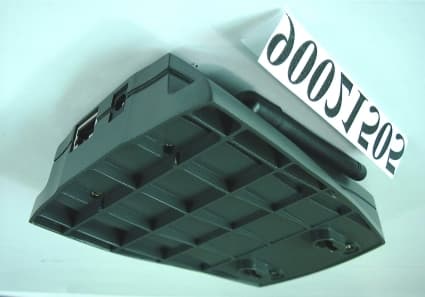
LLM0102WA3001A
Mar 19, 200111Mbps WLAN Access Point
Equipment Class
DSS - Part 15 Spread Spectrum Transmitter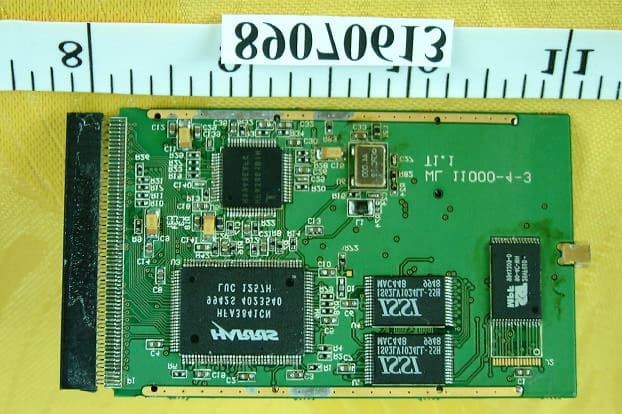
LLM007WL11000-2
Oct 30, 2000Wireless LAN Card
Equipment Class
DSS - Part 15 Spread Spectrum Transmitter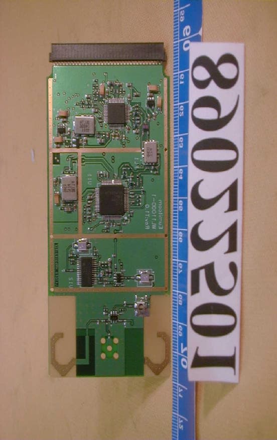
LLM002WL11000-1
May 18, 2000PCMCIA Card
Equipment Class
DSS - Part 15 Spread Spectrum Transmitter
LLM9908WL1000
Jan 11, 2000JBP - Part 15 Class B Computing Device Peripheral
Equipment Class
JBP - Part 15 Class B Computing Device Peripheral