M4Y-75011 M Wireless LAN USB Adapter
Z Com Inc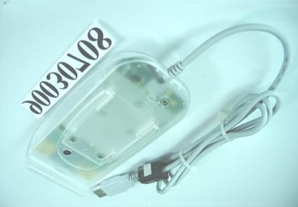
Click to zoom
Application Details
- Equipment Class
- DSS - Part 15 Spread Spectrum Transmitter
- Date of Grant
- Apr 26, 2001
- Application Purpose
- Original Equipment
- Date of Application
- Apr 26, 2001
- Equipment Note
- 11 M Wireless LAN USB Adapter
- Frequency Range
- 2412.00000000 - 2462.00000000
- Company
- Z Com Inc
- Country
- Taiwan
Documents & Files
Document Text
Text extracted from the exhibit documents filed with the FCC. Open a document above to read the original.
Users Manual
1 11Mbps Wireless LAN USB Adapter Quick Installation Guide Version 1.0.0 Network Configuration 11Mbps Wireless USB Adapter provides you the easiest, fastest, way to access your wireless and wired network. The Wireless USB Adapter utilizes the latest advancement of PC industry – USB technology, which allows you to install and use the card reader easier than ever before. 11Mbps Wireless USB Adapter can be operated in Ad-Hoc and Infrastructure network configurations. Ad-Hoc mode allows wireless stations to join a Basic Service Set (i.e., peer-to- peer mode, without access point). Infrastructure mode allows wireless clients to join an Extended Basic Service Set (i.e., connect to access point) Package Content 11Mbps Wireless USB Adapter x 1 Software Floppy Disk x 1 Quick Installation Guide x 1 11Mbpsp Wireless USB Adapter Installation under Windows 98/Windows 2000 1. Connect the 11Mbps Wireless USB Adapter to the USB port on your computer. The PC will auto-detect the Wireless USB Adapter and a Found New Hardware Wizard windows shows up. 2. Click on Next and insert the software floppy disk into the floppy drive. Specify the location where the driver is placed then click on Next to continue. 3. The PC will find the corresponding driver. Follow the on-screen instructions to install the 11Mbps Wireless USB Adapter. 4. Click Finish to complete the installation. Proceed to the next section to install the Wireless LAN utility for the Wireless LAN USB Adapter. Infrastructure Network Ad-hoc Network Wired Network Wireless Network Access Point 2 Installation of Wireless LAN Utility 1. From the Start menu, go to Run and type a:\setup.exe. 2. Follow the on-screen instructions to install the Wireless LAN Utility. 3. Upon completion, go to Program Files and run the Wireless LAN Utility, the utility interface will then appear and configuration can be made. Use of Wireless LAN Utility The 11Mbps Wireless LAN Utility provides the following items for you to configure the 11Mbps Wireless USB Adapter: Configuration: This item allows you to modify the configuration parameters for the 11Mbps Wireless USB Adapter such as Network Type, Channel, SSID, Tx Rate, Preamble Type, RTS/CTS Threshold and Fragmentation Threshold. After making changes on the configuration, click on the Modify button to make the changes take affect. 3 Status: This item shows the current information on the 11Mbps Wireless LAN USB Adapter such as MAC address, Channel, SSID, Status, Signal Strength and Link Quality. Counter: You may monitor wireless traffic on the network. 4 AP Browser: You may browser all the Access Points available on the network. Encryption: The encryption function enables you to encrypt and decrypt you wireless data, making your data more secure. To enable the WEP encryption, select the encryption type, either 64 bit or 128 bit, enter the WEP Keys in the Key field, choose the WEP Key to use and then click Modify to make the configuration take affect. Technical Support You can find the most recent software and user documentation on the supplier Web site. If you have difficulty resolving the problem while installing or using the 11Mbps Wireless USB Adapter, please contact the supplier for support. 5 FCC Information This device complies with Part 15 of the FCC Rules. Operation is subject to the following two conditions: (1) this device may not cause harmful interference, and (2) this device must accept any interference received; including interference that may cause undesired operation. Federal Communications Commission (FCC) Statement This Equipment has been tested and found to comply with the limits for a Class B digital device, pursuant to Part 15 of the FCC rules. These limits are designed to provide reasonable protection against harmful interference in a residential installation. This equipment generates, uses and can radiate radio frequency energy and, if not installed and used in accordance with the instructions, may cause harmful interference to radio communications. However, there is no guarantee that interference will not occur in a particular installation. If this equipment does cause harmful interference to radio or television reception, which can be determined by turning the equipment off and on, the user is encouraged to try to correct the interference by one or more of the following measures: - Reorient or relocate the receiving antenna. - Increase the separation between the equipment and receiver. - Connect the equipment into an outlet on a circuit different from that to which the receiver is connected. - Consult the dealer or an experienced radio/TV technician for help. 6 The Wireless LAN USB Adapter Specifications Model 11Mbps Wireless LAN USB Adapter USB Adapter Standard USB Interface Operating Channels 11 for N. America, 14 Japan, 13 Europe (ETSI), 2 Spain, 4 France Operating Frequency 2.412-2.462 GHz ( N. America FCC) 2.412-2.484 GHz (Japan TELEC) 2.412-2.472 GHz (Europe ETSI) 2.457-2.462 GHz (Spain) 2.457-2.472 GHz (France) Range 11M: 460 feet = 140m (In open environment) 5.5M: 656 feet = 200m 2M: 885 feet = 270m 1M: 1311 feet = 400m RF TechnologyDirect Sequence Spread Spectrum ModulationCCK(11Mps, 5.5Mbps) , DQPSK(2Mbps) , DBPSK(1Mbps) Voltage5V + 10% USB power available Power Consumption Tx power consumption: < 350mA Rx power consumption: < 250mA Sleep Mode: 17mA Output Power12 dBm Sensitivity @PER < 0.08 11Mbps < -83 dBm 5.5Mbps < -86dBm 2Mbps < -89dBm 1Mbps < -91dBm Data Rate1,2,5.5,11 Mbps Media Access ProtocolCSMA/CA, 802.11 Compliant Support OSWindows 98/2000/ME
External Photos
Report No.: RF900307081Issued: April 9, 2001 ANNEX 2 PHOTOGRAPHS OF EUT
Operational Description
FCC ID: M4Y-750 ADT No.90030708 Operational Description The transmitter of the EUT (11M Wireless LAN USB Adapter) is powered from PC and connected with notebook through RJ45 port. The antenna is Printed PCB Antenna, there is no antenna connector . Under normal use condition, the user has to keep at least 20cm separation distance between radiator and the body of the user. The other instruction, please have a look at the users manual. DSSS Information This device is Direct Sequence Spread Spectrum, the data is mixed by pseudorandom code which is an orthogonal code. The mixed data is digital modulated by BPSK and QPSK technique depends on the data rates. The CCK coding is applied for increasing the data rate, and also the processing gain will be increased. The bit rates are 1,2,5.5,11Mbps, the symbol rates are 1,1,1.375,1.375Mbps, the chip rates are always 11Mbps. So, the Chip/symbol is 11,11,8 and 8 respectively. Although is higher bit rate, the processing gain is lower than 10, but the CCK coding used in higher bit rate will provide 2.2dB coding gain.
Test Report
FCC ID: M4Y-750 Report No.: RF90030708 1 Issued: April 9, 2001 FCC TEST REPORT REPORT NO.: RF90030708 MODEL NO.: XI-750 RECEIVED: March 7, 2001 TESTED: April 3, 2001 APPLICANT: ZCOM,Inc. ADDRESS: 7F-2, No.9, Prosperity RD.I, Science-Based Industrial Park, Hsinchu, Taiwan, R.O.C. ISSUED BY: Advance Data Technology Corporation LAB LOCATION: 13-1, Lane 19, Wen Shan 3 rd St., Kweishan, Taoyuan Hsien, Taiwan, R.O.C. This test report consists of 48 pages in total. It may be duplicated completely for legal use with the approval of the applicant. It should not be reproduced except in full, without the written approval of our laboratory. The client should not use it to claim product endorsement by NVLAP or any U.S. government agencies. The test results in the report only apply to the tested sample. Accredited Laboratory FCC ID: M4Y-750 Report No.: RF90030708 2 Issued: April 9, 2001 Table of Contents 1CERTIFICATION .................................................................................................. 4 2SUMMARY OF TEST RESULTS......................................................................... 5 3GENERAL INFORMATION ................................................................................ 6 3.1GENERAL DESCRIPTION OF EUT ................................................................................ 6 3.2DESCRIPTION OF TEST MODES ................................................................................... 6 3.3GENERAL DESCRIPTION OF APPLIED STANDARDS ............................................... 7 3.4DESCRIPTION OF SUPPORT UNITS.............................................................................. 7 4TEST PROCEDURES AND TEST RESULTS .................................................... 8 4.1CONDUCTED EMISSION MEASUREMENT................................................................. 8 4.1.1LIMITS OF CONDUCTED EMISSION MEASUREMENT ...........................................................8 4.1.2TEST INSTRUMENTS ....................................................................................................................8 4.1.3TEST PROCEDURES ......................................................................................................................9 4.1.4TEST SETUP ..................................................................................................................................10 4.1.5TEST RESULTS .............................................................................................................................11 4.2RADIATED EMISSION MEASUREMENT ................................................................... 17 4.2.1LIMITS OF RADIATED EMISSION MEASUREMENT .............................................................17 4.2.2TEST INSTRUMENTS ..................................................................................................................18 4.2.3TEST PROCEDURES ....................................................................................................................19 4.2.4TEST SETUP ..................................................................................................................................20 4.2.5TEST RESULTS .............................................................................................................................21 4.36dB BANDWIDTH MEASUREMENT ........................................................................... 25 4.3.1LIMITS OF 6 D B BANDWIDTH MEASUREMENT.....................................................................25 4.3.2TEST INSTRUMENTS ..................................................................................................................25 4.3.3TEST PROCEDURE.......................................................................................................................26 4.3.4TEST SETUP ..................................................................................................................................26 4.3.5EUT OPERATING CONDITION...................................................................................................26 4.3.6TEST RESULTS .............................................................................................................................27 4.4MAXIMUM PEAK OUTPUT POWER........................................................................... 31 4.4.1LIMITS OF MAXIMUM PEAK OUTPUT POWER MEASUREMENT......................................31 4.4.2INSTRUMENTS.............................................................................................................................31 4.4.3TEST PROCEDURES ....................................................................................................................32 4.4.4TEST SETUP ..................................................................................................................................32 4.4.5EUT OPERATING CONDITION...................................................................................................32 4.4.6TEST RESULTS .............................................................................................................................33 4.5POWER SPECTRAL DENSITY MEASUREMENT ...................................................... 34 4.5.1LIMITS OF POWER SPECTRAL DENSITY MEASUREMENT ................................................34 4.5.2TEST INSTRUMENTS ..................................................................................................................34 4.5.3TEST PROCEDURE.......................................................................................................................35 FCC ID: M4Y-750 Report No.: RF90030708 3 Issued: April 9, 2001 4.5.4TEST SETUP ..................................................................................................................................35 4.5.5EUT OPERATING CONDITION...................................................................................................35 4.5.6TEST RESULTS .........…
Text truncated - open the document above for the full version.
Test Report
FCC ID: M4Y-750 Report No.: RF90030708 34 Issued: April 9, 2001 4.5 POWER SPECTRAL DENSITY MEASUREMENT 4.5.1 LIMITS OF POWER SPECTRAL DENSITY MEASUREMENT The Limit of Power Spectral Density Measurement is 8dBm. 4.5.2 TEST INSTRUMENTS Description & ManufacturerModel No.Serial No.Calibrated Until ROHDE & SCHWARZ TEST RECEIVER ESMI839379/002Aug. 04, 2001 HP ATTENUATOR8496B3247A18505Cal. on use HP PLOTTER7475A2641V27755N/A Notes: 1.The measurement uncertainty is less than +/- 2.6dB, which is calculated as per the NAMAS document NIS81. 2.The calibration interval of the above test instruments is 12 months. And the calibrations are traceable to NML/ROC and NIST/USA. FCC ID: M4Y-750 Report No.: RF90030708 35 Issued: April 9, 2001 4.5.3 TEST PROCEDURE The transmitter output was connected to the spectrum analyzer through an attenuator, the bandwidth of the fundamental frequency was measured with the spectrum analyzer using 3 kHz RBW and 30 kHz VBW, set sweep time=span/3kHz. The power spectral density was measured and recorded. The sweep time is allowed to be longer than span/3KHz for a full response of the mixer in the spectrum analyzer. 4.5.4 TEST SETUP For the actual test configuration, please refer to the related Item – Photographs of the Test Configuration. 4.5.5 EUT OPERATING CONDITION The software provided by client enabled the EUT to transmit and receive data at lowest, middle and highest channel frequencies individually. EUT SPECTRUM ANALYZER Attenuator FCC ID: M4Y-750 Report No.: RF90030708 36 Issued: April 9, 2001 4.5.6 TEST RESULTS EUT11M wireless LAN USB adapterModelXI-750 Environmental Conditions 20°C, 65%RHTe s t e d B ySteven Lu CHANNEL NUMBER CHANNEL FREQUENCY (MHz ) RF POWER LEVEL IN 3 KHz BW (dBm) MAXIMUM LIMIT (dBm) PASS/FAI L 12412-14.458PASS 62437-13.448PASS 112462-13.778PASS FCC ID: M4Y-750 Report No.: RF90030708 37 Issued: April 9, 2001 CH1 FCC ID: M4Y-750 Report No.: RF90030708 38 Issued: April 9, 2001 CH6 FCC ID: M4Y-750 Report No.: RF90030708 39 Issued: April 9, 2001 CH11 FCC ID: M4Y-750 Report No.: RF90030708 40 Issued: April 9, 2001 4.6 BAND EDGES MEASUREMENT 4.6.1 LIMITS OF BAND EDGES MEASUREMENT Below –20dB of the highest emission level of operating band (in 100KHz RB). 4.6.2 TEST INSTRUMENTS Description & ManufacturerModel No.Serial No.Calibrated Until ROHDE & SCHWARZ TEST RECEIVER ESMI 848926/005 846839/018 Dec 03, 2001 HP ATTENUATOR8496B3247A18505Cal. on use HP PLOTTER7475A2641V27755N/A Notes: 1.The measurement uncertainty is less than +/- 2.6dB, which is calculated as per the NAMAS document NIS81. 2.The calibration interval of the above test instruments is 12 months. And the calibrations are traceable to NML/ROC and NIST/USA. 4.6.3 TEST PROCEDURE The transmitter output was connected to the spectrum analyzer via a low lose cable. Set both RBW and VBW of spectrum analyzer to 100 kHz with suitable frequency span including 100 kHz bandwidth from band edge. The band edges was measured and recorded. FCC ID: M4Y-750 Report No.: RF90030708 41 Issued: April 9, 2001 4.6.4 EUT OPERATING CONDITION The software provided by client enabled the EUT to transmit and receive data at lowest, middle and highest channel frequencies individually. 4.6.5 TEST RESULTS The spectrum plots are attached below. D2 line indicates the highest level, D1 line indicates the 20dB offset below D2. It shows compliance with the requirement in part 15.247(C). FCC ID: M4Y-750 Report No.: RF90030708 42 Issued: April 9, 2001 4.6.6 NOTE ON BAND EDGE EMISSION The band edge emission plot on page 43 shows 46.14dB delta between carrier maximum power and local maximum emission in restrict band (2.484GHz). The emission of carrier strength list in table of page 24 is 98.4dBμV/m, so the maximum field strength in restrict band is 98.4-46.14=52.26 dBμV/m which is under 54 dBμV/m limit. FCC ID: M4Y-750 Report No.: RF90030708 43 Issued: April 9, 2001 FCC ID: M4Y-750 Report No.: RF90030708 44 Issued: April 9, 2001 FCC ID: M4Y-750 Report No.: RF90030708 45 Issued: April 9, 2001 4.7 ANTENNA REQUIREMENT 4.7.1 STANDARD APPLICABLE For intentional device, according to FCC 47 CFR Section 15.203, an intentional radiator shall be designed to ensure that no antenna other than that furnished by the responsible party shall be used with the device. And according to FCC 47 CFR Section 15.247 (b), if transmitting antennas of directional gain greater than 6dBi are used, the power shall be reduced by the amount in dB that the directional gain of the antenna exceeds 6dBi. 4.7.2 ANTENNA CONNECTED CONSTRUCTION The antenna used in this product is Printed PCB Antenna. There is no antenna connector. And the maximum Gain of this antenna is only -1dBi. FCC ID: M4Y-750 Report No.: RF90030708 46 Issued: April 9, 2001 5 PHOTOGRAPHS OF THE TEST CONFIGURATION CONDUCTED EMISSION TEST FCC ID: M4Y-750 Report No.: RF90030708 47 Issued: April 9, 2001 RADIATED EMISSION TEST FCC ID: M4Y-750 Report No.: RF90030708 48 Issued: April 9, 2001 6 INFORMATION ON THE TESTING LABORATORIES We, ADT Corp., were founded in 1988 to provide our best service in EMC and Safety consultation. Our laboratories are accredited by the following approval agencies according to ISO/IEC Guide 25 or EN 45001: USA FCC, NVLAP Germany TUV Rheinland Japan VCCI New Zealand RFS Norway NEMKO, DNV U.K. INCHCAPE R.O.C. BSMI Copies of accreditation certificates of our laboratories obtained from approval agencies can be downloaded from our web site: www.adt.com.tw/index.5/phtml. If you have any comments, please feel free to contact us at the following: Lin Kou EMC Lab: Tel: 886-2-26052180 Fax: 886-2-26052943 Hsin Chu EMC Lab: Tel: 886-35-935343 Fax: 886-35-935342 Lin Kou Safety Lab: Tel: 886-2-26093195 Fax: 886-2-26093184 Design Center: Tel: 886-2-26093195 Fax: 886-2-26093184 Email: [email protected] Web Site: www.adt.com.tw
Test Report
1 Processing Gain of Direct Sequence Spread Spectrum Product name: XI750 Wireless LAN USB Adapter Tested by: Zcom, Inc. Prepared by: Gilbert Tsai, Associate RF engineer TEL: (886)35789700 ext.113 FAX: (886)3636033 Email: [email protected] Date: April 13, 2001 FCC requirements: The processing gain of a direct sequence system shall be at least 10dB. The processing gain shall be determined from the ratio in dB of the signal-to- noise ratio with the system spreading code turned off to the signal-to-noise ratio with the system spreading code turned on, as measured at the demodulated output of the receiver. This document contains theoretical calculation and test setup, procedure, measurement data and report. Test equipment: R&S FSEM20 spectrum analyzer R&S SMIQ03B signal generator Giga-tronics 8541C universal power meter Hp8496B attenuator/110dB with 10dB step Hp8494B attenuator/11dB with 1dB step Hp11636BB power splitter Notebook/PC X2 Theoretical calculation: The Processing gain is related to be jamming margin as follows: Where BER reference is the reference bit error ratio with its corresponding, theoretical output signal to noise ratio per symbol, (S/N) output , (J/S) is the jamming margin(jamming signal power relative to desired signal power), and L sys is the system losses. 2 For 5.5Mbps and 11Mbps case: The HFA3861B direct sequence spread spectrum baseband processor use CCK modulation which is a form of M-ary Orthogonal Keying. The Probability of error for generalized M-ary orthogonal signaling using coherent demodulation is given by: The FER performance curve is derived by [1] as left graph: Therefore: Gp = (Es/No)o + (J/S) + Lsys =16.4 + 2.0 + (J/S) and, Gp = 18.4 + (J/S) must be greater than 10dB For the case of the HFA3861B, the bit rates are 1,2, 5.5 and 11Mbps. The corresponding symbol rates are 1, 1, 1.375 and 1.375 Msps. The chip rate is always 11Mcps, so the ratio of chip rate to symbol rate is 11:1 for the 1, 2Mbps and 8:1 for 5.5, 11Mbps rates. Since the symbol rate to bit rate is less than 10 for the higher rates, we supply the theoretical processing gain and coding are utilized. This is a reasonable in that they cannot be separated in the demodulation process. If a separable FEC coding scheme were used, we would not be comfortable making this assertion. As can be seen from the curve of figure 1, the Es/No is 16.4dB at the PER of 8%. It is well know that the Eb/No of BPSK is 9.6dB for 1e-5 BER, so therefore the coding gain of CCK over BPSK is 2.2dB. We add this to the processing gain of 9B to get 11.2dB overall processing gain for the CW jamming test. 15.51616.517 10 -2 10 -1 10 0 11 Mbps CCK in Thermal Noise Es/No (dB) 1000 byte Packet Error Rate 3 Taking the calculation above, if the (J/S)>-8.4dB then the equipment passes the CW jamming test. For 1 and 2Mbps case, the modulation is either DBPSK or DQPSK for 1 and 2Mbps. With differential coding, there is an error extension factor of 2 which comes from the fact that if one symbol is error, then the next will be demodulated in error too. Since its phase is dependant on the change of phase from symbol to symbol. In DBPSK, this result is a simple factor of two in BER. With DQPSK, the picture is a little muddied in that a symbol error may cause one or two bit errors since two bits are carried per symbol. From the book of Fig.7.2, Viterbi, A.J. Principles of Coherent Communications, Page 192 (New York; McGraw-Hill, 1996), the Eb/No of BPSK is 9.6dB. When operating DQPSK at 2Mbps, the Eb/No remains essentially the same, but the Es/No goes up by 3dB. So the (S/N)o is 12.6. Test procedure: Obtain the simplex link shown. Perform all independent instrumentation calibration prior to this procedure. Set operating levels using fixed and variable attenuator in system to meet the following objectives: 1. Signal Power at receiver is approximately –60dBm. 2. Signal Power at power meter between –20 and –30dBm. 3. Use spectrum analyzer to monitor test. 4. Ensure that CW jammer generator RF output is disabled and measure the power at the power meter port using Giga-tronics 8541C power meter. This is relative power, Sr. 5. Disable TX and set CW jammer output frequency equal to the carrier frequency and enable generator output. Set reference CW jammer power level at power meter port 8.4dB below Sr. 6. Disable CW jammer and re-establish Link. FER test should be essentially error free. 7. Enable the CW jammer at the reference power level and verify that FER at the reference power level and verify that FER test indicate less than 8%. 8. Alternatively, adjust the CW jammer level to that which causes 8% FER. 9. Repeat Step 7 for uniform steps in frequency increments of 50KHz across the receiver passband with the CW jammer. In this case, the receiver passband is ±8.5MHz Test setup: as shown at next page 4 Processing gain test result summary: Frequency channelFrequencyData rate (Mbps)Gp (dB) 12412MHz1110.6 62437MHz1110.6 112462MHz1110.6 12412MHz213.8 62437MHz213.8 112462MHz213.8 Reference [1]. Intersil processing gain test document (Attached file). Processing gain test setup
Test Report
ZCOM, Inc. XI750 Processing GainFilename: xi750PGforFCC.xls Freq. (MHz)Gp (dB)(S/N)o (dB)Mj = J/S (dB)Lsys (dB)Jammer (dBm)Lvl (dBm)FER 2403.5020.812.66.22-2-8.26.1 2403.5519.812.65.22-3-8.24.8 2403.6019.812.65.22-3-8.25.7 2403.6519.812.65.22-3-8.26.2 2403.7019.812.65.22-3-8.26.7 2403.7519.812.65.22-3-8.25.4 2403.8019.812.65.22-3-8.25.2 2403.8518.812.64.22-4-8.25.8 2403.9019.812.65.22-3-8.26.1 2403.9519.812.65.22-3-8.26.7 2404.0019.812.65.22-3-8.26.6 2404.0519.812.65.22-3-8.25.7 2404.1020.812.66.22-2-8.25.6 2404.1520.812.66.22-2-8.26.2 2404.2018.812.64.22-4-8.26.4 2404.2520.812.66.22-2-8.24.8 2404.3020.812.66.22-2-8.26.3 2404.3520.812.66.22-2-8.25.4 2404.4020.812.66.22-2-8.26.1 2404.4519.812.65.22-3-8.26.2 2404.5019.812.65.22-3-8.25.8 2404.5519.812.65.22-3-8.26.7 2404.6019.812.65.22-3-8.26.2 2404.6519.812.65.22-3-8.26.3 2404.7019.812.65.22-3-8.26.6 2404.7518.812.64.22-4-8.26.5 2404.8019.812.65.22-3-8.26.9 2404.8518.812.64.22-4-8.27.6 2404.9018.812.64.22-4-8.26.3 2404.9519.812.65.22-3-8.25.9 2405.0018.812.64.22-4-8.26.4 2405.0519.812.65.22-3-8.26.1 2405.1019.812.65.22-3-8.26.2 2405.1519.812.65.22-3-8.25.8 2405.2019.812.65.22-3-8.25.3 2405.2519.812.65.22-3-8.25.6 2405.3019.812.65.22-3-8.25.5 2405.3519.812.65.22-3-8.26.3 2405.4017.812.63.22-5-8.29.8 2405.4518.812.64.22-4-8.26.6 2405.5018.812.64.22-4-8.26.1 2405.5518.812.64.22-4-8.26.7 2405.6018.812.64.22-4-8.25.7 2405.6518.812.64.22-4-8.27.6 2405.7018.812.64.22-4-8.27.2 2405.7517.812.63.22-5-8.27.1 2405.8016.812.62.22-6-8.26.8 2405.8517.812.63.22-5-8.26.3 2405.9017.812.63.22-5-8.26.5 2405.9516.812.62.22-6-8.26.1 2406.0018.812.64.22-4-8.26.2 2406.0516.812.62.22-6-8.26.9 2406.1017.812.63.22-5-8.26.6 2406.1518.812.64.22-4-8.26.1 2406.2017.812.63.22-5-8.26.7 2Mbps Channel 1 Processing Gain Gp=(S/N)o+Mj+Lsys XI750PG_2M_CH11/42Date: 2001/4/13 ZCOM, Inc. XI750 Processing GainFilename: xi750PGforFCC.xls Freq. (MHz)Gp (dB)(S/N)o (dB)Mj = J/S (dB)Lsys (dB)Jammer (dBm)Lvl (dBm)FER 2Mbps Channel 1 Processing Gain Gp=(S/N)o+Mj+Lsys 2406.2520.812.66.22-2-8.26.6 2406.3019.812.65.22-3-8.26.3 2406.3521.812.67.22-1-8.26.8 2406.4022.812.68.220-8.26.1 2406.4522.812.68.220-8.26.7 2406.5022.812.68.220-8.26.4 2406.5522.812.68.220-8.24.8 2406.6020.812.66.22-2-8.25.6 2406.6518.812.64.22-4-8.26.3 2406.7018.812.64.22-4-8.26.7 2406.7517.812.63.22-5-8.26.2 2406.8017.812.63.22-5-8.26.8 2406.8515.812.61.22-7-8.26.3 2406.9015.812.61.22-7-8.25.9 2406.9514.812.60.22-8-8.26 2407.0015.812.61.22-7-8.25.7 2407.0513.812.6-0.82-9-8.27.9 2407.1015.812.61.22-7-8.26.4 2407.1515.812.61.22-7-8.24.8 2407.2015.812.61.22-7-8.26.9 2407.2514.812.60.22-8-8.25.4 2407.3014.812.60.22-8-8.26.5 2407.3515.812.61.22-7-8.27.6 2407.4016.812.62.22-6-8.27.1 2407.4512.812.6-1.82-10-8.26.7 2407.5012.812.6-1.82-10-8.25.6 2407.5514.812.60.22-8-8.27.4 2407.6015.812.61.22-7-8.26.8 2407.6515.812.61.22-7-8.26.3 2407.7012.812.6-1.82-10-8.25.9 2407.7515.812.61.22-7-8.26.2 2407.8014.812.60.22-8-8.27.1 2407.8514.812.60.22-8-8.27.3 2407.9014.812.60.22-8-8.27.4 2407.9514.812.60.22-8-8.26.8 2408.0015.812.61.22-7-8.25.8 2408.0513.812.6-0.82-9-8.26.7 2408.1013.812.6-0.82-9-8.26.6 2408.1513.812.6-0.82-9-8.26.9 2408.2012.812.6-1.82-10-8.27 2408.2514.812.60.22-8-8.27.6 2408.3014.812.60.22-8-8.26.3 2408.3514.812.60.22-8-8.25.2 2408.4015.812.61.22-7-8.25.4 2408.4513.812.6-0.82-9-8.24.6 2408.5015.812.61.22-7-8.25.6 2408.5515.812.61.22-7-8.27.4 2408.6014.812.60.22-8-8.26.8 2408.6516.812.62.22-6-8.26.3 2408.7013.812.6-0.82-9-8.25.9 2408.7513.812.6-0.82-9-8.26.2 2408.8010.812.6-3.82-12-8.27.1 2408.8512.812.6-1.82-10-8.27.3 2408.9012.812.6-1.82-10-8.27.4 2408.9513.812.6-0.82-9-8.26.1 XI750PG_2M_CH12/42Date: 2001/4/13 ZCOM, Inc. XI750 Processing GainFilename: xi750PGforFCC.xls Freq. (MHz)Gp (dB)(S/N)o (dB)Mj = J/S (dB)Lsys (dB)Jammer (dBm)Lvl (dBm)FER 2Mbps Channel 1 Processing Gain Gp=(S/N)o+Mj+Lsys 2409.0013.812.6-0.82-9-8.25.8 2409.0513.812.6-0.82-9-8.26.7 2409.1014.812.60.22-8-8.25.3 2409.1514.812.60.22-8-8.25.8 2409.2013.812.6-0.82-9-8.26.3 2409.2513.812.6-0.82-9-8.26.7 2409.3013.812.6-0.82-9-8.26.2 2409.3514.812.60.22-8-8.25.6 2409.4014.812.60.22-8-8.26.3 2409.4514.812.60.22-8-8.26.8 2409.5014.812.60.22-8-8.26.1 2409.5514.812.60.22-8-8.26.9 2409.609.812.6-4.82-13-8.26.2 2409.6513.812.6-0.82-9-8.25.9 2409.7011.812.6-2.82-11-8.26.1 2409.7513.812.6-0.82-9-8.25.7 2409.8013.812.6-0.82-9-8.26.6 2409.8510.812.6-3.82-12-8.24.8 2409.909.812.6-4.82-13-8.25 2409.9514.812.60.22-8-8.24.4 2410.0012.812.6-1.82-10-8.25.8 2410.0512.812.6-1.82-10-8.27.1 2410.1014.812.60.22-8-8.24.8 2410.1513.812.6-0.82-9-8.25.7 2410.2010.812.6-3.82-12-8.26.5 2410.2513.812.6-0.82-9-8.25.8 2410.3012.812.6-1.82-10-8.26.7 2410.3511.812.6-2.82-11-8.26.6 2410.4014.812.60.22-8-8.26.1 2410.4514.812.60.22-8-8.25.9 2410.5014.812.60.22-8-8.26.2 2410.5514.812.60.22-8-8.25.6 2410.6012.812.6-1.82-10-8.26.8 2410.6514.812.60.22-8-8.26.3 2410.7014.812.60.22-8-8.25.9 2410.7513.812.6-0.82-9-8.25.7 2410.8015.812.61.22-7-8.26.3 2410.8514.812.60.22-8-8.26 2410.9014.812.60.22-8-8.26.1 2410.9515.812.61.22-7-8.25.7 2411.0014.812.60.22-8-8.25.9 2411.0512.812.6-1.82-10-8.25.5 2411.1013.812.6-0.82-9-8.25.3 2411.1514.812.60.22-8-8.25.4 2411.2013.812.6-0.82-9-8.25.1 2411.2513.812.6-0.82-9-8.25.4 2411.3013.812.6-0.82-9-8.26.3 2411.3513.812.6-0.82-9-8.27.6 2411.4014.812.60.22-8-8.27.1 2411.4514.812.60.22-8-8.27 2411.5014.812.60.22-8-8.26.3 2411.5514.812.60.22-8-8.25.4 2411.6015.812.61.22-7-8.25.8 2411.6515.812.61.22-7-8.26.2 2411.7014.812.60.22-8-8.27 XI750PG_2M_CH13/42Date: 2001/4/13 ZCOM, Inc. XI750 Processing GainFilename: xi750PGforFCC.xls Freq. (MHz)Gp (dB)(S/N)o (dB)Mj = J/S (dB)Lsys (dB)Jammer (dBm)Lvl (dBm)FER 2Mbps Channel 1 Processing Gain Gp=(S/N)o+Mj+Lsys 2411.7517.812.63.22-5-8.26.3 2411.8018.812.64.22-4-8.26.9 2411.8519.812.65.22-3-8.25.7 2411.9014.812.60.22-8-8.25.2 2411.9519.812.65.22-3-8.27.1 2412.0019.812.65.22-3-8.26.7 2412.0516.812.62.22-6-8.26.3 2412.1019.812.65.22-3-8.26.4 2412.1518.812.64.22-4-8.26.8 2412.2017.812.63.22-5-8.27 2412.2516.812.62.22-6-8.26.3 2412.3015.…
Text truncated - open the document above for the full version.
Test Setup Photos
FCC ID: M4Y-750 Report No.: RF90030708 46 Issued: April 9, 2001 5 PHOTOGRAPHS OF THE TEST CONFIGURATION CONDUCTED EMISSION TEST FCC ID: M4Y-750 Report No.: RF90030708 47 Issued: April 9, 2001 RADIATED EMISSION TEST
Contact Information
Applicant
Jeff jiang(R&D DIV Director)
Test Firm
Bureau Veritas CPS (H.K.) Ltd. Taoyuan BranchTommy Wu
Technical Specifications
| # | Rule Parts | Frequency Range | Power Output |
|---|---|---|---|
| 1 | 15C | 2.41 GHz - 2.46 GHz | 55.00 mW |
Other Applications from Z Com Inc
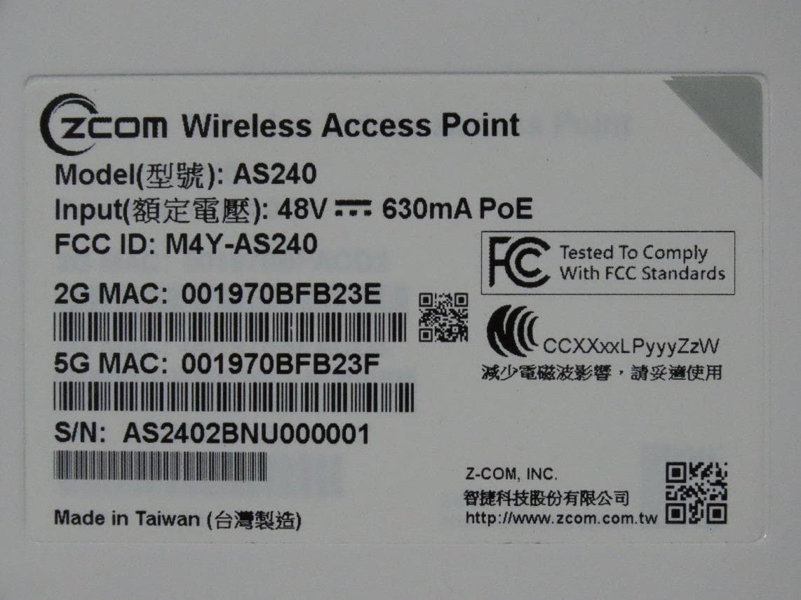
M4Y-AS240
Dec 13, 2022802.11ax Access Point
Equipment Class
DTS - Digital Transmission System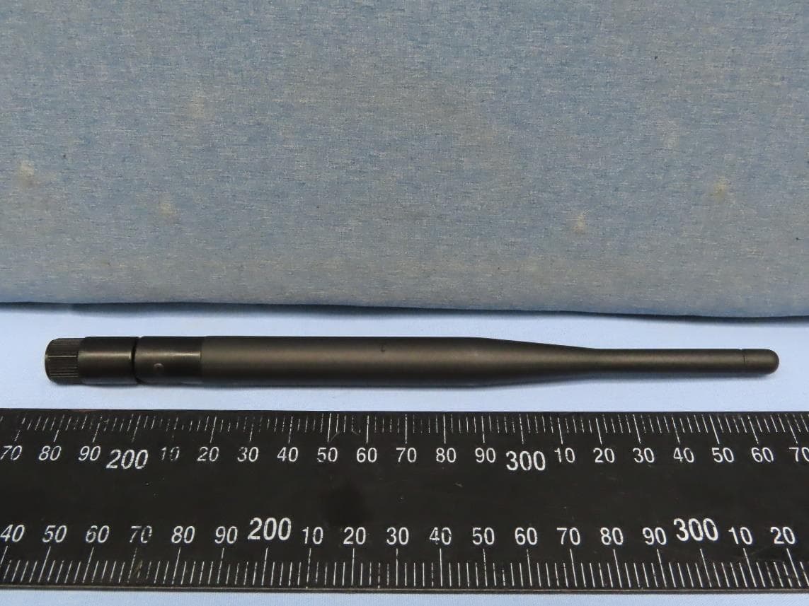
M4Y-AC720M
Aug 14, 2022802.11ac Wireless LAN USB Module
Equipment Class
NII - Unlicensed National Information Infrastructure TX
M4Y-SP230
Feb 21, 2021802.11 ac Wave 2 Access Point
Equipment Class
NII - Unlicensed National Information Infrastructure TX
M4Y-SP220C02
Jan 21, 2020802.11ac Access Point
Equipment Class
NII - Unlicensed National Information Infrastructure TX
M4Y-SP220C03
Jan 20, 20205GHz 11ac Wireless Bridge
Equipment Class
NII - Unlicensed National Information Infrastructure TX