M698836VGA Card
Sparkle Computer Co Ltd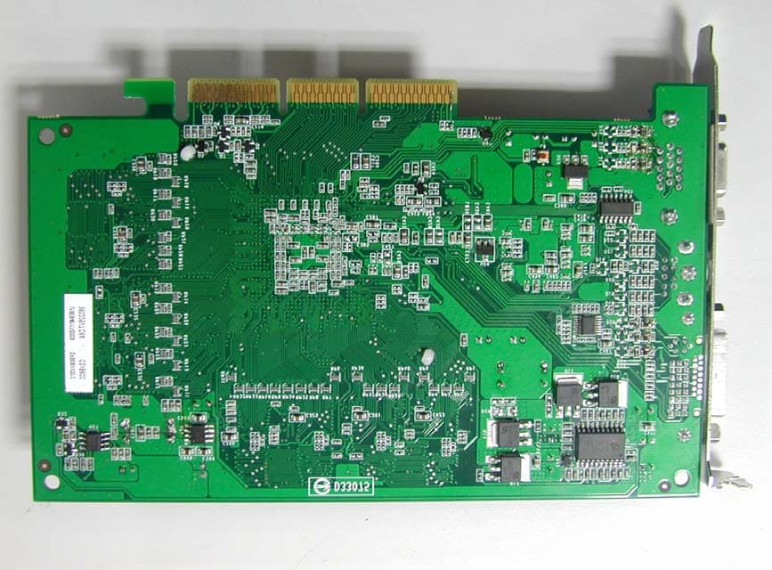
Click to zoom
Application Details
- Equipment Class
- JBP - Part 15 Class B Computing Device Peripheral
- Date of Grant
- Apr 14, 2004
- Application Purpose
- Original Equipment
- Date of Application
- Apr 14, 2004
- Equipment Note
- VGA Card
- Company
- Sparkle Computer Co Ltd
- Country
- Taiwan
Documents & Files
Document Text
Text extracted from the exhibit documents filed with the FCC. Open a document above to read the original.
Users Manual
SP8836 SPARKLE COMPUTER CO., LTD. 3D GRAPHIC ACCELERATOR MANUAL 1 5.5.1 GeForce4 FX 5700 (NVIDIA).................................................................11 5.5.2 nView Display Mode .............................................................................. 12 5.5.2.1 Standard mode ............................................................................ 13 5.5.2.2 Color correction... ........................................................................ 14 5.5.2.3 Device Adjustments ..................................................................... 15 5.5.2.4 Display Timing ............................................................................. 16 5.5.2.5 nView enable mode..................................................................... 17 5.5.3 Performance & Quality Setting............................................................... 19 5.5.3.1 Direct3D Setting........................................................................... 20 5.5.3.2 OpenGL Setting ........................................................................... 21 5.5.4 Overlay Controls .................................................................................... 22 5.5.5 Trouble shooting .................................................................................... 23 5.5.6 NVRotate ............................................................................................... 24 5.5.7 Temperature Settings (optional)............................................................. 25 5.5.8 Refresh Rate Overrides ......................................................................... 26 5.5.9 Change Resolutions............................................................................... 27 5.5.10 Desktop Management.......................................................................... 28 5.5.11 Screen Menus...................................................................................... 29 6. Manually installing Windows 98 and Windows ME drivers ........................................ 30 6.1 Removing old Drivers: (only if you have old NVIDIA drivers)............................ 30 6.2 Installation and Setup ...................................................................................... 30 6.3 How to Change Color Depth and Resolution.................................................... 31 6.4 How to Change Refresh Rate.......................................................................... 31 7. Manually install Windows 2000 drivers ..................................................................... 32 FCC Statement............................................................................................................. 33 Trademark Acknowledgments ...................................................................................... 33 2 NVIDIA CineFX 2.0 engine -Support for DX 9 pixel shader 2.0+ -Support for DX 9 vertex shader 2.0+ -Very long pixel programs up to 1024 instructions -Very long vertex programs with up to 256 static instructions and up to 65536 instructions executed before termination -Looping and subroutines with up to 256 loops per vertex program -Subroutines in shader programs -Dynamic flow control -Conditional write masking -Conditional execution -Procedural shading -Full instruction set for vertex and pixel programs -Z-correct bump-mapping -Hardware-accelerated shadow effects with shadow buffers -Two-sided stencil -Programmable matrix palette skinning -Keyframe animation -Custom lens effects: fish eye, wide angle, fresnel effects, water refraction High-performance, high-precision 3D rendering engine -4-pixels per clock rendering engine -128-bit, studio-quality floating point precision through the entire graphics pipeline -Native support for 128-bit floating point, 64-bit floating point and 32-bit integer rendering modes -Up to 16 textures per pass -Support for sRGB texture format for gamma textures -DirectX and S3TC texture compression High-performance 2D rendering engine -Optimized for 32-, 24-, 16-, 15- and 8-bpp modes -True-color, 64x64 hardware cursor with alpha -Multi-buffering (double, triple or quad) for smooth animation and video playback 3 need for panning with built-in Macrovision copy protection -DVD and HDTV-ready MPEG-2 decoding up to 1920x1080i resolutions -Dual, integrated 400MHz RAMDACs for display resolutions up to and including 2048x1536@85Hz -DVI Support for compatibility with next-generation flat panel displays with resolutions up to and including 1600x1200 -NVIDIA NVRotate™ application for advanced viewing flexibility -NVIDIA NVKeystone™ application for advanced display correction NVidia Digital Vibrance Control TM (DVC) 3.0 -DVC image sharpening controls -DVC color controls Rocket science for a system-level solution -0.13u process technology for higher levels of integration and higher operating clock speeds - Copper vias and wiring - Advanced thermal monitoring and thermal management - AGP 8X including Fast Writes and sideband addressing Broad operating system support -Windows® XP -Windows 2000 -Windows Me -Windows 9X API support -Comprehensive Microsoft DirectX 9.0 (and lower) support -OpenGL 1.5 (and lower) support Compatibility -NVIDIA Unified Driver Architecture (UDA) -Fully compliant professional OpenGL 1.5 API with NVIDIA extensions, on all Windows operating systems -WHQL-certified for Windows XP, Windows Me, Windows 2000 4 gp()pg pull straight out of the motherboard slot. If the card is stuck, rock from side to side to dislodge it. Remember to keep the screw. 4. Locate the empty slot in the motherboard and then install the card in the AGP bus slots 5. Replug the cable into the computer and replace the cover. 2.3 Installing notice (5700 Ultra only) 1. In order to make your system more stable, we recommend the minimum requirement for the power supply is 300 Watts. 2. To ensure optimal performance, verify that the Molex hard drive power connector is properly connected to the white port on the edge of t…
Text truncated - open the document above for the full version.
Block Diagram
SPARKLE SP8836 Block diagram: AGP BUS Memory BIOS VIVO/ TVout Nvidia GeForce FX 5700 X’TAL 27.000Mhz CRT DVI-I X’TAL 24.576Mhz
External Photos
NEUTRON EMC LAB. Project No.:04E0123 2/3 04E0123 04E0123 NEUTRON EMC LAB. Project No.:04E0123 3/3 04E0123
ID Label/Location Info
FCC ID: M698836
ID Label/Location Info
-- FCC ID label -- The remained portion of label statement required by FCC is attached in the user’s manual. -- Location of Label on EUT -- 4cm 0.5cm FCC ID: M698836 FCC ID: M698836
Internal Photos
NEUTRON EMC LAB. Project No.:04E0123 2/3 04E0123 04E0123 NEUTRON EMC LAB. Project No.:04E0123 3/3 04E0123
Operational Description
Operational Description The EUT is a VGA Card. Based on the application, features, or specification exhibited in User's Manual, the EUT is considered as an ITE/Computing Device. More details of EUT technical specification, please refer to the User's Manual
Schematics
55 44 33 22 11 D D C C B B A A NV_PGOOD NV_PGOOD 5V 12V 12V 12V FBVDDQ FBVDD FBVDDQ FBVTT (1.30V) (SOP-8-P & SOP-8 Option) Connected "Thermal Pad" ofAPL5331-KA to GND plane for better heat dissipation 6.3V X5R 0805 10% 10 V X7R 0805 10% 6.3V X5R 0805 10% 6.3V X5R 0805 10% A LE [email protected] 20% FBVTT Power Supply (SO-8) (SO-8) A LE 6.3V0.025R 2.09A@105C 20% A LE 6.3V0.025R 2.09A@105C 20% 20% A LE 0.44R0.23A@105C16 V 080516 V 10% X7R 3.02A@105C16 V +/-20% 0.030ROSCON 060316 V 10% X5R 080525 V 10% X7R FBVDDQ Power Supply NO STUFF forno powersequence FBVDDQ=0.8*(1+R6/R9)2.6V=0.8V*(1+2.26K/1K) 1.3V=2.6V*(1K(1K+/1K))FBVTT=FBVDDQ*(R3/(R3+R4)) Note : This circuit is for SOP-8 and SOP-8-P dual layout.If sop-8 can't priove enough t hermal dissipation, you can use sop-8-p package. R2961KRF0603 C6094.7uF0805 Q3A APM7313IC_SO8 2 71 8 D31 40V/2.1A DIODE_SMD_SMA 21 Q3B APM7313IC_SO8 4 53 6 R2925.1RJ0603 C6100.1uF0603 + C601150uFECD6 C6021uF0603 D301N4148SOT23 13 2 C6030.1uF0603 + C608470uFECD8 L311uHIND_CDR73 L324.7uHIND_MULTIPADS 1 23 4 C6170.01uF0603 R2890RJ0603 R2932.26KRF0603 D321N4148SOT23 13 2 R2945.1RJ0603 U27 APW7037A-KCIC_SO8 FB 1 VCC 2 LDRV 3 GND 4 HDRV 5 VC 6 COMP 7 SS 8 C5994.7uF0805 C6132200pF0603 C6051uF0603 + C611470uFCAPS_TH 1 2 3 C6154.7uF0805 + C612470uFCAPS_TH 1 2 3 R29524KRJ0603 ThermalPad Thermal Pad is GND U26APL5331 -KAC SOP_8_P VIN 1 GND 2 VREF 3 VOUT 4 NC3 5 VCNTL 6 NC2 7 NC1 8 9 9 R2901KRF0603 R2911KRF0603 C6041uF0603 R2885.1RJ0603 + C600100uFECD6 C6160.1uF0603 C6140.1uF0603 C6071uF0603 C6064.7uF0805 B1 121314 2 SKU 3456789 1011 NVPN 15 VARIANT ASSEMBLY 6001 01910001000 6001 01910000100 <UNDEF INED> <UNDEF INED> <UNDEF INED> 6001 01910000000 <UNDEF INED> <UNDEF INED> <UNDEF INED> <UNDEF INED> <UNDEF INED> <UNDEF INED> <UNDEF INED> <UNDEF INED> <UNDEF INED> <UNDEF INED> <UNDEF INED> <UNDEF INED> <UNDEF INED> <UNDEF INED> <UNDEF INED> <UNDEF INED> <UNDEFINED><UNDEFINED><UNDEFINED><UNDEFINED><UNDEFINED><UNDEFINED><UNDEFINED> BASE <UNDEFINED><UNDEFINED><UNDEFINED> 602- 10191-base-sch 602-10191-000 0-000 602-10191-000 1-000 <UNDEF INED> <UNDEF INED> <UNDEF INED> 602-10191-000 0-100 <UNDEF INED> <UNDEF INED> <UNDEFINED><UNDEFINED>NV36-U Gen 400/300 1 28MB 16Mx16 VGA+VIVO+DVINV36-U Gen 400/300 1 28MB 16Mx16 VGA+VIVO+DVINV36-U Gen 400/300 1 28MB 16Mx16 VGA+VO+DVI BASE LEVEL GENERIC SCHEMATIC ONLY, COMMON & NO _STUFF ASSEMBLY NOTES AND BOM NOT FINAL ASSEMBLY PAGE DETAIL IMPLIED WARRANTIES INCLUDING, WITHOUT LIMITATION, THE WARRANTI ES OF DESIGN, OF NONINFRINGEM ENT, MERCHANTABILITY OR FITN ESS FOR A PARTICULAR PURPOSE, OR ARISING FROM A COURSE OF DEALING, TRADE USAGE, TRADE PRACTICE, OR INDUSTRY STANDARDS. 1 E G C H G F E D C B A 12345 AB D F H 5432 ALL NVIDIA DESIGN SPECIFICATIONS, REFERENCE SPECIFICATIONS, REFERENCE BOARDS, FILES, DRA WINGS, DIAGNOSTICS, LISTS AND OTHER DOC UMENTS OR INFORMATION (TOGETHER AND SEPARATELY, 'MATERIALS') ARE BEING PROVIDED 'AS IS'. THE MATERIALS MAYCONTAIN KNOWN AND UNKNOWN VIOLATIONS OR DEVIATIONS OF INDUSTRY STANDARDS AND SPECIFICATIONS. NVIDIA M AKES NO WARRANTIES, EXPRESSED, IMPLIED, STATUTORY OR OTHERWISE WITH RESPECT TO THE MATERIALS OR OTHERWISE, AND EXPRESSLY DISCLAIMS ALL BASE LEVEL GENERIC SCHEMATIC ONLY, COMMON & NO _STUFF ASSEMBLY NOTES AND BOM NOT FINAL <edit here to insert page detail> 9/18/08: CLoned fromP191_A009/04/03: Page 21 - Added Silent Running 9/04/08: X-Released SPARKLE SP8836 REVl:C1.1 9/03/03: Page 21 - Added Schmoo two 10K (NO_STUFF) resistors for NVVDD Schmoo circuit. 8/27/03: Page 15 - C hanged R562 to a 0603 to facilitate routing 8/26/03: to a dual switcher (ISL6225) that generates FBVDD(Q) and FBVTT. 24. Strap Configurations19. BIOS serial ROM, Temperature Sensor, PWM Fan Control.13. DACA RGB and EMI filters, DB15 primary slim VGA connector 8/26/03: Page 6 - Added Low pass filter to GPU_VTT8/29/03: Page 21 - Remo ved C765 and connected U510.12 to U510.17 (NV_SFTSTRT) 8/26/03: The Li near Sink/Source that generat ed FVBTT was also removed. 8/26/03: Page(S) 22 - FBVDD(Q) power supply was changed fr om individual (HIP6012) switchers. 8/22/03: Page(S) 4,5,7,8) - Changed Memory termination to F BVTT parrallel and added de-coupling caps. 8/22/03: P191 wa s cloned from P193 23. FBVDDSwitcher20. Linear R egulators for A3V3, TMDSAB_PLLVDD, TMDSAB_IOVDD3. FBA partition, FBVDDQ decoupling, FBDLLVDDdecoupling10. DACA, DACB, DAC sync buffers, PLL, XTAL11. DACA RGB and EMI filters, DB15 primary slim VGA connector 12. Internal TMDS Link A+B, Internal TMDS DVI-I connector14. Internal TMDS Link C, Internal TMDS DVI-I connector8. FBC1 qty 2 8Mx16 DDR1 memories,decoupling.5. FBA1 qty 2 8Mx16 DDR1 memories,decoupling.4. FBA0 qty 2 8Mx16 DDR1 memories,decoupling.1. This page: Page summary, revision history and variant info table 9. Ground, Thermal grounds and NCs. 17. Mini Din Video In/Out Connector PAGE SUMMARY: 2.AGP/PCI7. FBC0 qty 2 8Mx16 DDR1 memories,decoupling.6. FBC partition, FBVTT, FBCAL22. FBVDDQSwitcher18. 4-pin Video-In, 10-pin Video-In Connector16. 7114 video capture 15. NV36 VIP, NV36DVOA21. NVVDDSwitcher. 8/26/03: Page 21 - Added 10K pullup to NV_PGOOD 9/18/03: Pages 2, 21 - A dded two resistors for Droop Compensation 9/18/03: Page 12 - Removed Link-B from design 9/18/03: Page 22 - Added test point for FBVTT 2003/12/26 page1 AGPADSTBF0 AGPADSTBF0 25MIL AGPADSTBF1 AGPADSTBF1 25MIL AGPADSTBS0 AGPADSTBS0 25MIL AGPADSTBS1 AGPADSTBS1 25MIL AGPCALPD_VDDQ AGPCALPD_VDDQ 20MIL AGPCALPU_GND AGPCALPU_GND 20MIL AGPDBI_HI AGPDBI_HI 20MIL AGPDBI_LO AGPDBI_LO 20MIL AGPMBDET AGPMBDET 10MIL 5MIL_TRACE AGPRBF AGPRBF 10MIL AGPSBA0 AGPSBA0 AGPSBA1 AGPSBA1 AGPSBA2 AGPSBA2 AGPSBA3 AGPSBA3 AGPSBA4 AGPSBA4 AGPSBA5 AGPSBA5 AGPSBA6 AGPSBA6 AGPSBA[7..0] AGPSBA[7..0] 20MIL AGPSBA7 AGPSBA7 AGPSBSTBF AGPSBSTBF 25MIL AGPSBSTBS AGPSBSTBS 25MIL AGPST0 AGPST0 20MIL AGPST1 AGPST1 20MIL AGPST2 AGPST2 20MIL AGPSTOP 10MIL 12MIL_TRACE AGPSTOP* AGPVREFCG AGPVREFCG 10MIL 12MIL_TRACE AGPVREFCG_GPU AGPVREFCG_GPU 10MIL 12MIL_TRACE AGPVREFGC AGPVREFGC 12MIL 12MIL_TR…
Text truncated - open the document above for the full version.
Test Report
NEUTRON EMC LAB. Report No.:NEI- FCC-E-04038 2/34 Declaration Neutron represents to the client that testing is done in accordance with standard procedures as applicable and that test instruments used has been calibrated with the standards traceable to National Measurement Laboratory (NML) of R.O.C., or National Institute of Standards and Technology (NIST) of U.S.A. Neutron's reports apply only to the specific samples tested under conditions. It is manufacture’s responsibility to ensure that additional production units of this model are manufactured with the identical electrical and mechanical components. Neutron shall have no liability for any declarations , inferences or generalizations drawn by the client or others from Neutron issued reports. Neutron’s reports must not be used by the client to claim product endorsement by the authorities or any agency of the Government. This report is the confidential property of the client. As a mutual protection to the clients, the public and Neutron-self, extracts from the test report shall not be reproduced except in full with Neutron’s authorized written approval. Neutron’s laboratory quality assurance procedures are in compliance with the ISO Guide 17025 requirements, and accredited by the conformity assessment authorities listed in this test report. Limitation For the use of the authority's logo is limited unless the Test Standard(s)/Scope(s)/Item(s) mentioned in this test report is (are) included in the conformity assessment authorities acceptance respective. Assessment Authorities Test Standard/Scope/Item Acceptance FCC Part 15 Subpart B IEC/CISPR22 AS/NZS CISPR 22 CNS 13438 FCC Part 15 Subpart B CISPR 22/EN 55022 AS/NZS CISPR 22 VCCI -Technical Requirement CNS 13438 SS IEC/CISPR 22 IEC/EN 61000-3-2 IEC/EN 61000-4-5 IEC/EN 61000-3-3 IEC/EN 61000-4-6 IEC/EN 61000-4-2 IEC/EN 61000-4-8 IEC/EN 61000-4-3 IEC/EN 61000-4-11 IEC/EN 61000-4-4 CISPR 22/EN 55022 IEC/EN 61000-3-2 IEC/EN 61000-4-5 IEC/EN 61000-3-3 IEC/EN 61000-4-6 IEC/EN 61000-4-2 IEC/EN 61000-4-8 IEC/EN 61000-4-3 IEC/EN 61000-4-11 IEC/EN 61000-4-4 VCCI -Technical Requirement NEUTRON EMC LAB. Report No.:NEI- FCC-E-04038 3/34 Table of Contents Page 1 General Information 5 1.1 Applicant 5 1.2 Manufacturer 5 1.3 Equipment Under Tested 5 1.4 OEM Brand/Model 5 1.5 Model Difference (Series, Versions, if any) 5 1.6 Product Description 6 1.7 Connecting I/O Port(s) 6 1.8 Power Supplied 6 1.9 Products Covered 6 1.10 Description of Test Mode(s) 6 1.11 EUT Modifications 6 1.12 Summary of Test Results 7 2 RFI Emissions Measurement 8 2.1 Test Facility 8 2.2 Standard Compliance 8 2.3 Test Methodology 8 2.4 Deviations from Standard Test Method 8 2.5 Sample(s) Tested 8 2.6 Measurement Instrument 8 2.7 Measurement Uncertainty 9 2.8 Tested System Set-Up/Configuration Details 9 Table -1 Equipments Used in Tested System 10 Diagram -1 Block diagram showing the configuration of system tested 11 Table - 2 Equipments Used in Tested System 12 Table - 3 Information of Interface Cable 12 2.9 EUT Operating Conditions 13 3 Justification 14 3.1 Limitations 14 3.1.1 Power Line Conducted Emission 14 3.1.2 Radiated Emission Limits 14 3.2 Measurement Justification 15 3.2.1 Conducted Emission 15 3.2.2 Radiated Emission 15 3.3 Measurement Data 15 Table 4 Conducted Emission Data 16 Table 5 Radiated Emission Data 21 NEUTRON EMC LAB. Report No.:NEI- FCC-E-04038 4/34 Table of Contents Page Attachment 26 A. EUT Modification Description 27 B. EUT Test Photos 28 NEUTRON EMC LAB. Report No.:NEI- FCC-E-04038 5/34 1. General Information 1.1 Applicant Name SPARKLE COMPUTER CO., LTD. Address 13F, NO. 2, SEC. 1, FU HSING S. RD., TAIPEI, 104 TAIWAN, R.O.C. 1.2 Manufacturer Name N/A Address N/A 1.3 Equipment Under Tested Name: VGA Card Trade Name: SPARKLE Model No.: SP8836; SP8836F7/256MB; SP8836F7/128MB 1.4 OEM Brand/Model (if applicable) OEM Brand(s)/Model(s) except the basic model in sub-clause 1.3 is(are) the follows: OEM Brand: N/A Model No.: N/A 1.5 Model Difference (Series, Versions, if any) Except the basic model no. (model designation of the sample tested in this test report), additional model no. covered is(are) : There are three models based on similar electrical circuit except the difference of list below: Model No. DDR SP8836 16X16DDR SP8836F7/256MB 16X16DDR SP8836F7/128MB 8X16DDR All the above models were tested, and the model: SP8836 was found to be the worst case during the pr-scanning test. This mode of the worst case was used for final testing and collecting test data included in this report. NEUTRON EMC LAB. Report No.:NEI- FCC-E-04038 6/34 1.6 Product Descriptions(Application/Features/Specification) The EUT is a VGA Card. Based on the application, features, or specification exhibited in User's Manual, the EUT is considered as an ITE/Computing Device. More details of EUT technical specification, please refer to the User's Manual 1.7 Connecting I/O Port(s) Please refer to the User's Manual 1.8 Power Supplied Power Source : Supplied from AGP bus. Power Cord : N/A Power Rating : N/A 1.9 Products Covered (if applicable) The sample tested including the following sub-system/module/accessory : Sub-system/ Module/ Accessory Model/Type No. Int. Inst./ Ext. Cont. N/A N/A N/A 1.10 Description of Test Mode(s) To investigate the maximum EMI emission characteristics generates from EUT, the test system was pre-scanning tested base on the consideration of following EUT operation mode or test configuration mode which possible have effect on EMI emission level. Each of these EUT operation mode(s) or test configuration mode(s) mentioned above was evaluated respectively. Mode 1 1600*1200/106KHz/85Hz VGA and DVI Port (CRT & Projector) - “H” pattern Mode 2 1024*768/99KHz/120Hz VGA and DVI Port (CRT & Projector) - “H” pattern Mode 3 800*600/98KHz/150Hz VGA and DVI Port (CRT & Projector) - “H” pattern Mode 4 1024*768/48KHz/120Hz DVI and S-Video Port (Projector & TV) - “Color Bar” pattern Mode 5 1024*768/48KHz/120Hz VGA and AV Port (CRT & TV) - …
Text truncated - open the document above for the full version.
Test Setup Photos
NEUTRON EMC LAB. Report No.:NEI- FCC-E-04038 29/34 Conducted Measurement Photos Mode 1, 2, and 3 NEUTRON EMC LAB. Report No.:NEI- FCC-E-04038 30/34 Conducted Measurement Photos Mode 4 NEUTRON EMC LAB. Report No.:NEI- FCC-E-04038 31/34 Conducted Measurement Photos Mode 5 NEUTRON EMC LAB. Report No.:NEI- FCC-E-04038 32/34 Radiated Measurement Photos Mode 1, 2, and 3 NEUTRON EMC LAB. Report No.:NEI- FCC-E-04038 33/34 Radiated Measurement Photos Mode 4 NEUTRON EMC LAB. Report No.:NEI- FCC-E-04038 34/34 Radiated Measurement Photos Mode 5
Contact Information
Applicant
Jack Hsiao(Manager)
886 2 2741-1196Fax: 886 2 2711-7692
Test Firm
BTL Inc.Andy Chiu
Technical Specifications
| # | Rule Parts | Frequency Range | Power Output |
|---|---|---|---|
| 1 | 15B | - | - |
Other Applications from Sparkle Computer Co Ltd
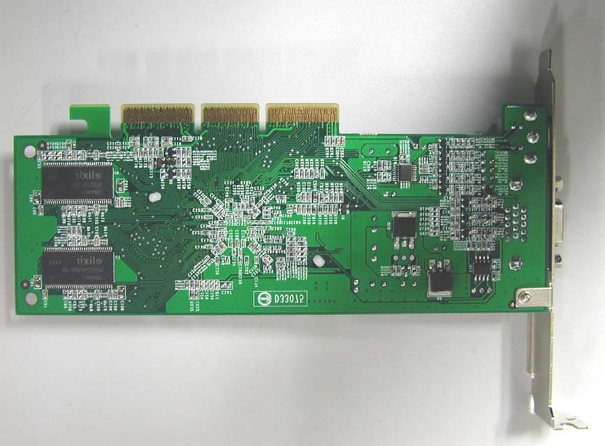
M697310
Mar 30, 2004VGA Card
Equipment Class
JBP - Part 15 Class B Computing Device Peripheral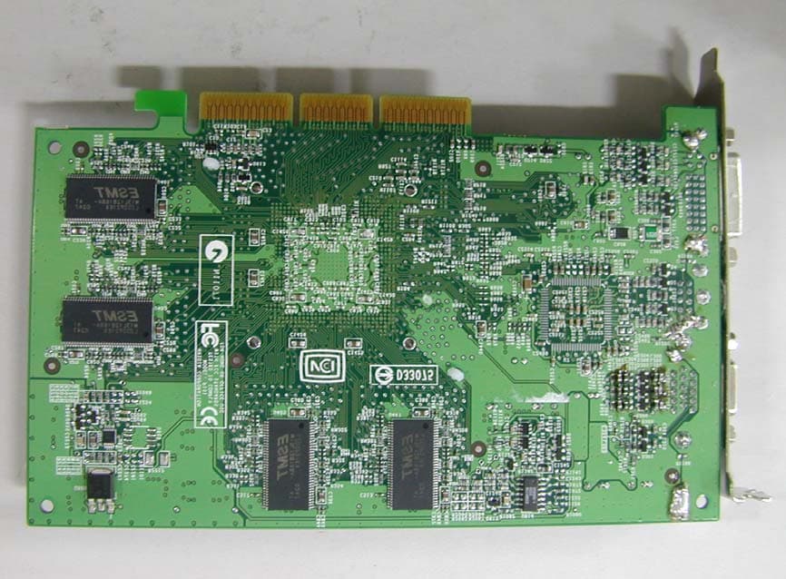
M697228T2
Feb 04, 2003VGA Card
Equipment Class
JBP - Part 15 Class B Computing Device Peripheral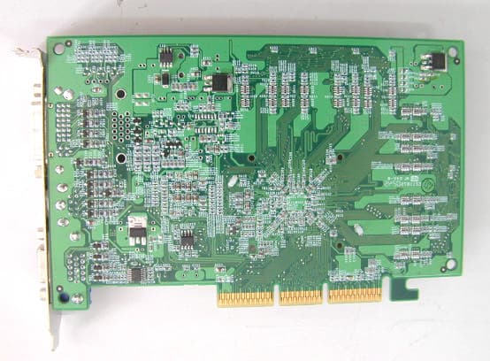
M697300M4
Feb 04, 2003VGA Card
Equipment Class
JBP - Part 15 Class B Computing Device Peripheral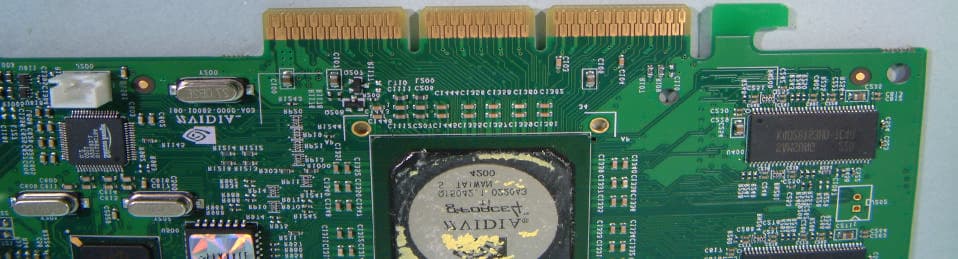
M697200T2
Dec 30, 2002VGA Card
Equipment Class
JBP - Part 15 Class B Computing Device Peripheral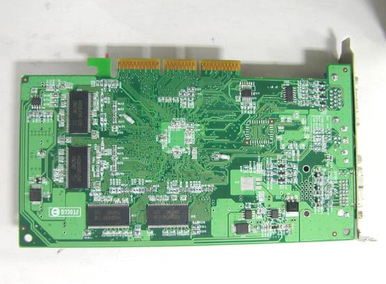
M697100A3
Nov 21, 2002VGA Card
Equipment Class
JBP - Part 15 Class B Computing Device Peripheral