MMA70201BDUHF Transceiver
Midland Radio Corporation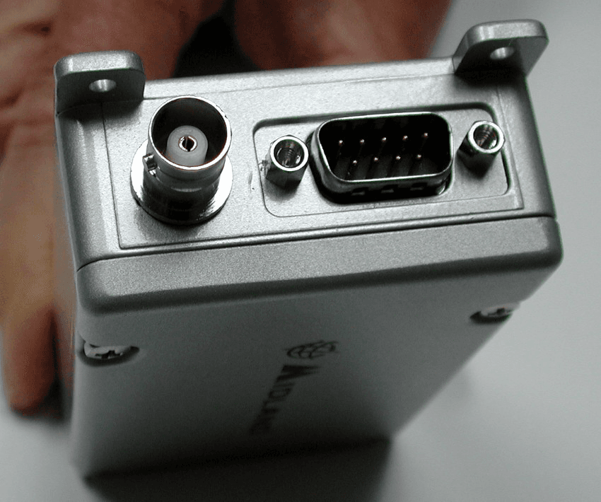
Click to zoom
Application Details
- Equipment Class
- TNB - Licensed Non-Broadcast Station Transmitter
- Date of Grant
- Oct 09, 2002
- Application Purpose
- Original Equipment
- Date of Application
- Oct 09, 2002
- Equipment Note
- UHF Transceiver
- Frequency Range
- 440.00000000 - 470.00000000
- Company
- Midland Radio Corporation
- Country
- United States
Documents & Files
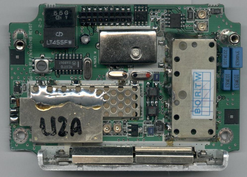
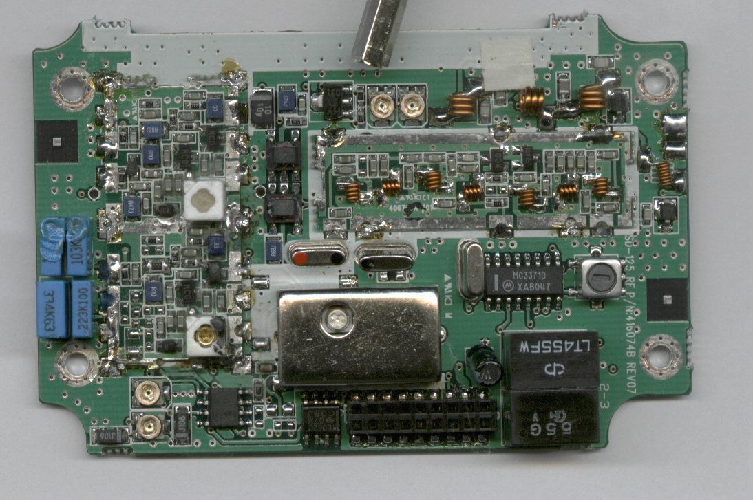
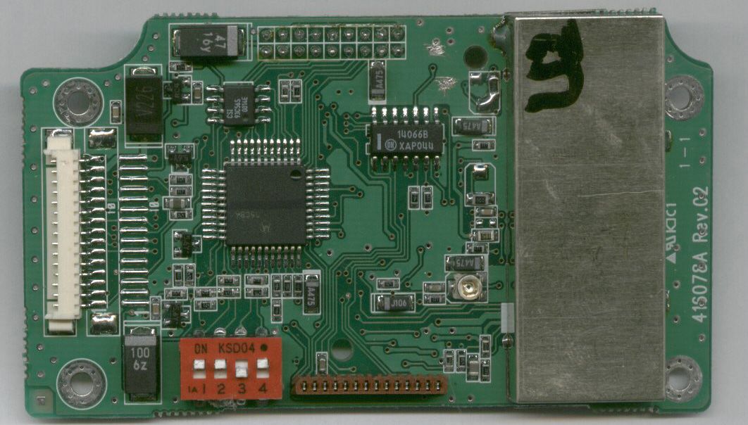
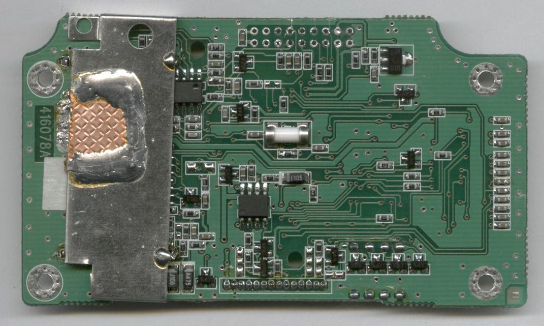
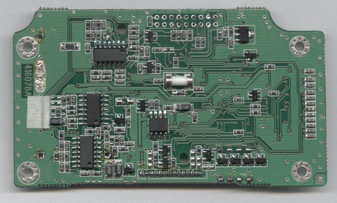
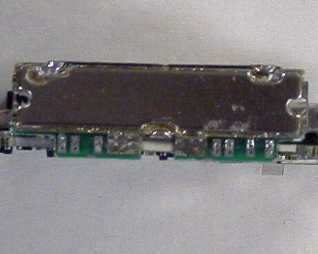
Document Text
Text extracted from the exhibit documents filed with the FCC. Open a document above to read the original.
Users Manual
1 SERVICE MANUAL RF DATA LINK RADIOS 70-101BD 70-201BD Important Information 2 All rights reserved. No part of this publication may be reproduced, transmitted, transcribed, stored in a retrieval system, or translated into any language without the written permission of Midland Radio Corporation No part of any copyrighted computer programs contained in the products referred to in this manual may be copied or reproduced without the express written consent of Midland Radio Corporation Midland Radio Corporation reserves the right to change the products described in this manual without prior notice. © Midland Radio Corporation This manual is designed to facilitate the set-up and service of the Midland 70- 101BD and 70-201BD RF Data Link Radio series. As necessary, service manual supplements will be published and distributed on the following forms: Manual Addition (MA)...............For supplemental information useful in product service or improvement. Printed on BLUE paper. Change Notice (CN)...............For details about changes made during production by model and serial number. Printed on YELLOW paper. Manual Correction (MC).......For correcting literature errors not related to production changes. Printed on GREEN paper. Technical Bulletin (TB)..........For solutions to field problems and tips for performance improvement. Printed on PINK paper. 3 Comments or suggestions concerning areas of manual improvement are welcome. 4 TABLE OF CONTENTS Manual Supplement Information.....................................................................ii Table of Contents...........................................................................................iii Acronyms and Abbreviations.........................................................................iv GENERAL INFORMATION Specifications...................................................................................................1-3 PREPARATION Test Equipment................................................................................................4 Alignment Points...............................................................................................5 Complete Realignment......................................................................................6-7 CIRCUIT DESCRIPTION Description.......................................................................................................8-11 SERVICE Maintenance and Repair ..................................................................................12-13 Trouble shooting guide......................................................................................14 Voltage Charts..................................................................................................15-18 Component Pinout............................................................................................19-22 DIAGRAMS Block Diagram..................................................................................................23 Wiring Diagram.................................................................................................24 TCXO Schematic..............................................................................................24 VCO (148-174MHz) Schematic..........................................................................25 VCO (440-470MHz) Schematic..........................................................................25 Front End (148-174MHz) Schematic..................................................................26 Front End (440-470MHz) Schematic..................................................................26 PA (148-174MHz) Schematic............................................................................26 PA (440-470MHz) Schematic............................................................................26 RF Board (148-174MHz) Schematic...................................................................27 RF Board (440-470MHz) Schematic...................................................................28 Digital Board Schematic....................................................................................29 RF Board View (148-174MHz) Layout................................................................30 RF Board View (440-470MHz) Layout................................................................31 Digital Board View Layout.................................................................................32 70-101/201BD Exploded View...........................................................................33 PARTS 70-101BD RF Board Parts List...........................................................................35-38 70-201BD RF Board Parts List...........................................................................39-42 Digital Board Parts List......................................................................................43-45 Replacement Parts Ordering.............................................................................46 5 ACRONYMS AND ABBREVIATIONS Below is a list of common electrical abbreviations used in documentation. CTCSS----------------------- Continuous Tone-Controlled Squelch System DCS(or CDCSS) ---------- Continuous Digital-Controlled Squelch System EEPROM ------------------ Electrically Erasable Programmable Read Only Memory MIL SPEC ------------------ Military Specification RX --------------------------- Receive TX --------------------------- Transmit SINAD ---------------------- The ratio in decibels of signal + noise + distortion to noise + distortion VCO ------------------------ Voltage Controlled Oscillator TCXO ---------------------- Temperature Controlled Crystal Oscillator PLL ------------------------- Phase Locked Loop Installation and Setup Information for 70-101BD and 70-201BD Data Link Radios. Transmit/Receive channels are chosen from the frequencies programmed by switches inside the cover. Refer to the channel data list and set DIP switches for the desired frequency. 6 All connec…
Text truncated - open the document above for the full version.
Operational Description
Description 70-101BD & 70-201BD © Midland Radio Corporation 8 THEORY OF OPERATION INTRODUCTION The Midland 70-101/201BD series of RF Link Modules utilizes the latest technology in its design and manufacturing. Both the UHF and VHF models are PLL (Phase Lock Loop Synthesizer)/microprocessor controlled, and offers one to five watts of power with 16 channel capability. Multiple functions including 1200 to 19,200 baud rates, AC and/or DC audio coupling, GMSK and FSK modulation are standard in these fully programmable wide bandwidth RF Link Module units. The radio is programmed using an IBM Personal Computer, DOS based software, an interface module and a programming cable. This allows the radio to be tailored to meet the requirements of the individual user and of the System(s) it is operating within. The VHF and UHF radios are composed of two PCB’s (a RF PCB and a digital PCB). These boards are connected with an 18 pin female and male connector. The digital board is interfaced with external data equipment through the 9 pin d-sub male connector, which controls the radio and data receiving and sending. DIGITAL CIRCUITS The Digital circuit contains the CPU, the channel select switch, and associated digital circuits. TX-SIGNAL CIRCUIT The TX data signal comes from Pin 2 of Con401, and goes through U404D. The TX-signal is filtered by U405A & B which is a 4’th order low pass filter, the output of U405A is then fed to the RF board for TX modulation. The TX microphone signal comes from pin 7 of Con401 through U405D, the pre-emphasis network, and U405C. The output level is set by RV402 before mixing with other AF signal inputs at U406C. RX-SIGNAL CIRCUIT The RX-data signal comes from the RF board, which is connected with pin 10 of Con403. The RX- signal is switched by U404A and adjusted by RV403 and amplified by U407. The amplified signal goes to pin10 of Con401. RSSI DETECTOR From the RF board, the RSSI (Received Signal Strength Indicator) signal flows to U403A & B through R461. The pulse is injected from pin5 of U403B every 1mS and C451 is discharged. It is then charged by R464. The RSSI signal is simultaneously input to pin 7 of U403A and those signals are compared. The compared signal is output from U403A. Pin 1 of U403A and the CPU detects the pulse width. The pulse width is varied by RSSI DC voltage, therefore, the carrier detection is controlled by the CPU. EEPROM RX/TX channel and RSSI detection level as well as other data from the programmer are stored in the EEPROM. The data stored is retained without power supplied. This is a non-volatile memory. The EEPROM may have information re-programmed or erased. U402 is an EEPROM with 2048 (8 x 256) capacity and data is written and read serially. Description 70-101BD & 70-201BD © Midland Radio Corporation 9 CHANNEL SELECTOR One of 16 channels may be selected using the Dip Switch (SW401). SW401 encodes the channel number, selected into 4-bit binary code. The binary code plus one equals the channel number. The binary code is decoded by the CPU enabling the appropriate RX or TX frequency and associated data to be selected from the EEPROM. DC TO DC CONVERTER The main DC power is injected to the DC to DC converter. The DC to DC converter regulates the various input power supply voltage and outputs a constant voltage of 7.5 Volts. It is a source for all of the RF and digital circuits. The DC to DC converter is formed by U801, Q801, Q802, L801 and R804. U801 is a switch mode DC to DC converter IC. Input DC various appears as a voltage and controls the switching pulse. As the switching pulses, Q801 and Q802 switches the input Dc of various supply voltages and generates the constant DC of supply voltage. RF CIRCUITS TRANSMITTER The transmitter is comprised of: 1. Buffer 2. P.A. Module 3. Low Pass Filter 4. Antenna Switch 5. A.P.C. Circuits BUFFER VCO output level is –6dBm and amplified to +10dBm (UHF), +6dBm (VHF). The buffer consists of Q16 and Q17 for isolation and gain. P.A. MODULE The P.A. Module contains Q501, Q502, and Q503. Three stage amplifier Q501 amplifies the TX signal from +10dBm to 100 mW. Q502 is amplified to 0.5W. Q503 amplifies to 3W and then matched to 50 Ohms using the L.C. network, thereby reducing the harmonics by –30dB. LOW PASS FILTER L7, L8, L11, C72, C73, C74, AND C75 are the 7 th order Chebyshev low pass filter. Unwanted harmonics are reduced by –70dBc. ANTENNA SWITCH When transmitting, the diodes D5 and D6 are forward biased enabling the RF signal passage to the antenna. D6 is shorted to ground inhibiting the RF signal to front end. In receive the diodes D5 and D6 are reversed biased passing the signal from the antenna through L13 and C83 to the front end without signal loss. Description 70-101BD & 70-201BD © Midland Radio Corporation 10 AUTOMATIC CURRENT CONTROL (ACC) CIRCUITS The ACC circuit consists of R109, variable resistor RV1, IC3 (B) and transistors Q21 and Q22. The supply current is monitored by the difference voltage on R109 (0.1 Ohm). If the current varies by RF power output or other reasons, it produces some bias voltage by IC3A and Q19. The differential signal at the output of IC3 is passed to Q21 and Q22 that produces a constant power output to the antenna. RV1 is used to adjust the RF power level. RF CIRCUITS PLL SYNTHESIZER 12.8 MHz TCXO The TCXO contains the 3-stage thermistor network compensation and crystal oscillator and modulation ports. Compensation is –5ppm or less from –30C to +60C. PLL IC DUAL MODULES PRESCALER Input frequency of 12.8MHz to IC2 MC14519 pin 20 is divided to 6.25kHz or 5kHz by the reference counter, and then supplied to the comparator. RF signal input from VCO is divided to 1/64 at the prescaler in IC2, divided by A and N counter in IC2 to determine frequency steps, and then supplied to the comparator. PLL comparison frequency is 6.25/5kHz so that minimum programmable frequency step is 5/6.25kHz. The A and N counter is programmed to obtain the desired frequency by serial data in the CPU. In t…
Text truncated - open the document above for the full version.
Parts List/Tune Up Info
Preparation 70-101BD & 201BD © Midland Radio Corporation 6 PROGRAMMING The 70-101BD & 70-201BD series radio requires the 70-1410K Programming Kit, including programming software interface module, and programmer interface cable. ALIGNMENT PROCEDURE THE 70-x01BD UHF/VHF Receiver is by design, broad band covering UHF (440-470MHz) and VHF (148- 174MHz) and should require no special alignment, unless repairs are performed on the receiver portion. Should repairs be necessary, use the “Test Equipment Diagram” and the “Alignment Points Diagram”, in conjunction with the following procedures: An Extender Board (P/N: 70-075845) is required in order to separate the Digital and RF PCBs to allow access to the alignment points. Installation instructions are provided with the Extender Board Assembly. RECEIVER 1. Apply a standard test signal to the receiver antenna terminals. 2. Adjust T1 for maximum sensitivity and audio output with minimum audio distortion. 3. Adjust RV403 for the specific audio output level. RX VCO 1. Set the unit to the highest receive frequency, 470MHz (UHF)m 174MHz (VHF) and adjust the VCO L303 8 volts. 2. Set the unit to the lowest receive frequency, 440MHz (UHF), 148 (VHF) and check that the VCO voltage is above 2.0 volts. If voltage is below 2.0 volts, adjust L303 for 2.0 volts or more. Note: Use TP1 to measure the voltage. TRANSMITTER Connect the unit to a Service Monitor with the power meter setting to the 10W scale (or autorange). TCXO Set the channel selector to the mid-range frequency 460MHz, adjust TCX01 for a reading of 460MHz – 200Hz (155MHz VHF models. TX VCO 1. Set the unit to the highest transmit frequency, 470MHz (UHF), 174MHz (VHF) key the transmitter and adjust the VCO L203 to 8 volts. 2. Set the unit to the lowest transmit frequency 440MHz (UHF), 148MHz (VHF) key the transmitter and check that the Vco voltage is above 2.0 volts. If voltage is below 2.0 volts, adjust L203 for 2.0 volts or more. Note: Use TP1 to measure the voltage. TX Deviation and Balance Adjustment 1. Set the unit to a mid frequency and input the TX data with 400Hz standard audio level. 2. Increase the signal level to 20dB from standard level. 3. Monitor the demodulated signal from service monitor. Adjust RV3 to make the monitored signal to be a balanced square wave. Preparation 70-101BD & 201BD © Midland Radio Corporation 7 4. Reduce input signal to the standard level and adjust RV2 for the standard deviation. APC 1. Adjust RV1 for High Power (5W). 2. Adjust RV6 for Low Power (1W). 3. This completes the transmitter alignment procedures. 70-x01BD Squelch setting using 70-1410K Programming Kit The squelch level setting to open or close (mute or unmute) on the 70-101BD and 70-201Bd is performed by software control. The RSSI utilizes the A/D conversion that will be fed to the microprocessor, which in turn will use this input to determine the squelch level setting to control the mute and unmute of the receiver. Default setting of squelch level for all the 70-x01BD from our manufacture and workshop is approximately set at: 1. Squelch open (unmute) at –114dBm to –113dBm (0.45 – 0.5mV of the RX signal strength). 2. Squelch close (mute) at –117dBm to –116dBm (0.3 – 0.35mV of the RX signal strength). Changing the default squelch settings requires use of the programming adaptor box. This box is designed for use, not only as part of the programming kit, but also as a tool of squelch level setting. The minimum equipment required for squelch level setting is a RF signal generator. Radio communication test equipment is recommended. 1. Power up the programming adaptor box (use the DC supply of 9-15 Volts 200mA). 2. Hook up the 70-x01BD unit to the programming adaptor box, and its antenna connector to the RF input port of the RF signal generator. 3. With the adaptor box turned “off”, simultaneously press and hold both “ON/OFF” and “WRITE” buttons down. 4. Release the “ON/OFF” button first then the “WRITE” button next. LED indicator on the box will flash twice, after that it may stay on / off, this is of no concern. Depending on the signal strength of the RF generator, as well as the pre-set level of squelch, the 70-x01BD may be in standby mode (LED OFF) or in receiving mode (LED ON). 5. Adjust the RF signal generator for the desired signal strength to OPEN squelch (e.g. default setting is –113dBm, that is equivalent to 0.5mV). 6. Press and release “READ” button, LED indicator will flash 3 times then it will be ON. 7. Adjust the RF signal generator for the desired signal strength to CLOSE squelch (e.g. default setting is –116dBm, that is equivalent to 0.35mV). 8. Press and release “READ” button, LED indicator will flash 1 time then it will be OFF. 9. Press and release “WRITE” button, LED indicator will flash twice. 10. Squelch level is now set. Test for desired level by increasing or decreasing the RF signal to levels set for open and close squelch (mute LED will be OFF & unmute LED will be ON). Note: The difference of RF signal strength between the unmute and mute levels must be greater than or at least equal to 0.15mV (i.e. at least –123.5dBm) for the squelch setting to work properly. If they are too close to one another, RSSI through the A/D conversion con not differentiate between the mute and unmute level properly. As a result, it would cause the CD (Carrier Detect) to act intermittently.
Test Report
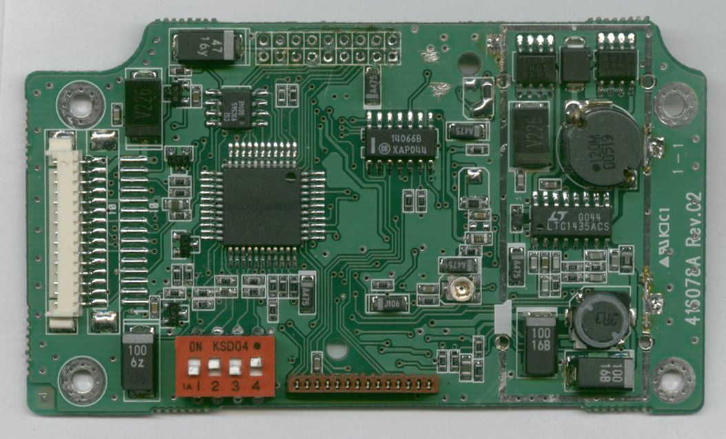
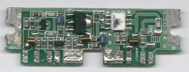
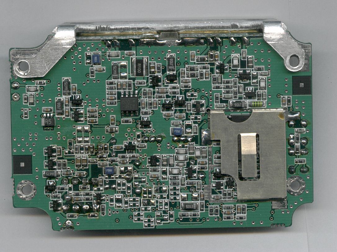
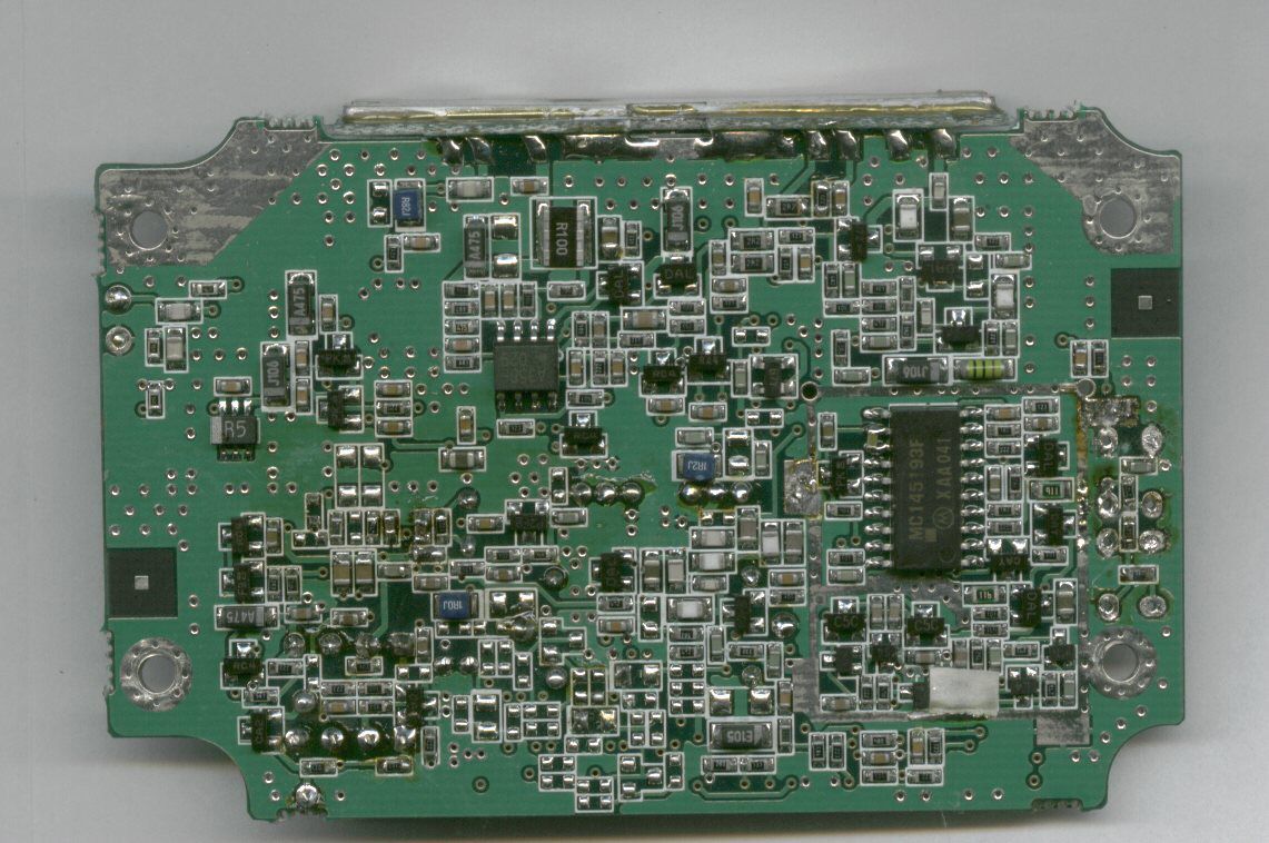
APPLICANT: MIDLAND RADIO CORPORATION FCC ID: MMA70201BD REPORT #: T:\M\MidlandRadio_MMA\924ut2\924UT2TestReport.doc TABLE OF CONTENTS TABLE OF CONTENTS LIST FOR PART 90 UHF DEVICE APPLICANT: MIDLAND RADIO CORPORATION FCC ID: MMA70201BD TEST REPORT: PAGE 1......COVER SHEET - GENERAL INFORMATION & TECHNICAL DESCR. PAGE 2......TECHNICAL DESCRIPTION CONTINUED PAGE 3......RF POWER OUTPUT, PAGE 4......MOD CHARACTERISTICS PAGE 5......AUDIO FREQUENCY RESPONSE PLOT PAGE 6-11...MODULATION LIMITING PLOTS PAGE 12.....AUDIO LOW PASS FILTER PLOT PAGE 13-14..OCCUPIED BANDWIDTH PAGE 15-19..OCCUPIED BANDWIDTH PLOTS PAGE 20.....SPURIOUS EMISSIONS AT ANTENNA TERMINALS PAGE 21.....METHOD OF MEASURING SPURIOUS EMISSIONS AT ANTENNA TERM. PAGE 22-23..FIELD STRENGTH OF SPURIOUS EMISSIONS PAGE 24.....METHOD OF MEASURING RADIATED SPURIOUS EMISSIONS PAGE 25.....FREQUENCY STABILITY PAGE 26-27..TRANSIENT FREQUENCY STABILITY PAGE 29-29..TRANSIENT FREQUENCY RESPONSE PLOTS – 12.5 kHz LOW POWER PAGE 30-31..TRANSIENT FREQUENCY RESPONSE PLOTS – 12.5 kHz HIGH POWER PAGE 32-33..TRANSIENT FREQUENCY RESPONSE PLOTS – 25 kHz LOW POWER PAGE 34-35..TRANSIENT FREQUENCY RESPONSE PLOTS – 25 kHz HIGH POWER PAGE 36-37..SPECTRAL EFFICIENCY PROC. & PLOTS – 9600 & 19200 baud PAGE 38-40..LIST OF TEST EQUIPMENT EXHIBITS CONTAINING: EXHIBIT 1.........FCC ID LABEL SAMPLE EXHIBIT 2.........LABEL LOCATION EXHIBIT 3.........SCHEMATICS EXHIBIT 4.........BLOCK DIAGRAM EXHIBIT 5.........THEORY OF OPERATION EXHIBIT 6.........EXTERNAL PHOTOGRAPHS EXHIBIT 7.........INTERNAL PHOTOGRAPHS – COMPONENT VIEW EXHIBIT 8.........INTERNAL PHOTOGRAPHS – COPPER VIEW EXHIBIT 9.........ALIGNMENT PROCEDURE EXHIBIT 10........USER MANUAL EXHIBIT 11........TEST SET-UP PHOTO APPLICANT: MIDLAND RADIO CORPORATION FCC ID: MMA70201BD REPORT #: T:\M\MidlandRadio_MMA\924ut2\924UT2TestReport.doc Page 1 of 40 GENERAL INFORMATION REQUIRED FOR TYPE ACCEPTANCE 2.1033 MIDLAND RADIO CORPORATION will sell the (c)(1)(2) FCC ID: MMA70201BD VHF transceiver in quantity, for use under FCC RULES PART 90, 22, 74 2.1033 (c) TECHNICAL DESCRIPTION 2.1033 (3) User Manual See Exhibit 13 2.1033 (4) Type of Emission: 20K0F3D For 25 kHz 90.209 11K25F3D For 12.5 kHz 11K0F3E For 12.5 kHz 18K0F3E For 25 kHz For 25 kHz Bn = 2M + 2DK M = 19,200 Bits per second D = 0.40 kHz (Peak Deviation) K = 1 Bn = 2(19200/2) + 2(400)(1) = 19.2k + 0.8k = 20.0k 90.209(b)(5) AUTHORIZED BANDWIDTH = 20.00 kHz. For 12.5 kHz Bn = 2M + 2DK M = 9,600 Bits per second D = 0.825 kHz (Peak Deviation) K = 1 Bn = 2(9600/2) + 2(0.825k)(1) = 9.6k + 1.65k = 11.25k 90.209(b)(5) AUTHORIZED BANDWIDTH = 11.25 kHz. For 12.5 kHz Bn = 2M + 2DK M = 3000 Hz D = 2.5 kHz (Peak Deviation) K = 1 Bn = 2(3000) + 2(2.5)(1) = 6k + 5k= 11k 90.209(b)(5) AUTHORIZED BANDWIDTH = 11.25 kHz. For 25 kHz Bn = 2M + 2DK M = 3000 Hz D = 6000 Hz (Peak Deviation) K = 1 Bn = 2(3000) + 2(6000) = 6k + 12k = 18k 90.209(b)(5) AUTHORIZED BANDWIDTH = 20.00 kHz. APPLICANT: MIDLAND RADIO CORPORATION FCC ID: MMA70201BD REPORT #: T:\M\MidlandRadio_MMA\924ut2\924UT2TestReport.doc Page 2 of 40 2.1033(c)(5) Frequency Range: 440-470 MHz 2.1033(c)(6) Power Range and Controls: There are NO user Power controls. 2.1033(c)(7) Maximum Output Power Rating: 5/1 Watts, into a 50 ohm resistive load. 2.1033(c)(8) DC Voltages and Current into Final Amplifier: Power Input – See next page. 2.1033(c)(9) Tune-up procedure. The tune-up procedure is given in EXHIBIT 12. 2.1033(c)(10) Complete Circuit Diagrams: The circuit diagram is included as EXHIBIT 3. The block diagram is included as EXHIBIT 4. Instruction book. The instruction manual is included as EXHIBIT 13. 2.1033(c)(11) A photograph or drawing of the equipment identification label is shown in Exhibit 1. 2.1033(c)(12) Photographs of the equipment of sufficient clarity to reveal equipment construction and layout and label location are shown in Exhibit 7-11. 2.1033(c)(13) For equipment employing digital modulation, a detailed description of the modulation technique. This UUT uses FSK to modulate the transmitter. 2.1033(c)(14) data required for 2.1046 to 2.1057 See Below 90.203(e) There are NO user controls and the frequency of this unit must be programmed using software not provided to the end user. APPLICANT: MIDLAND RADIO CORPORATION FCC ID: MMA70201BD REPORT #: T:\M\MidlandRadio_MMA\924ut2\924UT2TestReport.doc Page 3 of 40 2.1046(a) RF power output. RF power is measured by connecting a 50 ohm, re- sistive wattmeter to the RF output connector. With a nominal battery voltage of 12.0 VDC, and the transmitter properly adjusted the RF output measures: POWER OUTPUT INPUT POWER - HIGH: (12V)(1.380A) = 16.56 Watts INPUT POWER – LOW: (12V)(.640A) = 7.68 Watts OUTPUT POWER: HIGH - 5 Watts LOW - 1 Watts METHOD OF MEASURING RF POWER OUTPUT Transmitter 50 ohm under test Resistive Wattmeter Power Supply APPLICANT: MIDLAND RADIO CORPORATION FCC ID: MMA70201BD REPORT #: T:\M\MidlandRadio_MMA\924ut2\924UT2TestReport.doc Page 4 of 40 2.1047(a)(b) Modulation characteristics: AUDIO FREQUENCY RESPONSE The audio frequency response was measured in ac- cordance with TIA/EIA Specification 603. The audio frequency response curve is shown on page 5. The audio signal was fed into a dummy microphone circuit and into the microphone connector. The input required to produce 30 percent modulation level was measured. 2.1047(b) Audio input versus modulation The audio input level needed for a particular per- percentage of modulation was measured in accor- dance with TIA/EIA Specification 603. The audio input curves versus modulation are shown in pages 6-8. Curves are provided for audio input frequencies of 300, 1000, and 3000 Hz. Post Limiter Filter The filter must be between the modulation limiter and the modulated stage. At any frequency between 3 & 20 kHz the filter must have an attenuation of 60log (f/3) greater that the attenuation at 1KHz. See the plot; page 9. APPLICANT: MIDLAND RADIO CORPORATION FCC ID: MMA70201BD REPORT #: T:\M\MidlandRadio_MMA\924ut2\924UT2TestRe…
Text truncated - open the document above for the full version.
Contact Information
Applicant
Butch Rittmann(Director of Operations)
Test Firm
Timco Engineering, Inc.S Sanders
Technical Specifications
| # | Rule Parts | Frequency Range | Power Output | Emission | Tolerance |
|---|---|---|---|---|---|
| 8 | 22,74,9 | 440 MHz - 470 MHz | 1 W | 18K0F3E | 2.5 ppm |
Other Applications from Midland Radio Corporation
MMAMXMC95
Jun 10, 2026Wireless Bluetooth Microphone
Equipment Class
JAB - Part 15 Class B Digital Device
MMAMXT295
Jun 08, 2026GMRS Radio
Equipment Class
TNF - Licensed Non-Broadcast Transmitter Held to Face
MMACLIPTALK
Apr 27, 2026Transceiver
Equipment Class
DTS - Digital Transmission System
MMABR200S
Jan 13, 2026BUSINESS BAND TWO-WAY RADIO
Equipment Class
TNF - Licensed Non-Broadcast Transmitter Held to Face
MMAGXT67
Oct 29, 2023GMRS RADIO
Equipment Class
TNF - Licensed Non-Broadcast Transmitter Held to Face