MMA703350VHF MOBILE TRANSCEIVER
Midland Radio Corporation
Click to zoom
Application Details
- Equipment Class
- TNB - Licensed Non-Broadcast Station Transmitter
- Date of Grant
- Dec 30, 2004
- Application Purpose
- Original Equipment
- Date of Application
- Dec 30, 2004
- Equipment Note
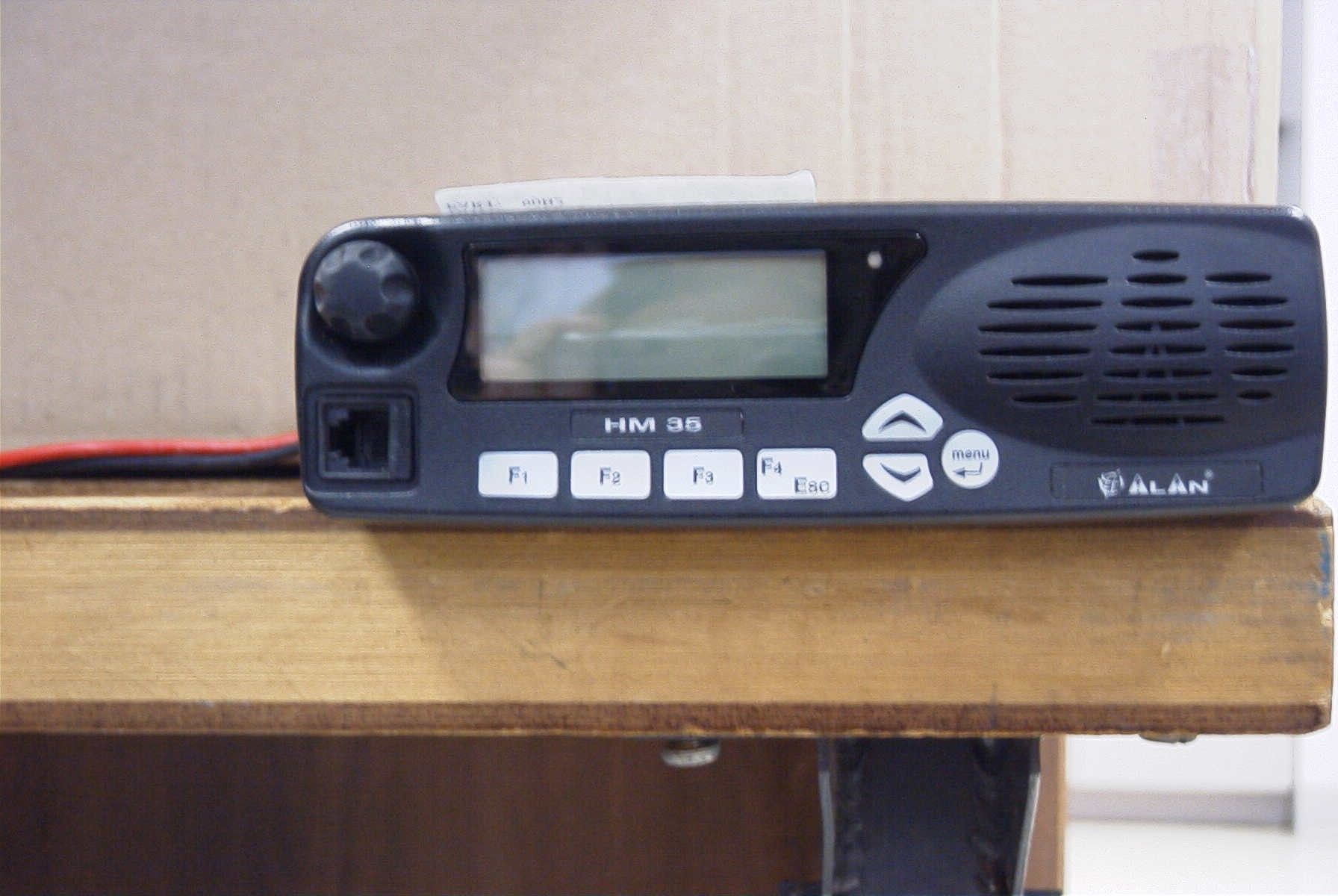
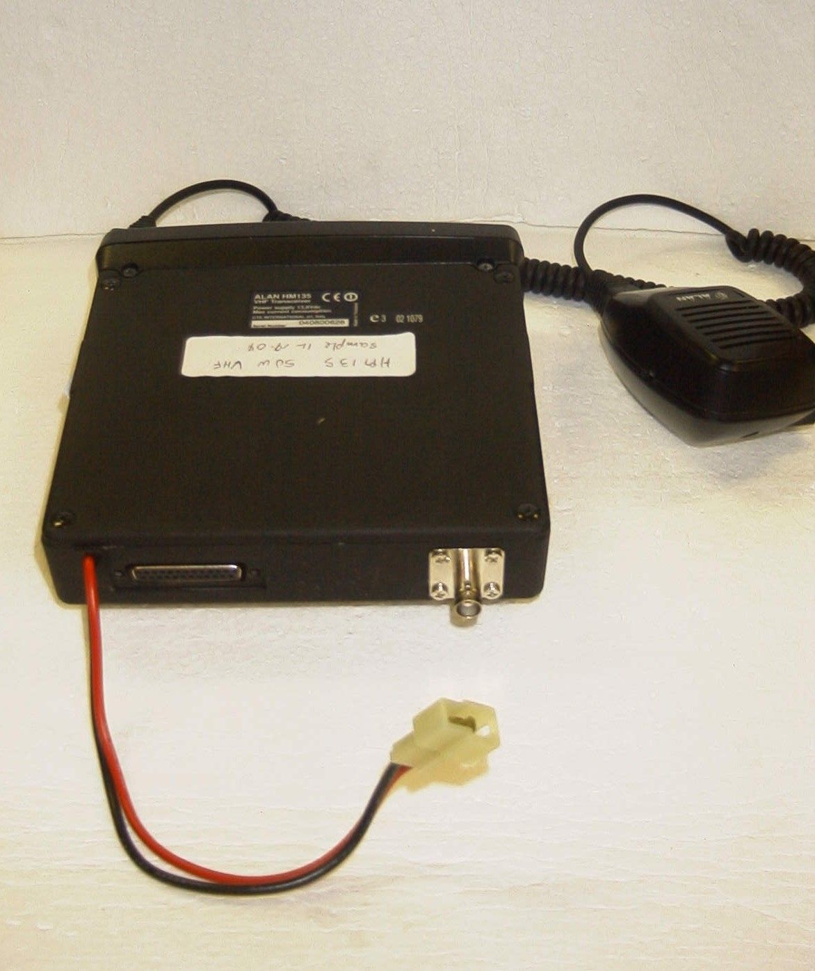
- VHF MOBILE TRANSCEIVER
- Frequency Range
- 136.00000000 - 174.00000000
- Company
- Midland Radio Corporation
- Country
- United States
Documents & Files
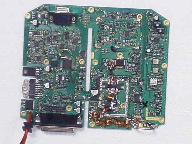
Document Text
Text extracted from the exhibit documents filed with the FCC. Open a document above to read the original.
Users Manual
70-3350/5445 – User’s Manual Midland Model 70-3350 Vehicular VHF Transceiver Model 70-5445 Vehicular UHF Transceiver User’s Manual Copyright © 2004 by Midland Radio Corporation; all rights reserved. This device complies with part 15 of the FCC Rules Operation is subject to the following two conditions: 1. This device may not cause harmful interference, and 2. This device must accept any interference received, including interference that may cause undesired operation. Rev. 0.1 on 27 December 2004 Page 1 of 32 70-3350/5445 – User’s Manual FCC RF EXPOSURE The FCC has adopted a safety standard for human exposure to RF energy. Proper operation of this radio under normal conditions results in user exposure to RF energy below the Occupational Safety and Health Act and Federal Communication Commission limits. Mandatory Safety Instructions to Installers and Users: This radio is NOT approved for use by the general population in an uncontrolled environment. This radio is restricted to occupational use and work related operations only. Radio operators must have the knowledge to control their exposure conditions and the exposure conditions of bystanders and/or passengers to satisfy the lower exposure limit allowed for General Population. To comply with FCC RF exposure limits, DO NOT operate the transmitter of this mobile radio when a person outside the vehicle is within 130 centimeters (51 inches) for VHF or 93 centimeters (37 inches) for UHF, of the antenna. The antenna supplied by the manufacturer or radio dealer must be mounted at a location such that during radio transmission, no person or persons can come closer than the above indicated minimum safe distance to the antenna, i.e. 130 or 93 cm. To comply with current FCC RF exposure limits, the antenna must be installed at or exceeding the minimum safe distance stated above, and in accordance with the requirements of the antenna manufacturer or supplier. Vehicle Installation Instructions: The antenna used for this transmitter must be mounted on the center of the roof ONLY and must be installed in vehicle having the following characteristics in order to prevent bystanders and passengers from being exposed to levels exceeding the limits for General Population/Uncontrolled Exposure environment: All passengers must be sitting under a solid metal roof. Rooftop width must be at least 76 inches OR the edges of the physical boundary of the vehicle must be at least 76 inches apart. DO NOT operate the radio without the proper antenna installed. Do not substitute any antenna for the one supplied or recommended by the manufacturer or radio dealer. The antenna gain must not exceed 0 dBd. By not following the antenna recommendations you may be exposing person(s) to excess radio frequency radiation. You may contact your radio dealer or the manufacturer for further instructions. DO NOT transmit more than 50% of total radio use time (50% duty cycle). Transmitting for more than 50% of the time can cause FCC RF exposure compliance requirements to be exceeded. This radio is transmitting whenever the TX icon is displayed on the LCD. Pressing the PTT switch on the side of the microphone normally causes the radio to transmit. Note: The preceding information is provided to make you aware of RF exposure and how to ensure that this radio is operated within FCC RF exposure limits. You, as the qualified end-user of this radio device must control the exposure conditions of bystanders to ensure the minimum separation distance, stated above for satisfying FCC RF exposure compliance, is maintained between the antenna and nearby persons. Transmit only when all person(s) are at least the minimum distance from the properly installed, externally mounted antenna. IMPORTANT SAFETY INFORMATION CAUTIONS The antenna connector must be snugly tightened to maintain proper electrical connection and moisture resistance. Equipment must be grounded according to Midland Radio Corporation installation instructions for safe operation. Equipment should be serviced only by a qualified technician. Refer to radio service manual for additional information on installation and safety precautions. WARNING! ! DO NOT allow the antenna to touch or come in very close proximity with the eyes, face, or any exposed body parts while the radio is transmitting ! DO NOT operate the radio in explosive or flammable atmospheres. The transmitted radio energy could trigger blasting caps or cause an explosion. ! DO NOT allow children to operate or play with this radio. Note: The above warning list is not intended to include all hazards that may be encountered when using this radio. Rev. 0.1 on 27 December 2004 Page 2 of 32 70-3350/5445 – User’s Manual In this manual... 1 GENERAL INFORMATION FOR THE HM35 SERIES....................................................................................5 2 ABOVE ALL... SAFETY!................................................................................................................................6 2.1 Conventions and Symbols Used in This Manual...........................................................................................................6 2.2 Warnings.......................................................................................................................................................................6 2.3 Security.........................................................................................................................................................................6 2.3.a General precautions.........................................................................................................................................6 2.3.b Operating conditions/usage..............................................................................................................................6 2.3.c Installation........................................................................................................................................…
Text truncated - open the document above for the full version.
Operational Description
HM135 Service Manual Preliminary version Page 4 of 13 2 CIRCUIT DESCRIPTION 2.1 General information The HM135 is basically divided into 2 printed circuit boards: Main board and Head. Circuitry and signals can be divided in the following sections: Microprocessor/control Front panel (head) circuitry VCO / Synthesizer (PLL) Transmitter Receiver Errore. L'origine riferimento non è stata trovata. ON/OFF switch, rear connector and internal connectors Refer to the Block Diagram and the Schematics. 2.2 Microprocessor/control The microprocessor DD5 is constantly operating when the radio is turned ON. It is continuously monitoring the keyboard, the PTT line and other internal inputs such as the squelch detect, etc. When a change occurs, the microprocessor makes the appropriate response according to its program in order to control the all radio functions. On channel change, the Radio emits a beep and the synthesizer is loaded with the correct frequency information. The microprocessor runs off a 8 MHz oscillator which is composed of X3, C353, C354 and R319. When the radio is first turned on, the microprocessor reads the radio status from the EEPROM DD3 which contains all the radio’s parameters. The microprocessor determinates the receive frequency codes, then loads the synthesizer via its pins 42 (line PLL_LE), 43 (line PLL_DATA) and 46 (line PPL_CLK). Pin 40 outputs a PWM signal which is converted by DA18:B into a CC voltage at its output (line RF_PWR_CTRL) which controls the RF output power. Pins 37 and pin 39 outputs a PWM signal which are used, respectively, to generate the Selcall signal (line MCU_SELCALL_PWM) and CTCSS/DCS signal (line MCU_CTCSS_DCS_PWM) as further explained. The digital signals coming from the ADC converters which drive the microprocessor in order to decode the Selcall and CXTCSS/DCS signals are applied, respectively, to pin 59 (line ADC_HI_SPEED_DATA_RX) and pin 60 (ADC_lo_SPEED_DATA_RX). The firmware program interface is made by means of the connector XP3 The microprocessor is fitted with an internal program flash memory as well, therefore functions can be customized, if necessary, upon specific request from the customer. 2.2.a PTT circuit The PTT switching is totally controlled by the two microprocessors (DD5 in the main board and DD800 in the front board in the front panel): when the PTT is pressed, the line AUX_PTT goes low, so the transistor VT806 changes the status of the pin 20 of microprocessor DD800 which is “informed” that the radio is in TX mode (i.e. PTT is pressed), so it changes its output at pin 22 putting the low level at pin 8 of the connector XT802 which is connected to the main PCB with the connector XT2. This means that pin 8 of XT2 (line HANDSET_PTT_TO_MPU) goes low. This line is connected to the VT56 which changes the status of pin 26 of the microprocessor DD5 from hi to low. Now the microprocessor DD5 is also “informed” that the radio is in TX mode, so it can control the +8V voltage which is alternatively fed to the TX or RX stages according to the radio’s status. Pins 29 (line TX_FROM_MCU) and 30 (line RX_FROM_MCU) control the +8V power switches which alternatively outputs this voltage to the RX section (line +8V_RX) with VT42 or to the TX one (line +8V_TX) with VT41. The transistor VT805 is controlled by the pin 19 of the microprocessor DD800 and it is used to eventually disable all the over stated PTT chain according to the radio’s status (e.g. busy lock out, timeout timer etc). HM135 Service Manual Preliminary version Page 5 of 13 2.3 Front panel (head) circuitry The microprocessor DD800 runs off a 8 MHz oscillator which is composed of X800, and R829. DD800 is basically used to control the LCD unit XT80, to decode the commands coming from the front keypad S801 to S808) as well as to switch the front LEDs DA800. It is also used to light up the LCD backlight (VD800 to VD805) as well as for the PTT circuit as over stated. The negative voltage necessary for the LCD is created by a charge pump which consists of VT815, VT813, VT812, VD809 and VD808. The output (line –8V) is fed to the regulator DA804:A which outputs the line VD in order to supply the LCD unit. The hang-up functions work this way: the line AUX_HOOK is connected to the microphone’s hook and it’s normally grounded (microphone hooked). When the mike is removed from its hook, the line AUX_HOOK changes its state driving the transistor VT809. This changes the status of the pin 21 of the microprocessor DD800 which opens the monitor through a command sent to the main microprocessor DD5 through a serial command. 2.4 VCO / Synthesizer (PLL) This section basically consists of the Temperature-Compensated Crystal Oscillator (TCXO), Voltage Controlled Oscillators (VCOs), Synthesizer and the Loop Filter. 2.4.a Temperature-Compensated Crystal Oscillator (TCXO) The reference oscillator is composed by the temperature compensated crystal X2 and related circuitry (DA1:A. VD19, VD20, VT21 and VT20), RP2 is used to adjust the oscillator on frequency (12.8 MHz) at room temperature. The reference oscillator is held within the specifications ±5 ppm from -25 to +55°C. 2.4.b Voltage-Controlled Oscillators The receive VCO consists of VT11, CV1, VD6 and VD9. This VCO oscillates at 45.1 MHz above the programmed receive frequency (i.e. from 181.1 to 219.1 MHz for the 135-174 MHz range). The VCO’s oscillating frequency is tuned by the varactors VD6 and VD9. The transmitter VCO consists of VT17, CV2, VD11-VD12 and VD13-VD14 and oscillates directly to the TX carrier frequency range (i.e. from 135 to 174 MHz range). The TX VCO is directly frequency-modulated by means of the varactor VD15 which is driven by the modulating signal (line A) regulated by the trimmer RP4. This is part of the double-point modulation and works mainly in high AF modulating frequencies), the other part of the double point- modulation is explained in the par. “Transmitter Audio Circuits”. The tuning voltage for the VCOs is supplied from…
Text truncated - open the document above for the full version.
Parts List/Tune Up Info
DEVELOPMENT : FINAL P A R T S L I S T # RIR610B DESIGN : FINAL =================== TECHNIQUE : FINAL R ev.: 033 S/W VERSION : UNDEFINED MODEL CODE : 7760 HM-135 VHF MOBILE LMR ( ) 4/01/28 7:33 2 1 ------ - - ---- ------------ -------------------- ------------------------------- -------- --- -- ---- ----------------------------------- -- -------- --- ---------- SEQ LEVEL PART-NO. NAME & DESCRIPTION Q'TY UT G KON REFERENCE-NO ECO-DATE ECO-NO. ------ - - ---- ------------ -------------------- ------------------------------- -------- --- -- ---- ----------------------------------- -- -------- --- ---------- 1 2 577-60C-A COVER ASS'Y 1 EA A 7/3/2015 A CT03-PAT 3 Nr 33 in DWG (+)MACHINE SCREW(BH) (Main PCB fix ) M3x6 ZN-PLAT (+) MA 13 EA B SUB 12/3/2008 A CT03-1289 3 Nr 34 in DWG (+)MACHINE SCREW(BH) (Power amp & 7808) M3X8 (+)BH NI 3 EA B SUB 12/3/2008 A CT03-1289 Nr 39 in DWG (+)MACHINE SCREW(BH) (Audio Amp) M3X6 (+)BH NI 1 Nr 36 in DWG WASHER SPRING (Power amp & 7808) Washer Spring 3.0mm Zn 3 3 Nr 14 in DWG (+)MACHINE SCREW(BH) (ESC + Main) M3X8 (+)PH BLK 4 EA B SUB 12/3/2008 A CT03-1289 3 Nr 37 in DWG (+)MACHINE SCREW(BH) (UHF Connector) M3X12 ZN-PLAT 2 EA B SUB 12/3/2008 A CT03-1289 3 Nr 36 in DWG (+)MACHINE SCREW(PH) ( UHF Connector) M3X5 (+)PH BLK 2 EA B SUB 12/3/2008 A CT03-1289 3 Nr 32 in DWG (+)MACHINE SCREW(BH) 4X10 BLK (+)PH MA 4 EA B SUB 1/4/2014 C CT04-0041 3 651-024 NUT SS41 M3-1S ZN-PLAT 2 EA B SUB 12/3/2008 A CT03-1289 3 702-491 BODY MAIN ALDC12 1 EA B SUB 7/3/2015 A CT03-PAT 3 71A-256 COVER MAIN ALDC12 1 EA B SUB 7/3/2015 A CT03-PAT 3 772-651 SHIELD UHF TIN 0.3 1 EA B SUB 8/3/2001 A CT03-PAT 3 772-652 SHIELD VCO TIN 0.3 1 EA B SUB 8/3/2001 A CT03-PAT 3 772-670-A SHIELD CAN STPE T0.15 1 EA B SUB 12/3/2015 A CT03-1330 3 896-252 GASKET BODY CONDUCTIVE RUBBER 1 EA B SUB 8/3/2001 A CT03-PAT 3 896-253 GASKET CABLE CONDUCTIVE RUBBER 1 EA B SUB 8/3/2001 A CT03-PAT 3 896-254 GASKET DB25 CONDUCTIVE RUBBER 1 EA B SUB 8/3/2001 A CT03-PAT 3 896-256 GASKET UHF CONDUCTIVE RUBBER 1 EA B SUB 8/3/2001 A CT03-PAT 3 896-325 GASKET DB9 SILICONE RUBBER BLK 1 EA B SUB 12/3/2017 A CT03-1332 896-044 SPONGE ( display module) 2 2 577-60E-A ESCUTCHEON ASS'Y 1 EA A 7/3/2015 A CT03-PAT 3 Nr 11 and 25 in DW G PT (+)TAPPING SCREW(PH) (PCB and Speaker) 2.5 X6 6 EA B SUB 12/3/2008 A CT03-1289 3 Nr 15 in DWG PT (+)TAPPING SCREW(PH) 2.5 X10 7 EA B SUB 12/3/2008 A CT03-1289 3 71A-257 HOUSING FRONT ALDC12 1 EA B SUB 7/3/2015 A CT03-PAT 3 796-017 OVERLAY PC TEXTURE T0.5 1 EA B SUB 12/3/2015 A CT03-1331 3 796-018 PLATE ALAN PC TEXTURE T0.5 1 EA B SUB 12/3/2015 A CT03-1331 3 801-817 E.S.C PC 1 EA B SUB 7/3/2015 A CT03-PAT 3 814-519 WINDOW ACRYL 1 EA B SUB 7/3/2022 A CT03-PAT 3 819-001 ILLUMINATOR ACRYL 1 EA B SUB 7/3/2015 A CT03-PAT 3 826-612 KNOB SILICONE RUBBER BLK 1 EA B SUB 7/3/2022 A CT03-PAT 3 896-216 KEY PAD SILICONE RUBBER 1 EA B SUB 7/3/2015 A CT03-PAT 3 896-255 GASKET FRONT CONDUCTIVE RUBBER 1 EA B SUB 8/3/2001 A CT03-PAT 3 896-326 GASKET SPEAKER SILICONE RUBBER BLK 1 EA B SUB 12/3/2017 A CT03-1332 3 2 577-60H-MA HEAD MANUAL ASS'Y 1 EA A 5/3/2027 A CT03-PAT 3 251-327-8 LED DUAL LAMP SPR-39MVW 1 EA B SUB DA800 6/3/1930 A CT03-KATHI 3 252-310-7 LCD MODULE PS12032LRS-DAN-K01 1 EA B SUB 9/3/2003 C AT03-PAT 3 270-359-8Z CERAMIC RESONATOR ZTT-8.00MT(8MHZ) 1 EA B SUB X800 9/3/2027 C CT03-1006 3 420-132-6 SPEAKER FB-064-A3123 4 OHM NOM 4.0W 1 EA B SUB 6/3/2019 A CT03-KATHI 3 420-863-3 JACK MODULAR 8949-F66/15 1 EA B SUB XT901 6/3/1930 A CT03-KATHI 3 CONN. DB9 STRIGHT ZDEE9S-OL2-146 1 EA B SUB XT802 11/3/2008 C CT03-1180 3 436-057-5 SW TACT SKQYAB 7 EA B SUB SB1.2.3.4.5.6.7 6/3/2020 C CT03-KATHI 4 2 577-60H-PB HAED POT. METER B'D 1 EA A 5/3/2027 A CT03-PAT 3 05B-103-5Z CHIP RESISTOR 10K 1/16W 5% T 1608 2 EA B SMD R901.902 6/3/2019 A CT03-KATHI 3 132-260-8Y CHIP CERAMIC 220PF GRM39 COG221J 50V PT 7 EA B SMD C901.902.903.904.905.906.907 6/3/2019 A CT03-KATHI 3 421-405-4 CONNECTOR FPC 8X1MM SMD TOP CONTACT(487951) 1 EA B SUB XT902 12/3/2024 C AT03-PAT 3 450-459-2 VR 10KA:PK093VS-1 15SK A10K 1 EA B SUB RP901 1/4/2005 C CT04-0007 5 2 577-60H-SA HEAD SMD ASS'Y 1 EA A 5/3/2027 A CT03-PAT 3 05B-101-3Z CHIP RESISTOR 100 1/16W 5% T 1608 4 EA B SMD R814.827.832.836 6/3/2019 A CT03-KATHI 3 05B-102-4Z CHIP RESISTOR 1K 1/16W 5% T 1608 4 EA B SMD R822.829.830.861 12/3/2012 C CT03-1307 3 05B-103-5Z CHIP RESISTOR 10K 1/16W 5% T 1608 27 EA B SMD R801.802.805.806.807.810.813. 12/3/2012 C CT03-1307 816.817.821.824.828.831.833. +840.842.844.850.851.852.853.855.856.857.858.860.854 3 05B-153-0Z CHIP RESISTOR 15K 1/16W 5% T 1608 9 EA B SMD R834.835.837.838.839.841.843. 6/3/2019 A CT03-KATHI 845.848 3 05B-154-1Z CHIP RESISTOR 150K 1/16W 5% T 1608 1 EA B SMD R808 12/3/2012 C CT03-1307 3 05B-222-9Z CHIP RESISTOR 2.2K 1/16W 5% T 1608 3 EA B SMD R819.820.862 6/3/2019 A CT03-KATHI 3 05B-223-0Z CHIP RESISTOR 22K 1/16W 5% T 1608 4 EA B SMD R823.825.864.866 12/3/2012 C CT03-1307 3 05B-272-4Z CHIP RESISTOR 2.7K 1/16W 5% T 1608 2 EA B SMD R811.812 6/3/2019 A CT03-KATHI 3 05B-472-8Z CHIP RESISTOR 4.7K 1/16W 5% T 1608 1 EA B SMD R815 6/3/2019 A CT03-KATHI 3 05B-473-9Z CHIP RESISTOR 47K 1/16W 5% T 1608 3 EA B SMD R847.859.863 1/4/2015 C CT04-0050 3 06J-101-6 CHIP RESISTOR 100 1/ 4W 5% T 3216 4 EA B SMD R800.803.846.849 7/3/2001 C CT03-KATHI 3 060-202-4Z CHIP RESISTOR 2K 1/10W 5% T 2012 1 EA B SMD R826 6/3/2019 A CT03-KATHI 3 060-221-1Z CHIP RESISTOR 220 1/10W 5% T 2012 2 EA B SMD R804.809 6/3/2019 A CT03-KATHI 3 130-A75-8Y CHIP CERAMIC 0.001UF GRM39 X7R102K 50V PT 5 EA B SMD C802.803.804.806.808.825 6/3/2019 A CT03-KATHI 3 130-B09-9Y CHIP CERAMIC 0.1UF GRM39 X7R104K 16V AT 8 EA B SMD C811.812.813.816.817.820.822. 6/3/2019 A CT03-KATHI 824 3 130-290-5Y CHIP CERAMIC 0.22UF GRM40 X7R224K 16V 1 EA B SMD C801 6/3/2019 A CT03-KATHI 3 131-089-7Y CHIP CERAMIC 1UF GRM40 Y5V105Z 16V PT 3 EA B SMD C805.821.823 6/3/2019 A CT03-KATHI 3 131-093-9Y CHIP CERAMIC 100PF GRM39 COG101J 50V PT 3 EA B SMD C800.807.818 6/3/2019 A CT03-KATHI 3 141-021-8 CHIP TANTALUM 10UF ECS…
Text truncated - open the document above for the full version.
Parts List/Tune Up Info
HM135 Service Manual Preliminary version Page 10 of 13 3 ADJUSTMENTS 3.1 General Adjustment trimmer potentiometer/capacitors in the HM135 main unit: Ref. Designator Used for... RP1 Squelch Level Adj. RP2 Frequency Adj. RP3 Deviation Balance ( Reference Oscillator Modulation Level) RP4 Maximum Deviation Adj. RP5 Transmitter Driver Bias Adj. RP6 Transmitter Power Amplifier Bias Adj. RP7 Transmitter Maximum Power Adj. CV1 Receiver VCO Adj. CV2 Transmitter VCO Adj. 3.2 Initial Settings , DO NOT CONNECT THE RADIO TO THE POWER SUPPLY BEFORE AND DURING INITIAL SETTINGS OF CONTROLS. 1) Connect an ohmmeter between the wiper of RP3 and Ground. Turn RP3 in CCW direction until readings of the ohmmeter are within 100 to 500 Ohm 2) Connect an ohmmeter between the wiper of RP5 and Ground. Turn RP5 in CCW direction until readings of the ohmmeter are within 100 to 300 Ohm 3) Connect an ohmmeter between the wiper of RP6 and Ground. Turn RP6 in CCW direction until readings of the ohmmeter are within 100 to 300 Ohm 4) Connect an ohmmeter between the wiper of RP7 and Ground. Turn RP7 in CCW direction until readings of the ohmmeter are within 200 to 500 Ohm 3.3 Applying power for the first time. , RF Power amplifier and AF Power Amplifier of the radio are connected to the power supply before the internal ON/OFF Switch, i.e. supply voltage is present even if the ON/OFF Switch is in OFF position. It is strongly recommended to disconnect the radio from the plus of the power supply if full switching OFF is needed. , Keep the minus of the Power Supply Unit connected to the GROUND. , Use pre-programmed and checked Front Panel. Control Function Initial Settings RP1 Squelch Level Adj. Center RP2 Frequency Adj. Center RP3 Deviation Balance Minimum (CCW), see note1. RP4 Maximum Deviation Adj. Center RP5 Transmitter Driver Bias Adj. Minimum, see note 2 RP6 Transmitter Power Amplifier Bias Adj. Minimum, see note 3 RP7 Transmitter Maximum Power Adj. Minimum, see note 4 CV1 Receiver VCO Adj. As is CV2 Transmitter VCO Adj. As is HM135 Service Manual Preliminary version Page 11 of 13 , Radio contains a number of ESD, most sensitive components, without build-in protection are LDMOS RF Power transistors. 1) Check connection between the Front Panel and the Main Unit. 2) Set ON/OFF Volume Potentiometer of the Front Panel Fully CCW (Switched Off) 3) Connect the radio’s Antenna connector to a Communication Tester, preset in Transmitter Measurement mode. 4) Set a Regulated Power Supply unit, capable to deliver at least 7A of DC Current, to 13.2V and current limit to 1A. 5) Connect the radio to the Power Supply Unit. Check the current. It must be below 30mA. 6) Switch ON the radio. Check the current, it must be below 0.5A. 7) Check Radio’s Internal Power Supply as follows: Between pin 1 of DA7 (KIA7808API) (the pin, nearest to the Audio Amplifier IC) and ground – plus 13.2V Between pin 3 of DA7 and ground – between 7.6 and 8.4V Between the positive electrode of C247 and ground - between plus 4.75 and 5.25V Between the positive electrode of C358 (near pin 1 of uP DD5) and ground plus 3.3, plus/minus 0.15V. 8) Switch off the radio. 3.4 Loading the Firmware 1) Connect a Firmware Programmer to the XP3, JTAG Connector. 2) Power On the radio 3) Load the firmware 4) Power Off the radio 5) Disconnect the Programmer. 6) Switch ON the Radio. Usually it will respond with BAD CRC Message on LCD. It is OK. Switch OFF the Radio. 3.5 Programming the radio 1) Connect the programming cable to radio’s Microphone Connector. 2) Press the F1 key, keep it pressed and switch ON the radio. Radio will respond with Programming... on the LCD and Orange light of front panel diode. Release F1 Key. 3) Program the radio using Factorytest1.hpv settings file. It includes 6 channels: CH1 - 135.100 MHz, 25 KHz Channel spacing, No CTCSS , No DCS, No Sellcall CH2 - 155.100 MHz, another settings as per CH1 CH3 - 173.900 MHz, another settings are as per CH1 CH4 - 135.100 MHz, 12.5 KHz Channel spacing, No CTCSS , No DCS, No Sellcall CH5 - 155.100 MHz, another settings as per CH 4 CH6 - 173.900 MHz, another settings are as per CH 4 CH7 - 155.1 MHz, 25 KHz spacing, CTCSS 67Hz on RX ant TX. CH8 - 155.1 MHz, 25 KHz spacing, CTCSS 254.1 Hz. CH9 - 155.1 MHz 25 KHz spacing , SELLCALL CCIR 12345 both RX ant TX 4) Switch OFF the radio and disconnect the programming cable. 5) Connect the microphone to the radio. 3.6 Setting the Power Amplifier Bias 1) Connect TP1, VCO voltage test point, to the ground. 2) Connect a 200 to 330 pF Disc Capacitor between the common point of VD16, VD17 and R98 and the ground. 3) Power ON the Radio. Push the PTT of the Microphone. 4) Note the current , it must be approx 400 to 500mA. 5) Turn slowly the RP5, TX Driver Bias in CW direction until the current from power supply is increased with approx. 300 mA. Note the current. 6) Turn slowly RP6, TXPA Bias in CW direction until the current is increased with approx. 300mA. Keep the current absolute value below 1.1 A. HM135 Service Manual Preliminary version Page 12 of 13 7) Release the PTT. 8) Power Off the radio. Disconnect the short from TP1. Keep the capacitor (step 2 above) connected. 3.7 Setting the frequency and VCO’s tuning. 1) Switch the radio ON 2) Go to CH3 (173.9 MHz) 3) Connect an oscilloscope between TP1 , located in the center of VCO shield, and ground. Turn CV1, RX VCO ADJ, slowly until the voltage at TP1 is between 6.5 and 7.1VDC, without notable ripple. 4) Press the PTT. Turn CV2 TX VCO ADJ slowly until the voltage at TP1 is between 6.5 and 7.1 VDC, without notable ripple. Release the PTT 5) Switch to CH1 (135.1 MHz). The voltage at TP1 must drop to 1.8 to 3V. Press the PTT. The voltage must be within 2 and 3.1V. 6) Repeat all above, if necessary. 7) Remove the 300pF capacitor (step 2 of the paragraph “Setting the Power Amplifier Bias” above). 8) Switch to CH2 (155 MHz). 9) Go to transmit (PTT) and turn slowly RP7, maximum TX Power until the output power is reached…
Text truncated - open the document above for the full version.
Schematics
ALAN HM 135 ELECTRICAL DIAGRAMS HM135_HEAD_FEB_14_2004.SCH pdfMachine by BroadGun Software 12 13 14 D 5 6 7 B 10 8 9 C pdfMachine by BroadGun Software 5 6 7 B 12 13 14 D 1 2 3 A 1 2 3 A 10 8 9 C pdfMachine by BroadGun Software 1 2 3 4 8 A 1 2 3 4 8 A 5 6 7 B 10 8 9 C 5 6 7 B 1 2 3 4 8 A 5 6 7 B 1 2 3 A 12 13 14 D 1 2 3 4 8 A pdfMachine by BroadGun Software 10 8 9 C 5 6 7 B 1 2 3 A 5 6 7 B 12 13 14 D pdfMachine by BroadGun Software pdfMachine by BroadGun Software 1 2 3 4 8 A pdfMachine by BroadGun Software 5 6 7 B pdfMachine by BroadGun Software 5 6 7 B 10 8 9 C 1 2 3 A 12 13 14 D pdfMachine by BroadGun Software pdfMachine by BroadGun Software
Test Report
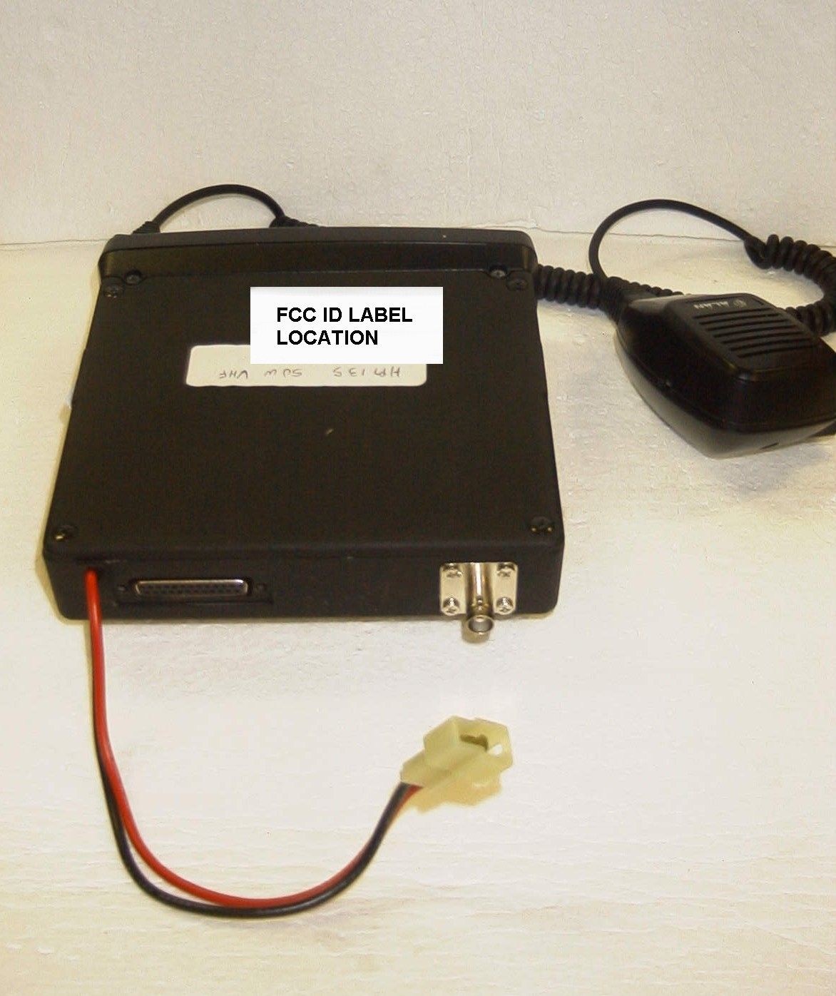
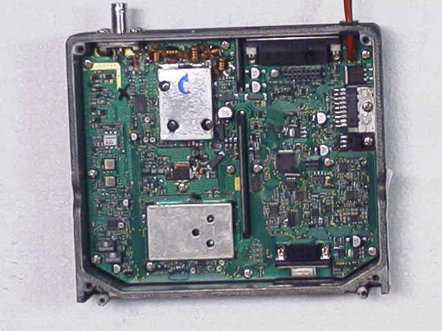
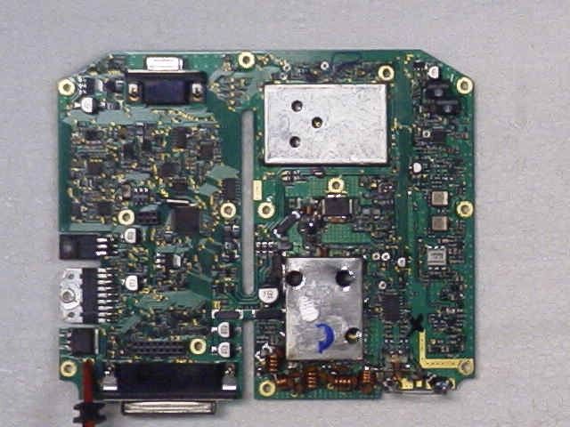
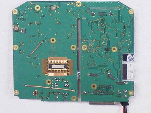
TIMCO ENGINEERING INC. 849 NW State Road 45 Newberry, Florida 32669 http://www.timcoengr.com 888.472.2424 F 352.472.2030 email: [email protected] APPLICANT: MIDLAND RADIO CORPORATION FCC ID: FCC Test Report Product Name: VHF MOBILE TRANSCEIVER FCC ID: MMA703350 Applicant: MIDLAND RADIO CORPORATION 1120 CLAY STREET NORTH KANSAS CITY MO. 64116 Date Receipt: NOVEMBER 30, 2004 Date Tested: DECEMBER 1, 2004 MMA703350 REPORT #: M\MidlandRadio_MMA\624YUT4\624YUT4TestReport.doc COVER SHEET TIMCO ENGINEERING INC. 849 NW State Road 45 Newberry, Florida 32669 http://www.timcoengr.com 888.472.2424 F 352.472.2030 email: [email protected] APPLICANT: MIDLAND RADIO CORPORATION FCC ID: APPLICANT: MIDLAND RADIO CORPORATION FCC ID: MMA703350 TABLE OF CONTENTS LIST TEST REPORT: PAGE 1...........GENERAL INFORMATION & TECHNICAL DESCRIPTION PAGE 2...........TECHNICAL DESCRIPTION CONTINUED RF POWER OUTPUT PAGE 3...........MODULATION CHARACTERISTICS AUDIO FREQUENCY RESPONSE PAGE 4...........MODULATION LIMITING PLOT PAGE 5...........AUDIO LOW PASS FILTER PAGE 6-8.........OCCUPIED BANDWIDTH PAGE 9...........SPURIOUS EMISSIONS AT ANTENNA TERMINALS PAGE 10..........METHOD OF MEASURING SPURIOUS EMISSIONS AT ANTENNA TERMINALS PAGE 11-13.......FIELD STRENGTH OF SPURIOUS EMISSIONS PAGE 14..........METHOD OF MEASURING RADIATED SPURIOUS EMISSIONS PAGE 15..........FREQUENCY STABILITY PAGE 16-17.......TRANSIENT FREQUENCY STABILITY PAGE 18-21.......TRANSIENT FREQUENCY RESPONSE PLOTS PAGE 22-27.......EQUIPMENT LIST EXHIBITS CONTAINING: BLOCK DIAGRAM SCHEMATIC PARTS LIST USERS MANUAL LABEL SAMPLE LABEL LOCATION EXTERNAL PHOTOGRAPHS INTERNAL PHOTOGRAPHS TUNING PROCEDURE OPERATIONAL DESCRIPTION TEST SET UP PHOTOGRAPH MMA703350 REPORT #: M\MidlandRadio_MMA\624YUT4\624YUT4TestReport.doc TABLE OF CONTENTS TIMCO ENGINEERING INC. 849 NW State Road 45 Newberry, Florida 32669 http://www.timcoengr.com 888.472.2424 F 352.472.2030 email: [email protected] APPLICANT: MIDLAND RADIO CORPORATION FCC ID: GENERAL INFORMATION REQUIRED FOR TYPE ACCEPTANCE 2.1033(c)(1)(2) MIDLAND RADIO CORPORATION will manufacture the FCCID: MMA703350 VHF TRANSCEIVER in quantity, for use under FCC RULES PART 90. MIDLAND RADIO CORPORATION 1120 CLAY STREET NORTH KANSAS CITY, MO. 64116 2.1033(c) TECHNICAL DESCRIPTION 2.1033(c)(3) Instruction book. A draft copy of the instruction manual is included in the exhibits. 2.1033(c)(4) Type of Emission: 8K9F3E 90.209 Bn = 2M + 2DK M = 2850 D = 1600 Bn = 2(2850) + 2(1600) = 8.9k 90.217 (b) Authorized Bandwidth 12.5 kHz 2.1033(c)(4) Type of Emission: 11K7F3E 90.209 Bn = 2M + 2DK M = 2850 D = 3000 Bn = 2(2850) + 2(3000) = 11.7k 90.217 (b) Authorized Bandwidth 25 kHz 2.1033(c)(5) Frequency Range: 136-174 MHz 90.209 2.1033(c)(6)(7) Power Output shall not exceed 59 Watts into a 50 ohm 90.205 resistive load. There are no user power controls. 2.1033(c)(8) DC Voltages and Current into Final Amplifier: POWER INPUT: FINAL AMPLIFIER ONLY INPUT POWER – HIGH: (13.8V)(5.17A) = 71.35 Watts INPUT POWER – LOW: (13.8V)(1.73A) = 23.87 Watts 2.1033(c)(9) Tune-up procedure. The tune-up procedure is included in the exhibits. MMA703350 REPORT #: M\MidlandRadio_MMA\624YUT4\624YUT4TestReport.doc Page 1 of 27 TIMCO ENGINEERING INC. 849 NW State Road 45 Newberry, Florida 32669 http://www.timcoengr.com 888.472.2424 F 352.472.2030 email: [email protected] APPLICANT: MIDLAND RADIO CORPORATION FCC ID: 2.1033(c)(10) Complete Circuit Diagrams: The circuit diagram and block diagram are included in the exhibits. (11) Function of each electron tube or semiconductor device or other active circuit device are in the exhibits. (12) Description of all circuitry and devices provided for determining and stabilizing frequency is included in the circuit description in the instruction manual. 2.1033(c)(13) A photograph or drawing of the equipment identification label is shown in the exhibits. 2.1033(c)(14) Photographs of the equipment of sufficient clarity to reveal equipment construction and layout and label location are shown in the exhibits. 2.1033(c)(15) Digital Modulation is not allowed. 2.1033(c)(16) The data required for 2.1046 through 2.1057 is submitted below. 2.1046(a) RF POWER OUTPUT RF power is measured by connecting a 50-ohm, resistive wattmeter to the RF output connector. With a nominal battery voltage of 13.8 VDC, and the transmitter properly adjusted the RF output measures: OUTPUT POWER: HIGH: 50 Watts LOW: 5 Watts Power Meter Transmitter under Test MMA703350 REPORT #: M\MidlandRadio_MMA\624YUT4\624YUT4TestReport.doc Page 2 of 27 TIMCO ENGINEERING INC. 849 NW State Road 45 Newberry, Florida 32669 http://www.timcoengr.com 888.472.2424 F 352.472.2030 email: [email protected] APPLICANT: MIDLAND RADIO CORPORATION FCC ID: 2.1047(a)(b) Modulation characteristics: AUDIO FREQUENCY RESPONSE The audio frequency response was measured in accordance with TIA/EIA Specification 603. The audio frequency response curve is shown below. The audio signal was fed into a dummy microphone circuit and into the microphone connector. The input required to produce 30 percent modulation level was measured. Audio Frequency Response Plot -5 +10 -2.5 +0 +2.5 +5 +7.5 d B 100 4k 200 300 400 500 700 1k 2k 3k Hz MMA703350 REPORT #: M\MidlandRadio_MMA\624YUT4\624YUT4TestReport.doc Page 3 of 27 TIMCO ENGINEERING INC. 849 NW State Road 45 Newberry, Florida…
Text truncated - open the document above for the full version.
Contact Information
Applicant
Butch Rittmann(Director of Operations)
Test Firm
Timco Engineering, Inc.S Sanders
Technical Specifications
| # | Rule Parts | Frequency Range | Power Output | Emission | Tolerance |
|---|---|---|---|---|---|
| 4 | 9 | 136 MHz - 174 MHz | 5 W | 11K7F3E | 2.5 ppm |
Other Applications from Midland Radio Corporation
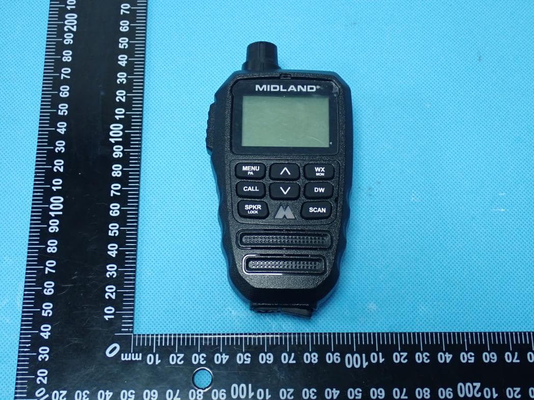
MMAMXMC95
Jun 10, 2026Wireless Bluetooth Microphone
Equipment Class
JAB - Part 15 Class B Digital Device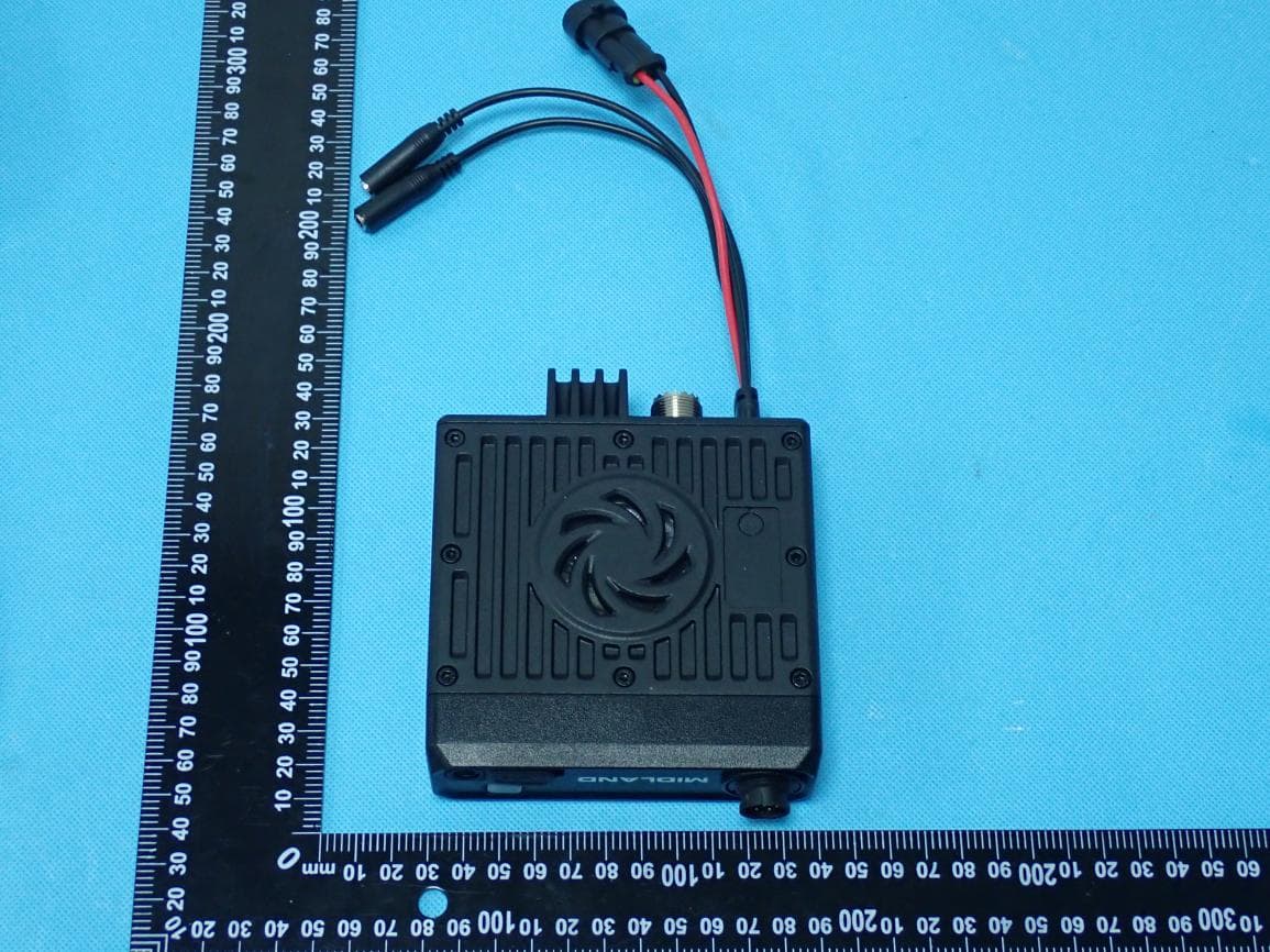
MMAMXT295
Jun 08, 2026GMRS Radio
Equipment Class
TNF - Licensed Non-Broadcast Transmitter Held to Face
MMACLIPTALK
Apr 27, 2026Transceiver
Equipment Class
DTS - Digital Transmission System
MMABR200S
Jan 13, 2026BUSINESS BAND TWO-WAY RADIO
Equipment Class
TNF - Licensed Non-Broadcast Transmitter Held to Face
MMAGXT67
Oct 29, 2023GMRS RADIO
Equipment Class
TNF - Licensed Non-Broadcast Transmitter Held to Face