MMA710110CLand Mobile Radio
Midland Radio Corporation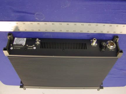
Click to zoom
Application Details
- Equipment Class
- TNB - Licensed Non-Broadcast Station Transmitter
- Date of Grant
- Jun 08, 2003
- Application Purpose
- Original Equipment
- Date of Application
- Jun 08, 2003
- Equipment Note
- Land Mobile Radio
- Frequency Range
- 40.00000000 - 50.00000000
- Company
- Midland Radio Corporation
- Country
- United States
Documents & Files
Document Text
Text extracted from the exhibit documents filed with the FCC. Open a document above to read the original.
Users Manual
OPERATOR'S MANUAL BASE TECH II BASE/REPEATER STATION 5/03 Midland Radio Corp. Base Tech II Base/Repeater Station Operator’s Manual 2 Introduction..................................................................................................................................................3 Description..............................................................................................................................................3 Features..................................................................................................................................................3 Controls, Indicators and Connectors......................................................................................................4 Operation......................................................................................................................................................7 Installation and Programming.................................................................................................................7 Basic Operation.......................................................................................................................................8 Front Panel Operation.............................................................................................................................9 Signaling............................................................................................................................................... 11 Scanning...............................................................................................................................................14 Locking the Keypad..............................................................................................................................17 Changing Tone Signaling Systems.......................................................................................................17 Displaying the Channel Information......................................................................................................18 Display of Received Tone Frequencies................................................................................................19 Bar Graph Displays...............................................................................................................................20 LCD Display Back Light........................................................................................................................20 Transmit Power Change.......................................................................................................................20 Calling Party ID Display........................................................................................................................21 Displaying any Radio's ID Number.......................................................................................................21 Emergency Caller Display.....................................................................................................................22 Automatic Transmit in Repeater Mode.................................................................................................22 TX Test Mode........................................................................................................................................23 Keypad Test Mode................................................................................................................................23 Frequency Band Test Mode..................................................................................................................24 Starting Message..................................................................................................................................24 Serial Number Display..........................................................................................................................24 EEROM Data Check Mode...................................................................................................................25 Hardware Error Detection.....................................................................................................................26 RS232C Communications Error............................................................................................................27 Base Tech II Base/Repeater Station Operator’s Manual 3 INTRODUCTION Description The Base Tech II Base Repeaters represents a technological advancement over previous models. The Base Tech II Base Repeater is comprised of separate modules all housed within one 2RU equipment cabinet. The receiver, transmitter, and PA unit are each enclosed within their own die-cast housing. Each one is then mounted directly on the large upper heatsink. A microprocessor-controlled interface module controls the channel selection, LCD Display, timers, interfaces, and signaling features. The RF power output is 25 — 110 watts, depending on the model, and rated for continuous duty. The CTCSS module supports all EIA tones. All tones and different encode and decode tones can be set on a per channel basis during radio programming. Attention The antenna(s) used for this transmitter must be fixed-mounted on outdoor permanent structures with a separation distance of at least 6 meters from all persons during normal operation. The peak conducted output power at each antenna terminal must not exceed 250 Watts and the peak radiated output power must not exceed 1000 Watts EIPR. Users and installers must ensure that FCC requirements for satisfying RF exposure compliance are met. (See FCC Rules Part 1, Sections 1307 and 1310) Features o Simplex or two frequency Duplex operation o EEPROM programmable with a PC computer o 99 programmable multi-mode channels o Full dot matrix LCD o Front-facing speaker o Transmit time limiter to prevent channel jamming o TX and RX encryption optional o Two channel scanning modes o 5-Tone encoder and decoder plu…
Text truncated - open the document above for the full version.
Block Diagram
2 2A-SA0042 KG510-30MHz 51BLK30Y RX UNIT CONTROL UNIT PA UNIT TX UNIT BLOCK DIAGRAM LOGIC UNIT PA section block diagram for 71-0110 (A,B, or C)
Block Diagram
PA section block diagram for 71-0110 (A,B, or C)
External Photos
Midland Radio Corporation FCC ID: MMA710110C APPENDIX C - EUT PHOTOGRAPHS Chassis - Front View Chassis – Rear View Midland Radio Corporation FCC ID: MMA710110C Chassis – Top View
ID Label/Location Info
APPENDIX A - FCC ID LABELING AND LOCATION Proposed FCC ID Labeling Proposed FCC ID Location Rear Side of EUT / Proposed Label Location FCC ID: MMA710110C
Internal Photos
Midland Radio Corporation FCC ID: MMA710110C EUT- Housing and Board Chassis – Cover Off Midland Radio Corporation FCC ID: MMA710110C EUT - Transmitter Component View EUT – Transmitter Solder View Midland Radio Corporation FCC ID: MMA710110C EUT – Receiver Component View EUT – Receiver Solder View Midland Radio Corporation FCC ID: MMA710110C DC Power Cable
Operational Description
Description 71-0110 © Midland Radio Corporation 12 CIRCUIT DESCRIPTION RECEIVER PART 1) RF section: An incoming signal is fed to pre-selector (BPF-101), and amplified by Q101, then fed to post-selector (BPF-102). The balanced mixer, consisting of T101, T102, D107 and D108, produces 21.6MHz by injection from the 1 st local signal provided by Rx. 2) Noise Blanking Section: The noise blanking circuit consists of Q102 (1 st noise amplifier), Q121 (buffer amplifier), Q122 (2 nd noise amplifier), Q123 (3 rd noise amplifier), Q125 (1 st pulse amplifier), Q104 (2 nd pulse amplifier), and a blanker switch formed by D103 through D106. An incoming signal is divided by the 1 st RF amplifier (Q101) to feed the 2 nd BPF and to feed the 1 st noise amplifier. A noise is amplified by Q102, Q121, Q122, Q123, Q125 and Q104. Then the amplified pulse triggers the blanker switch to eliminate the noise within the RF signal. 3) IF section: The output signal from the balanced mixer is fed to the crystal filters (XF101), then amplified by Q103. Again, this signal is fed to the 4-pole crystal filters and amplified by Q113. After being amplified by Q113, the signal is fed to 2 nd IF processor IC (IC106). The 2 nd local crystal oscillator signal is fed to IC106 to produce the 2 nd local signal (455KHz). IC106 amplifies the 2 nd local signal, which becomes an audio signal after the detector circuit included in IC106. Then, the audio signal is fed to the low-pass filter included in IC107, and fed to audio processor IC (IC3). 4) VCO section: The oscillator circuit formed by L303, D303, D305 and Q301 produces the 1 st local signal (Rx frequency plus 21.6MHz). The 1 st local signal is amplified by buffer amplifier Q302, and again amplified by pre- amplifier IC301 and post amplifier Q303. The amplified signal is fed to the balanced mixer. 5) PLL section: PLL IC with pre-scaler IC101 compares the phase between the VCO frequency and reference oscillator frequency (12.00MHz) by method of dividing the frequency, and produces VCO control signal. Then, this control signal is fed to the charge pump, consisting of Q108, Q109 and Q110, and fed to the LPF. The supply voltage of charge pump is multiplied by IC102 (approx. 15V) to achieve greater C/N ratio. TRANSMITTER PART 1) VCO section: The oscillator circuit formed by L303, D305 and D306 generates transmitter frequencies. Then this signal is fed to the 3-stage of amplifiers, buffer amplifier Q302, pre-amplifier IC301 and post amplifier Q303 and then to the final amplifier. 2) PLL section: Basically, the circuit description is the same as Rx. PLL IC with pre-scaler IC205 compares the phase between the VCO signal and reference oscillator frequency (12.00MHz) by method of dividing the frequency, and produces VCO control signal. Then this VCO control signal is fed to the charge pump, Description 71-0110 © Midland Radio Corporation 13 consisting of Q206, Q207 and Q208, and fed to the LPF. The supply voltage of charge pump is amplified by IC206 (approx. 15V) to achieve greater C/N ratio. 3) Modulator section: The modulation signal is fed to both VCO and the reference oscillator (TCXO); this permits very flat modulation characteristics against low frequency (DC). 4) TX Pre-amp section: The VCO signal is amplified by Q215 and Q216 to achieve 250mW. 5) PA section: The signal from pre-amp stage is fed to Q503 (driver) and Q504 and Q505 (final amplifiers) to achieve 110W output power. Then, signal is fed to the LPF to eliminate the harmonics spurious frequencies. An APC circuit formed by IC502, IC503, Q504 and Q505 stabilizes the output power at the set level. An IC501 protects Q504 and Q505 from the reverse power caused by the un-matched aerials. LOGIC PART 1) Microcomputer (CPU) section: A CPU, IC-1, uPD78F005 is the 8-bit processor with 60K flash memory and 2K RAM inside. This CPU controls all functions of the radio. A flash memory permits ON-BOARD-UP-GRADE when the new software is released. 2) EEPROM section: An IC7 is the 64kbit EEPROM. This IC contains all channel parameters 3) Audio processor section: IC2 is for TX and IC3 is for Rx audio processing. These IC’s control all audio processing and encode/decode CTCSS tones as commanded by the CPU. These IC’s also have a 2400bps MODEM to enable to form MPT1327 trunking protocols by using external MPT control software. FRONT CONTROL PANEL PART 1) LCD display section: LCD display is constructed by 128 x 32 dot matrix. This allows indication not only of characters but also graphics and symbols as designed. 2) LED display section: The 4 LED’s indicate modes of operation. 3) Audio amplifier section: IC404 has 2W audio power to drive the 8-ohm speaker mounted on the panel 4) Microphone pre-amplifier section: IC401 is the voice pre-amplifier having –34dBm output to feed the TX modulator. Description 71-0110 © Midland Radio Corporation 14 REMOTE CONTROL 25 pin D-sub connector for remote control is provided on the rear panel. The functions of each pin are as follows: Pin No. Name Description I/O Levels Comments 1 CH0 LSB external binary channel selection I 0-+5VDC 000000 is channel 1 2 CH1 External binary channel selection I 0-+5VDC 3 CH2 External binary channel selection I 0-+5VDC 4 CH3 External binary channel selection I 0-+5VDC 5 CH4 External binary channel selection I 0-+5VDC 6 CH5 MSB external binary channel selection I 0-+5VDC 7 GND 8 RSSI Receive signal strength indicator O 0-+2VDC analog 9 DISC OUT Discriminator audio out O ≈330mVrms 1KHz @ ±3KHz 10 SQ CONT Squelch control I 11 BUSY Channel busy indication O 0-+5VDC 5V=busy 12 MUTE External audio mute I 0-+5VDC 0V=muted 13 MOD1 External audio modulation input I ≈50mVrms 1Khz for ±3KHz 14 GND 15 PTT Push to talk I 0-+5VDC 0V=transmit 16 MOD2 External modulation input I ≈400mVrms 1KHz for ±3KHz After limiter and filtering 17 SIMP Simplex mode selected O 0-+5VDC 0V=simplex 18 ERR Alarm indication O 0-+5VDC 5V=alarm 19 DECODE Decode valid indication O 0-+5VDC 5V=valid signaling 20 RX AUD1 Buff…
Text truncated - open the document above for the full version.
Operational Description
General Information 71-0110 © Midland Radio Corporation 1 SPECIFICATIONS General Frequency Range: A Band: 30-40MHz B Band: 35-45MHz C Band: 40-50MHz * Number of Channels: 99 channels with name Channel Spacing: 12.5/20/25/30kHz Operation Mode: Simplex/Semi Duplex/Full Duplex Antenna Impedance: 50 ohm unbalanced Power Supply: DC 13.6V negative ground only Consumption: 18 amperes or less Environmental Conditions: -30 to +60 degree C, 95% humidity @35C Dimensions: 462 (w) 88 (h) 360 (d) mm Weight: 11 kgs. Transmitter Output Power: 60-110W continuous Switchable Bandwidth: Full sub band Frequency Deviation: ±5kHz(wide band) ±2.5kHz(narrow band) Frequency Stability: 2.5ppm Frequency Response: Within +1, -3dB, 300-3000Hz Signal to Noise Ratio: 50dB or more @1kHz 70% mod. (45dB at narrow) Modulation Distortion: 3% or less Spurious & Harmonics: 0.25μW or less Receiver Switchable Bandwidth: 3MHz IF Frequencies: 1 st IF 21.6MHz, 2 nd IF 455kHz Frequency Stability: 2.5ppm Sensitivity: 0.4μV or less for 20dB N.Q./ 0.3μV or less for 12dB SINAD Squelch Sensitivity: 0.25μV or less Selectivity: 70dB or more at 25kHz Blocking: 90dB or more Intermodulation: 70dB or more Spurious Response: 70dB or more AF Response: Within +1, -3dB, 300-3000Hz AF Distortion: 5% or less @1kHz 70% mod Signal to Noise Ratio: 50dB or more @1kHz 70% mod. (45dB at narrow) * Note: Band letter is the suffix of the model number. General Information 71-0110 © Midland Radio Corporation 2 OPTIONS & ACCESSORIES 70-RM-50M-BB .................................50 AMP Rackmount Power Supply w/Battery Back-up 70-RM-20M-BB.................................20 AMP Rackmount Power Supply w/Battery Back up 71-1480...........................................Programming Kit, Interface Cable & Software 70-8081...........................................Slide Rail for Power Supply 71-8082...........................................Slide Rails for TX/RX Unit 71-7801...........................................High Power Tx/Rx Antenna Relay (100 Watt Stations) 71-7751...........................................Low Power Tx/Rx Antenna Relay (50 – 60 Watt Stations) 71-8820A.........................................31 1/2” Indoor Cabinet, complete with locking doors. 71-8830A.........................................40 1/4” Indoor Cabinet, complete with locking doors. 71-8871...........................................12 1/4” Blank Panel 71-8870...........................................10 1/2” Blank Panel 71-8863...........................................3 1/2” Blank Panel 71-8862...........................................1 3/4” Blank Panel 71-0033...........................................DC Power Cable 71-8818........................................... TX RF Cable Kit (100 Watt) 71-2020...........................................10 Channel Tone Remote Termination with enclosure. 71-2021...........................................2 Channel DC Remote Termination with enclosure. General Information 71-0110 © Midland Radio Corporation 3 OPTIONS & ACCESSORIES 71-2022...........................................Microwave Interface with enclosure. 71-7206...........................................Tone Termination Lightning/Surge Protection. 71-ISSPTL.......................................DC Termination Lightning/Surge Protection. 71-7207...........................................AC Surge Protection Kit 71-7655A......................................... RF Line Arrestor 71-8880...........................................90” Aluminum Rack 71-8845...........................................67” Indoor Cabinet (Requires 71-8845-1Hardware Kit) 71-8845-1.........................................Mounting Hardware Kit for 71-8845Cabinet 71-8845-2.........................................Grounding Kit for 71-8845 Cabinet 71-8845-3.........................................Caster Kit for 71-8845 Cabinet 71-2315...........................................Palm Microphone 71-2316...........................................Desktop Microphone
Parts List/Tune Up Info
Preparation 71-0110 © Midland Radio Corporation 4 ALIGNMENT PROCEDURES RECEIVER PART 1) BPF-101 and BPF-102 alignment Connect the signal generator to the Rx antenna connector of the unit. Align the BPF-101 and BPF-102 to obtain the maximum sensitivity. For better alignment, if you have spectrum analyzer and tracking generator, connect the tracking generator to the Rx antenna connector and pick up the output signal from J101 to connect spectrum analyzer. Align the BPF-101 and BPF-102 to cover the desired bandwidth of receiving frequencies. 2) FVR101 alignment This is to adjust the tight squelch level. 3) VCO alignment The VCO has been aligned at the factory to cover full bandwidth. However, if you need to re-adjust the VCO when you repair, set the VCO voltage at 10.5V by L303 at the highest band frequency. TRANSMITTER PART 1) FVR201 alignment This potentiometer determines the modulation level. Carefully align FVR201 to obtain flat deviation from the lowest to the highest frequency installed in the transmitter. 2) FVR202 alignment This potentiometer determines the low frequency (below 300Hz) deviation. When CTCSS or DCS are used, it is necessary to align FVR202 to have enough deviation at low frequency. FVR204 FVR203 FVR202FVR201 3) FVR203 alignment FVR203 sets the maximum deviation, normally set at 5KHz. Also 2KHz or 2.5KHz deviation, for narrow spacing, can be selected with the programming software. 4) FVR204 alignment FVR204 adjusts the output power supplied to the transmitter. 5) VCO alignment The VCO has already been aligned at the factory, however if you need to re-adjust, set the VCO voltage to 10.5V at the highest band frequency. Preparation 71-0150 © Midland Radio Corporation 5 POWER AMPLIFIER PART 1) FVR505 Adjust FVR505 to gain the maximum efficiency as well as the maximum power output at the final transistor of the power amplifier. 2) FVR501 Adjust FVR501 for minimum reverse power when the antenna is terminated with 50 ohms load. 3) FVR502 FVR502 sets the point where reverse power is detected. 4) FVR503 FVR503 sets the point where a low-power-alarm is triggered. 5) FVR504 FVR504 sets the maximum power from the power module, however, do not exceed 70 watts. LOGIC PART FVR1 FVR2FVC1 FVR3 1) FVR1 alignment Set FVR1 to obtain 0dBm output into 600 ohms. 2) FVR2 alignment Adjust FVR2 for flat deviation level when used for a repeater. 3) FVR3 alignment FVR3 adjusts the power level indicator on the LCD. 6) FVC1 alignment Use FVC1 to shift the CPU clock frequency when necessary. A beat interference sometimes happens at certain frequency. In such case, shifting the CPU clock frequency may eliminate the interference. Preparation 71-0110 © Midland Radio Corporation 6 FRONT CONTROL PANEL PART FVR401 Hi FVR402 Lo VR401 VR402 FVR403 1) VR401 alignment This is a volume controller. 2) VR402 alignment This is a squelch level controller. 3) FVR401 alignment Use FVR401 to set the HI-POWER-LEVEL of the Tx output power. 4) FVR402 alignment Use FVR402 to set the LO-POWER-LEVEL of the Tx output power. 5) FVR403 alignment This is to set the contrast of the LCD back light.
Parts List/Tune Up Info
Parts List 71-0150 © Midland Radio Corporation 33 PARTS LIST Control Unit MISCELLANEOUS REF. # DESCRIPTION PART NUMBER CN405 CHIP CONN. 00-6200-510-130-000 70-159860 SWITCH SKHMPW 70-183160 P.C.B. 51KEY87-1(1/4) 70-070511 SPACER 4A10-2996 70-156162 SCREW SEMS SE-3 X 8 70-151229 P.C.B. 51VRS87-2(1/4) 70-070512 CN407 CHIP CONN. 00-6200-508-130-000 70-159885 D412 DIODE SLA-370MT-3F 70-085556 SW401 SWITCH SPPH23056A 70-183161 VR401 ROTARY SWITCH RY-6459 70-183162 VR402 ROTARY SWITCH RY-6460 70-183163 BUTTON 4A10-2988 70-110145 SCREW SEMS SE-3 X 10 70-151060 INTEGRATED CIRCUITS IC401 CHIP IC TA75S558F-TE85R 70-076921 IC402 CHIP IC TC74HC373AF(TP1) 70-076941 IC403 CHIP IC. TA78M05F-TE16L 70-076922 IC404 IC TA8201AK 70-076923 IC405 IC PQ12RH11 70-076924 IC406 CHIP IC NJU7662M-T1 70-076925 IC407 CHIP IC BU4S01-TR 70-076926 TRANSISTORS Q401 CHIP TR DTC114EKA-T146 70-080553 Q402 CHIP TR FMG9A-T148 70-080554 Q403 CHIP TR FMG9A-T148 70-080554 Q404 CHIP TR 2SD1766-T100 70-080555 Q405 CHIP TR 2SD2351-T106 70-080556 Q406 CHIP TR 2SJ503 70-080557 Q407 CHIP TR UMC2-TR 70-080558 Q408 CHIP TR 2SA1434-TB 70-080559 Q409 CHIP TR 2SA1434-TB 70-080559 Q410 CHIP TR 2SA1434-TB 70-080559 DIODES D405 CHIP DIODE 1SS355 70-085537 D406 CHIP DIODE 1SS355 70-085537 D407 CHIP DIODE 1SS355 70-085537 D408 CHIP DIODE 1SS355 70-085537 D409 CHIP DIODE 1SS355 70-085537 D411 CHIP DIODE DA204U-T106 70-085538 D412 CHIP DIODE DA204U-T106 70-085538 D414 CHIP DIODE 1SS355 70-085537 CAPACITORS C401 CHIP CAP 1nf 0805 50V 70-138810 C402 CHIP CAP 1μf 1206 50V 70-138838 C403 CHIP ELYC 1μf 10V 70-138850 C404 CHIP CAP 100pf 0805 50V 70-138380 C405 CHIP ELYC 10μF 16V 70-138852 C406 CHIP CAP 0.1μf 1206 50V 70-138837 C407 CHIP CAP 270pf 0805 50V 70-138384 C408 CHIP CAP 270pf 0805 50V 70-138384 C409 CHIP ELYC 10μf 16V 70-138852 C410 CHIP CAP 1nf 0805 50V 70-138810 C411 CHIP CAP 0.1μf 1206 50V 70-138837 C412 CHIP ELYC 10μf 16V 70-138852 C413 CHIP ELYC 10μf 16V 70-138852 C414 CHIP ELYC 10μf 16V 70-138852 C417 CHIP TANTALUM 1μf 1206 16V 70-138844 C418 C.ELYC 470μf 35V 70-138856 C419 C.ELYC 470μf 35V 70-138856 C420 C.ELYC 1000μf 16V 70-138857 C421 CHIP CAP 1nf 0805 50V 70-138810 C422 CHIP CAP 1μf 1206 50V 70-138838 C424 CHIP ELYC 47μf 16V 70-138854 C425 CHIP ELYC 4.7μf 25V 70-138851 C427 CHIP TANTALUM 10V 1206 70-138849 C428 C.ELYC 220μf 16V 70-138855 C429 CHIP CAP 0.1μf 0805 25v 70-138836 C430 CHIP CAP 0.1μf 0805 25v 70-138836 C431 CHIP CAP 0.1μf 0805 25v 70-138836 CONNECTORS CN401 MIC SOCKET 8 PIN 290A-88-30-119 70-159859 CN402 CHIP CONN. 20 PIN 00-6200-520-330-000 70-159871 CN403 CHIP CONN. 16 PIN 00-6200-516-230-000 70-159872 Parts List 71-0150 © Midland Radio Corporation 34 Control Unit (continued) CN404 CHIP CONN. 10 PIN 00-6200-510-130-000 70-159860 CN406 CHIP CONN. 8 PIN 00-6200-508-130-000 70-159885 CN408 CONNECTOR 3 PIN B 3P-VH 70-159861 CN409 CONNECTOR 2 PIN SB20-02WS 70-159862 CP401 CONNECTOR FF20-TAMEP1 70-159863 DIODES D401 LED MU16-4101 70-085539 D402 LED MU16-3101 70-085540 D403 LED MU16-2101 70-085541 D404 LED MU16-5101 70-085542 CABLES FC402 FLAT CABLE 4A-S429 70-033046 FC403 FLAT CABLE 4A-S471 70-033047 FC405 FLAT CABLE 4A-S585 70-033048 FC407 FLAT CABLE 4A-S584 70-033049 VARIABLE RESISTORS AND CAPACITORS FVR401 VR GF06P 10K 70-164177 FVR402 VR GF06P 100K 70-164178 FVR403 CHIP VARICAP EVM-7JSX30B14 70-123104 MISCELLANEOUS J401 HEADPHONE JACK S-G8022#01 70-153142 LD401 LCD TM12832BBC 70-202097 RESISTORS R401 CHIP RES. 0 ohm 1/10W 0805 70-144372 R405 CHIP RES. 15k ohm 1/10W 0805 70-144395 R406 CHIP RES. 1k ohm 1/10W 0805 70-144384 R407 CHIP RES. 10k ohm 1/10W 0805 70-144394 R408 CHIP RES. 27k ohm 1/10W 0805 70-144163 R409 CHIP RES. 100k ohm 1/10W 0805 70-144402 R410 CHIP RES. 100k ohm 1/10W 0805 70-144402 R411 CHIP RES. 47k ohm 1/10W 0805 70-144400 R412 CHIP RES. 2.2k ohm 1/10W 0805 70-144388 R414 CHIP RES. 2.2k ohm 1/10W 0805 70-144388 R415 CHIP RES. 56 ohm 1/10W 0805 70-144714 R416 CHIP RES. 56 ohm 1/10W 0805 70-144714 R417 CHIP RES. 220 ohm 1/10W 0805 70-144379 R418 CHIP RES. 33k ohm 1/10W 0805 70-144713 R419 CHIP RES. 47k ohm 1/10W 0805 70-144400 R420 CHIP RES. 18k ohm 1/10W 0805 70-144396 R421 CHIP RES. 8.2k ohm 1/10W 0805 70-144393 R422 CHIP RES. 47 ohm 1/10W 0805 70-144376 R423 CHIP RES. 47 ohm 1/10W 0805 70-144376 R424 CHIP RES. 22k ohm 1/10W 0805 70-144397 R425 CHIP RES. 4.7k ohm 1/10W 0805 70-144390 R426 CHIP RES. 4.7k ohm 1/10W 0805 70-144390 R427 CHIP RES. 180 ohm 1/10W 0805 70-144716 R428 CHIP RES. 47 ohm 1/10W 0805 70-144376 R429 CHIP RES. 47 ohm 1/10W 0805 70-144376 R430 CHIP RES. 4.7k ohm 1/10W 0805 70-144390 R431 CHIP RES. 4.7k ohm 1/10W 0805 70-144390 R432 CHIP RES. 4.7k ohm 1/10W 0805 70-144390 R433 CHIP RES. 4.7k ohm 1/10W 0805 70-144390 R434 CHIP RES. 4.7k ohm 1/10W 0805 70-144390 R435 CHIP RES. 4.7k ohm 1/10W 0805 70-144390 R436 CHIP RES. 4.7k ohm 1/10W 0805 70-144390 R437 CHIP RES. 4.7k ohm 1/10W 0805 70-144390 R438 CHIP RES. 4.7k ohm 1/10W 0805 70-144390 R439 CHIP RES.10k ohm 1/10W 0805 70-144394 R440 CHIP RES. 470 ohm 1/10W 0805 70-144381 R441 CHIP RES. 4.7k ohm 1/10W 0805 70-144390 R442 CHIP RES. 10k ohm 1/10W 0805 70-144394 R444 CHIP RES. 4.7 ohm 1/4W 1206 70-144709 R445 CHIP RES. 2.2k ohm 1/10W 0805 70-144388 R446 CHIP RES. 56k ohm 1/10W 0805 70-144726 R447 CHIP RES. 10 ohm 1/4W 1206 70-144711 R448 CHIP RES. 33k ohm 1/10W 0805 70-144398 R449 CHIP RES. 10k ohm 1/10W 0805 70-144394 R450 CHIP RES. 3.3k ohm 1/10W 0805 70-144389 R451 CHIP RES. 0 ohm 1/10W 0805 70-144372 R452 CHIP RES. 8.2k ohm 1/10W 0805 70-144393 R453 CHIP RES. 1.5k ohm 1/10W 0805 70-144386 R454 CHIP RES. 220k ohm 1/10W 0805 70-144403 R455 CHIP RES. 10k ohm 1/10W 0805 70-144394 R456 CHIP RES. 100k ohm 1/10W 0805 70-144402 R457 CHIP RES.100k ohm 1/10W 0805 70-144402 R458 CHIP RES.10k ohm 1/10W 0805 70-144394 Parts List 71-0150 © Midland Radio Corporation 35 Control Unit (continued) MISCELLANEOUS TH401 CHIP THERMISTER TN10-4C103KT 70-086092 COLLAR 4A10-3045 70-150598 CORE BP53RD030310120M 70-178170 P.C.B. 51FR087-3 (1/2) 70-070515 SCREW SEMS …
Text truncated - open the document above for the full version.
Schematics
GND GND +5V D1 D2 D4 D/I R/W CS E 4 5 MIC PTT PW. CONT LO. POW MUTE TX1 BEEP VR RX. AUD SQ. CONT NC D1 D2 D4 D5 D7 R/W LO. POW ERR. IN PW. CONT TX1 PTT GND +12V +12V NC NC MON CH 71 802 EXT. PW/SW BATT C401 1n EXT. PW/SW C4254.7μ MIC 27K R408 PTT SP RST D5 D3 51VRS87-2 D6 FLC407 R434 4.7KR437 4.7K FLC405 SCAN B 6 TX1 100P C404 C402 1μ GRM42 1K R406 R4122.2K CALL Q402FMG9A 56ΩR416 56ΩR415 ERR REPET Q403FMG9A R41833Ω R417220Ω 1.5KR453 GND BUSY FVR403 10K R4218.2K C4110.1μGRM42 R411 47K D0 D3 FLC402 VR PWLED SQCONT C412 10μ K04 D6 D/I E PW/SW 10μC413 4.7K R441 C408 270P R4264.7K R42847Ω REPET MIC 10μ C409 D406 1SS355 R435 4.7KR436 4.7K D409 1SS355 R438 4.7K GND BATT 12 CN409 CP402 C417 1μ 1 IN TA78M05F IC403 10K R442 100K R456 1SS355 D407 R431 4.7K R4510Ω C4221μ GRM42 R4503.3K Q4092SA1434 100KR457 4.7KR433 C418 470μ/35V C431 0.1μ 0.1μC430 R44833K SHIFT R44910K R445 2.2K 9C D # A 3 +12V GNDBATT R402 ※ R401 0Ω R40515K C4031μ FVR40110KFVR402100K D402 MU16-3101 MU16-4101 D401 D404 MU16-5101 MU16-2101 D403 180ΩR427 R455 10K R446 56K VR401 VR402 D415 R41947K SW401 10μ C414 R422 47Ω R42347Ω KEY. CONT BACK. LIGHT 4.7KR425 10KR439 C410 1n R4324.7K C421 1n C42710μ C4290.1μ R458 10K R424 22K 2 1 4 3 PQ12RH11 IC405 R452 8.2K CN405 220K R454 1SS355 D414 FGND C407 270P D411:B 2A-SA0001-7 KG510 (5W AUDIO) R403 ※ ※ R404 R40710K TA75S558F IC401 DA204U D412:AR414 2.2K Q401DTC114EKA CN406 1 8 CN407 R42018K GRM420.1μC406 3 4 5 6 2 1 7 8 9 10 11 12 13 14 15 16 17 18 19 20 CN402 D411:ADA204U Q4042SD1766 47ΩR429 D410 ※ Q4052SD2351 R409100K 4.7K R430 2SA1434Q408 BU4S01IC407 IC402 TC74HC373A 3 4 5 6 2 1 8 9 10 11 12 13 14 15 16 7 CN403 FLC403 470μ/35V C419 1000μ/16V C420 S D G Q406 2SJ503 * 51FOR14 1 2 3 4 5 6 7 8 CN401 10Ω 1/8WR447 D412:B 2SA1434Q410 TH40110K NJU7662M IC406 10 3 5 6 7 8 9 13 2 VSS 1217 11 D7 18 NC 19 LED.A 20 LED.C 1 VDD 15 14 16 4 D0 LCD401 TM12832ABC1 C405 10μ SP401 1SS355 D405 R440470Ω 100KR410 1SS355 D408 J401 EXT.SP C428220μ 47μC424 123 CN408 10 1 CN404 51KEY87-1 Q407UMC2N R444 4.7Ω 1/8W 1 7 IC404 TA8201AK FRONT UNIT CIRCUIT DIAGRAM GNDCKERRNC A C 1nC104 4.7KR103 D113:B 10KR139 L1163.3μ N/WLENC 10KR101 C115 4.7n C1271μ 1.1KR166 47n C180 R106 47Ω D102 HVU131 D112:B 1-LOCOL C121 4P 51RX321 +12VDSC.OUTBUSYRSSIDATA No R107 4.7K 10μ L105 4.7KR015 C195220P L1010.1μH HVU131 D101 C192220P 100KR009R0101.5K 2.2KR006R005150K C108 2.2n C107 4.7n C1530.1μ R1552.7K C154 ※ 100KR0010ΩR000 4.7μL103 KQ1008 R107 2.7K 15n C150 1K R153 DA204UD112:A R154 470Ω C14910μ BL103BLM21 C148 10μ L106 10μ C1174.7n 39K R152 2SJ166Q108 47Ω R150 100KR149 BL104HM501 C10510n R11410K R102 18K 56ΩR121 R1100Ω C10622P 4.7KR141 C146 10μ 10μC145 L1130Ω 10μL111 1.5μL110KQ1008 D107:A1SS271 R136 6.8K R137 10K 10KR138 C1437P 47KR129 C1311μ 1P C114 R120※C124 5P BLM21BL102 R1221.5K 75PC118 4PC119 0.22μC141 D119SML210-VT 1.5KR124 D106HVU131 0.5PC158 R13310KR13210K D120 UDZ3.6B 1.5μL114 C1354.7n 4.7KR186 4.7nC164 R165 330Ω 470ΩR164 100KR188 2SK3018Q120 1nC168 3.3KR189 C1892.2n CF101 455G 455E CF102 R18410K 15n C187 C184 GRM42 1μ C183100P 470KR168 470P C172 BL101HM501 15n C186 C175 2.2n 22n C174 SQ CONT+12VRX/SWSIMP D123RB501V R174 22K C178 1μ GRM42 10KR1721SS355 D117 R18275K FLC102 CN101 R013560K 2SA1434 Q124 R012180K C19415P R014 820K ※C101 C103 ※ C191 2.2n Q1232SC4250 100ΩR011 R00847Ω R00447Ω Q1222SC4250 100ΩR007 C162 2.2n Q101 3SK177 R10410K 4 1 352 UMC2NQ111 C16047P R108 47Ω 470PC110 C109 2.2n R148 100Ω 100ΩR118 R11668Ω R19122K 2SK3018Q109 J101 R11510K L1090.27μ 2SK3018Q110 Q107 2SD2351 R126 39K C132 5P D108:A1SS271 C125180P 150Ω R119 4.7nC128 C142150P 6.8KR128 100KR127100KR125 4.7nC129 R123100Ω C166 15n 1SS355 D110 47n C137 TA75S01F IC105 4.7KR109 R112100K 75PC120 D104 HVU131 HVU131 D103 Q104 2SK3018 4.7nC126 C12268P CP103 21.6M15BXF102A D105 HVU131 R1421.5K 100ΩR143 Q105 2SK508 1.5KR147 XF102B21.6M15B 1μ C155 C15610μ D118 UDZ2.4B ※ FVC101 DTC314TK Q114 82P C171 D115 1SS356 D1161SS356 21.6M15AXF101 3.3KR163 ※L117 S D Q1152SK209 47n C179 R18547K 10nC188 0ΩR169 C177 0.33μ 2.7KR177 R1…
Text truncated - open the document above for the full version.
Contact Information
Applicant
Butch Rittmann(Director of Operations)
Test Firm
Bay Area Compliance LaboratoryJohn Chan
Technical Specifications
| # | Rule Parts | Frequency Range | Power Output | Emission | Tolerance |
|---|---|---|---|---|---|
| 2 | 9 | 40 MHz - 50 MHz | 63.1 W | 15K0F3E | 20 ppm |
Other Applications from Midland Radio Corporation
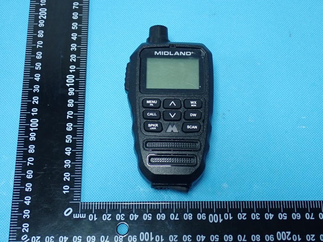
MMAMXMC95
Jun 10, 2026Wireless Bluetooth Microphone
Equipment Class
JAB - Part 15 Class B Digital Device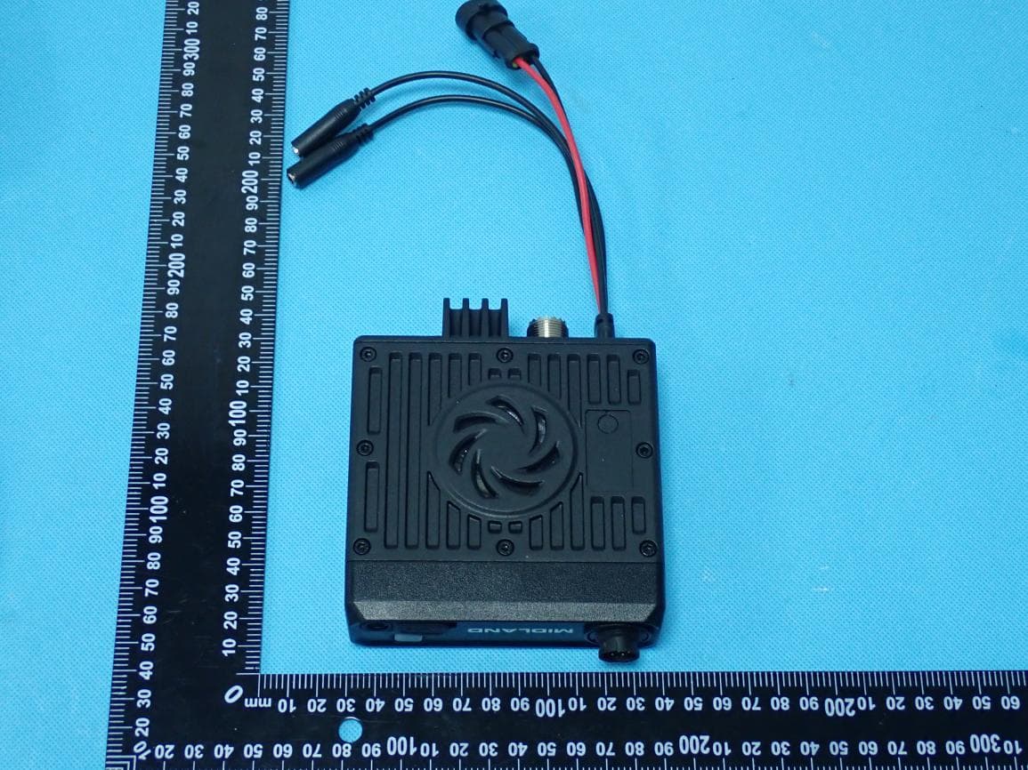
MMAMXT295
Jun 08, 2026GMRS Radio
Equipment Class
TNF - Licensed Non-Broadcast Transmitter Held to Face
MMACLIPTALK
Apr 27, 2026Transceiver
Equipment Class
DTS - Digital Transmission System
MMABR200S
Jan 13, 2026BUSINESS BAND TWO-WAY RADIO
Equipment Class
TNF - Licensed Non-Broadcast Transmitter Held to Face
MMAGXT67
Oct 29, 2023GMRS RADIO
Equipment Class
TNF - Licensed Non-Broadcast Transmitter Held to Face