MMA713200ABASE STATION
Midland Radio Corporation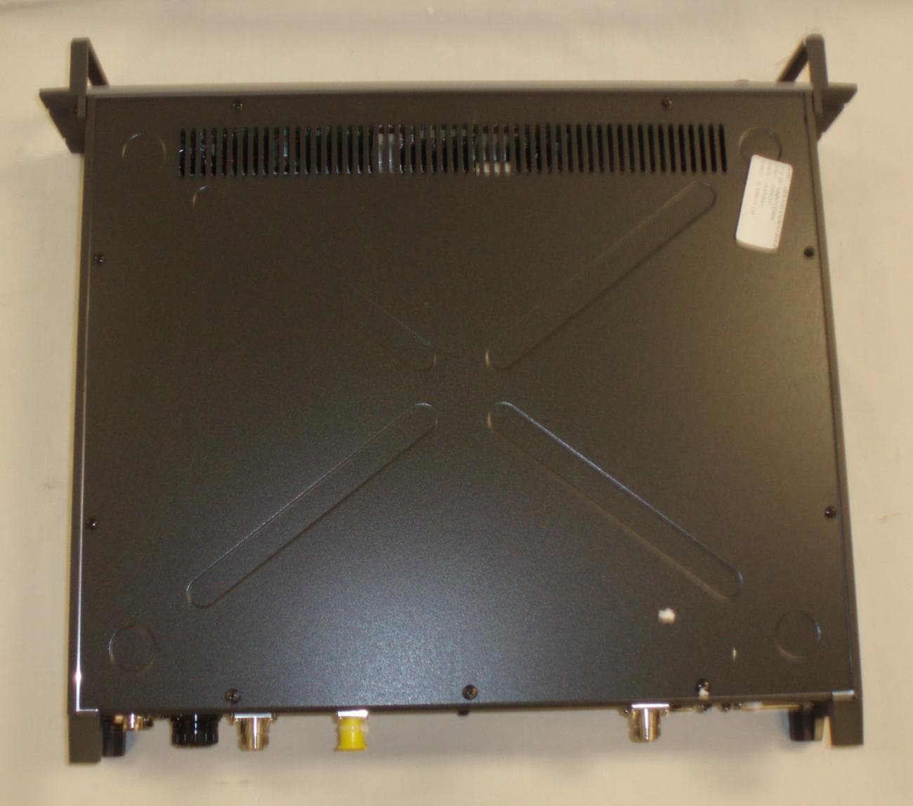
Click to zoom
Application Details
- Equipment Class
- TNB - Licensed Non-Broadcast Station Transmitter
- Date of Grant
- Feb 03, 2011
- Application Purpose
- Original Equipment
- Date of Application
- Feb 03, 2011
- Equipment Note
- BASE STATION
- Frequency Range
- 136.00000000 - 156.00000000
- Company
- Midland Radio Corporation
- Country
- United States
Documents & Files
Document Text
Text extracted from the exhibit documents filed with the FCC. Open a document above to read the original.
Users Manual
OPERATOR'S MANUAL BASE TECH II BASE/REPEATER STATION 05/09 Part Number 71-999000 Revision A Base Tech II Base/Repeater Station Operator’s Manual 2 © Midland Radio Corporation Introduction............................................................................................................................................ 3 Description............................................................................................................................................... 3 Features .................................................................................................................................................. 3 Controls, Indicators and Connectors ....................................................................................................... 4 Operation................................................................................................................................................ 8 Installation and Programming.................................................................................................................. 8 Basic Operation ....................................................................................................................................... 8 Front Panel Operation ........................................................................................................................... 10 Signaling................................................................................................................................................ 12 Scanning................................................................................................................................................ 15 Locking the Keypad ............................................................................................................................... 18 Changing Tone Signaling Systems........................................................................................................ 18 Displaying the Channel Information ...................................................................................................... 19 Display of Received Tone Frequencies. ................................................................................................ 20 Bar Graph Displays ............................................................................................................................... 21 LCD Display Back Light......................................................................................................................... 21 Transmit Power Change........................................................................................................................ 21 Calling Party ID Display......................................................................................................................... 22 Displaying any Radio's ID Number........................................................................................................ 22 Emergency Caller Display ..................................................................................................................... 23 Automatic Transmit in Repeater Mode .................................................................................................. 23 TX Test Mode ........................................................................................................................................ 24 Keypad Test Mode................................................................................................................................. 24 Frequency Band Test Mode .................................................................................................................. 25 Starting Message................................................................................................................................... 25 Serial Number Display........................................................................................................................... 26 EEROM Data Check Mode ................................................................................................................... 26 Hardware Error Detection...................................................................................................................... 27 RS232C Communications Error ............................................................................................................ 28 External Option Port/ Remote Control pin out............ .......................................... .................29 Base Tech II Base/Repeater Station Operator’s Manual 3 © Midland Radio Corporation INTRODUCTION Description The Base Tech II Base Repeater represents a technological advancement over previous models. The Base Tech II Base Repeater is comprised of separate modules all housed within one 2RU equipment cabinet. The receiver, transmitter, and PA unit are each enclosed within their own die-cast housing. Each one is then mounted directly on the large upper heatsink. A microprocessor-controlled interface module controls the channel selection, LCD Display, timers, interfaces, and signaling features. The RF power output is 25 — 50/ 60 watts or 50 — 100/ 110 watts on a continuous duty basis. The CTCSS module supports all EIA tones. All tones and different encode and decode tones can be set on a per channel basis during radio programming. Attention The antenna(s) used for this transmitter must be fixed-mounted on outdoor permanent structures with a separation distance of at least 6 meters from all persons during normal operation. The peak conducted output power at each antenna terminal must not exceed 250 Watts and the peak radiated output power must not exceed 1000 Watts EIPR. Users and installers must ensure that FCC requirements for satisfying RF exposure compliance are met. (See FCC Rules Part 1, Sections 1307 and 1310) Features o Simplex or two frequency Duplex operation o EEPROM programmable with a PC com…
Text truncated - open the document above for the full version.
ID Label/Location Info
Model: 71-3200A Serial #: _5304501__ FCC ID: _MMA713200A__ IC: _3690A-713200A _ MADE IN JAPAN
ID Label/Location Info
Rear View of 71-3200A/B FCC / IC Identification Label affixe d to rear panel in location shown. Model / FCC / IC Label here
Internal Photos
PA UNIT FRONT RX UNIT SERIAL PORT TX UNIT APPLICANT: MIDLAND RADIO CORP. FCC ID: MMA710100B INTERNAL PHOTOS
Parts List/Tune Up Info
Midland Radio 71-3200A/B VHF Base Tech II 7.0 ALIGNMENT PROCEDURES 7.1 RECEIVER UNIT 1. Pre-selector and Post-selector Filters Both the pre-selector and post-selector filters have been pre-tuned at the factory, so no alignment is required. 2. FVR001/FVR002 Alignment FVR001 adjusts the squelch tight level FVR002 is used to set the voltage at TP001 to 2.5 Volts DC 3. VCO Alignment The VCO is pre-aligned at the factory to cover the full A or B sub-band. However, if you need to re-adjust the VCO following a repair, set the VCO control voltage at TBD to 10.5 Volts DC by adjusting the coil winding spacing of L303 at the high end of the sub band. 7.2 TRANSMITTER UNIT 1) FVR201 Alignment This potentiometer adjusts the transmit modulation level. Carefully align this potentiometer to obtain as flat of deviation response as possible from the lowest to the highest frequency supported by the transmitter. 2) FVR202 Alignment This potentiometer determines low frequency (below 300Hz) deviation. When either or all of POCSAG, CTCSS and DCS are used, it is necessary to adjust this pot to provide enough deviations at low modulation frequencies. 3) FVR203 Alignment This potentiometer adjusts the maximum transmit deviation. 4) FVR204 Alignment This potentiometer sets the transmitter maximum output power level. 5) VCO Alignment The VCO is pre-aligned at the factory to cover the full A or B sub-band. However, if you need to re-adjust the VCO following a repair, set the VCO control voltage at TBD to 10.5 Volts DC by adjusting the coil winding spacing of L303 at the high end of the sub band. 7.3 POWER AMPLIFIER UNIT 1) FVR501 Alignment This potentiometer is used to adjust the minimum reverse power detection point when the transmit antenna port is terminated with 50 ohm load. 2) FVR502 Alignment This potentiometer is used to set the threshold point for reverse power detection. 3) FVR503 Alignment This potentiometer is used to set the threshold for transmit low power alarm detection. 4) FVR504 Alignment This potentiometer is used to set the maximum transmit power level of the Power Amplifier Unit. Do not exceed 120 Watts or the radio’s FCC type acceptance, whichever is lower. 7.4 LOGIC UNIT 1) VR401 Alignment This is the digital pulse code rotary switch on the Front Panel Unit used to set the volume. 2) VR402 Alignment This is the digital pulse code rotary switch on the Front Panel used to set the squelch level. 3) FVR401 Alignment This potentiometer, located on the Front Panel Unit and accessible from the front of the radio assembly, is used to fine-adjust the Hi-Power Level of the transmitter. 4) FVR402 Alignment This potentiometer, located on the Front Panel Unit and accessible from the front of the radio assembly, is used to fine-adjust the Lo-Power Level of the transmitter. 7.5 DESCRIPTION OF CIRCUITS TO STABILIZE OUTPUT FREQUENCY The transmitter uses a TCVXO (Temperature Compensated Voltage Controlled Crystal Oscillator) to generate 12.00MHz reference frequency for the transmitter PLL and VCO circuit. The accuracy of the TCVXO is less than +/- 0.00015% over the range of –30 degree C to +60 degree C. 7.6 DESCRIPTION OF CIRCUIT TO SUPPRESS SPURIOUS EMMISSIONS AND LIMIT MODULATIONS A multiple pole Low Pass Filter is used after the final power amplifier stage within the Power Amplifier Unit. It is designed to sharply attenuate spurious and harmonics frequencies above the highest frequency in the sub-band of the radio. Modulation limiting is performed by Tx audio processor AK2344 located on the Logic Unit. Internal limiting/compression amplifier provides excellent limiting with minimum distortion. In addition to modulation limiting, this device contains all circuitry to perform pre-emphasis, band pass shaping and CTCSS encoder.
Parts List/Tune Up Info
Midland Radio 71-3200A/B VHF Base Tech II 5.0 LIST OF SEMICONDUCTORS DESIGNATIONS AND FUNCTIONS 5.1 Tx VCO UNIT Q301 2SK508 Oscillator Q302 2SC4325 Amplifier Q303 2SC3583 VCO output amplifier Q304 DTA124EUA Switch Q305 2SC2351 B + filter Q306 DTYA114EUA B + switch IC301 uPC1688 Amplifier 5.2 Tx UNIT Q201 2SK3018 PTT buffer Q202 UMG1N Switch Q204 UMC2 Switch Q207 2SD2351 B + filter Q205 2SK3018 Charge pump Q208 RTU002P02 Charge pump Q209 2SK3018 Charge pump Q210 UMC2N Switch Q212 UMG1N Switch Q213 DTC124EUA Switch Q206 DTA124EUA Switch Q211 2SC3357 RF amplifier Q214 2SC4250 Switch Q215 2SC4325 Switch Q217 2SK3018 Switch IC201 BAJ0BCOFP 10v regulator IC202 XC6202P702P 7v regulator IC204 TC75W51F Mod LF amplifier IC205 TA75S01F Mod. Amplifier IC208 MB1511 PLL IC210 NJU7662M DC/DC converter IC209 TC4566F LPF, switch IC211 BA00CC0WFP Tx power adjust IC212-B NJM2904 Power control IC212-A NJM2904 Error amplifier IC203 XC6202P502M 5v regulator IC213 TA75S01F Mod. LF amplifier IC206 TC7TW125FU Level converter IC207 TC7TW125FU Level converter 5.3 PA UNIT Q501 2SK3018 Switch Q502 DTB143EK B + switch IC501-B BAM4558F Reverse power control IC501-A BAM4558F Error amplifier IC502 TA75S01F Power control IC504 AN78L05M 5v regulator IC503 TA75S01F Power signal amplifier PM510 RA08H1317M Driver amplifier Q504 RD70HVF1 Power amplifier Q505 RD70HVF1 Power amplifier 5.4 RX VCO UNIT Q301 2SK508 Oscillator Q302 2SC4325 Amplifier Q303 2SC3583 VCO output amplifier Q304 DTA124EUK Switch Q305 2SC2351 B + filter Q306 DTYA114EUA B + switch IC301 uPC1688 Amplifier 5.5 RX UNIT Q861 3SK177 RF amplifier Q810 2SK508 1 st High IF amplifier Q809 2SD2351 B + filter Q806 RTU002P02 Charge pump Q805 2SK3018 Charge pump Q807 2SK3018 Charge pump Q808 UMC2N Switch Q804 UMC2N Switch Q811 DTA144EUA Switch Q803 33061MCH Rx switch Q802 2SD2351 Rx switch Q801 2SK3018 Rx switch Q812 2SC4250 Switch Q813 2SC4325 Switch Q814 2SC4325 Switch IC806 MB1511 PLL IC807 NJU7662M DC/DC inverter IC808 TC4566F LPF switch IC805 XC6202P502M 5v regulator IC809 TA75S01F VCO error amplifier IC811 SPM5001 1 st mixer IC802 XC221A200 AF LPF IC801 BA70BCOFP 7v regulator IC803 TCWT125FU Level converter IC804 TCWT125FU Level converter IC810 XC221A1200 DC amplifier IC812 XC6201P502M 5v regulator 5.6 IF UNIT Q001 2SC4250 1st IF amplifier Q002 2SK880 Wide/Narrow switch Q003 DTC323TU Wide/Narrow switch Q004 2SK880 Wide/Narrow switch Q005 2SK3018 Wide/Narrow switch Q006 2SD2351 Noise amplifier Q007 XP01501 Squelch switch IC001 TA31136FNG 2nd IF/oscillator/detector IC002 TC75W51FU AF amplifier Logic Unit and Front Panel Unit semiconductor parts are the same as the MMA710100B radio.
Parts List/Tune Up Info
71-3200A/B Parts List Parts listed for B-sub band. See schematics for A sub-band substitutions. KEYPAD UNIT MISCELLANEOUS 00-6200-510-130-000+ CN405 SKHMQLE010 SWITCH for CH,SCAN,MUTE,SHIFT,1,2,3,4, 5,6,7,8,9,0,A,B,C,D,#,* 51KEY87-1 KEYPAD UNIT PCB 4A10-2996 STANDOFF SE-3 X 10 SEMS SCREW MISCELLANEOUS 00-6200-508-130-000+ CN407 SLA-370MT-3F D415 SPPH23056A SW401 RY-6459 VR401 RY-6460 VR402 51VRS87-2 VOLUME / SQUELCH PCB 4A10-2988 BUTTON SE-3 X 10 SEMS SCREW MISCELLANEOUS 2A10-0213 FRONT PANEL 4A10-2985 BUTTON 4A10-2987 WINDOW 4A10-2989 KNOB 4A10-3001 SPEAKER GRILL 4A10-3026 SPEAKER SPACER 4A10-3047 TAPE FOR WINDOW 4A-S499 CONNECTOR CABLE KS-110 SPEAKER PN-3 X 8 TP SCREW TM12832ABCW-6 LCD401 S-G8022#01J401 4A-S429FLC402 4A-S471FLC403 4A-S585FLC405 4A-S584FLC407 BP53RD030310120MCN402-CN1 4A10-3004BSPACER 4A10-3045COLLAR 4A10-3079PLATE 51FR087-4PCB SE-3 X 10SEMS SCREW FRONT PANEL UNIT VOLUME / SQUELCH UNIT INTERGRATED CIRCUITS TA75S558F(TE85R) IC401 TC74HC373AF(TP1,F) IC402 TA78M05F(TE16L,Q) IC403 TD1519C IC404 PQ12RH11 IC405 NJU7662M-T1 IC406 BU4S01F-TR IC407 TRANSISTORS DTC114EKA-T146 Q401 FMG9A-T148 Q402,Q403 2SD1766-T100 Q404 2SD2351-T106 Q405 2SJ634-TL Q406 UMC2N-TR Q407 2SA1434-TB Q408,Q409,Q410 DIODES MU16-4101 D401 MU16-3101 D402 MU16-2101 D403 MU16-5101 D404 1SS355-TE17 D405,D406,D407,D408,D409,D4 14 DA204U-T106 D411,D412 CAPACITORS GRM216B11H102KA01D C401,C421,C410 GRM216B11E104KA01D C431 GRM2162C1H101JA01D C404 GRM2162C1H271JA01D C407,C408 GRM31MB11H104KA01D C406,C411 GRM31MB11C105KA01L C402,C422 TEESVA1V105M8R C417 KMG16VB-220 C428 KMG16VB1000M C420 KMG35VB470M C418,C419 EMVK160ADA100MD55G C405,C409,C412,C413,C414 EMVK350ADA4R7MD55G C425 EMVK500ADA1R0MD55G C403 EMVK160ADA470MF55G C424 RESISTORS MCR10EZHJ000 R401,R451 MCR10EZHJ102 R406 MCR10EZHJ103 R407,R439,R442,R449,R455,R4 58 MCR10EZHJ104 R409,R410,R456,R457 MCR10EZHJ152 R453 MCR10EZHJ153 R405 MCR10EZHJ181 R427 MCR10EZHJ183 R420 MCR10EZHJ221 R417 MCR10EZHJ222 R412,R414,R445 MCR10EZHJ223 R424 MCR10EZHJ224 R454 MCR10EZHJ273 R408 MCR10EZHJ330 R418 MCR10EZHJ333 R448 MCR10EZHJ470 R422,R423,R428,R429 MCR10EZHJ471 R440 MCR10EZHJ472 R425,R426,R430,R431,R432,R4 33,R434,R435,R436,R437,R438, R441 MCR10EZHJ473 R411,R419,R459 MCR10EZHJ560 R415,R416 MCR10EZHJ562 R450 MCR10EZHJ563 R446 MCR10EZHJ822 R421,R452 MCR18EZHJ100 R447 MCR18EZHJ4R7 R444 POTENTIOMETERS GF06P 10KFVR401 GF06P 100KFVR402 G32AT 103FVR403 THERMISTORS TN10-4C103KTTH401 CONNECTORS 290A-88-30-119CN401 00-6200-520-330-000+CN402 00-6200-516-230-000+CN403 00-6200-510-130-000+CN404 00-6200-508-130-000+CN406 B 3P-VHCN408 SB20-02WSCN409 FF20-TAMEP1CP401 LOGIC UNIT INTERGRATED CIRCUITS AK2344IC2,IC3 HN58C65FP-25IC7 NJM2405M-T1IC6 NJM2073MIC16 AN78L05MIC4,IC5 UPD78F0058GCIC1 RN5VL22AA-TLIC9 BU4S01-TRIC12 BU4S66-TRIC17 BU4S81-TRIC11,IC15 TS272CDIC13,IC14 TA75S01F(TE85R,F)IC10 TC74HC373AF(TP1,F)IC8 TC7W74FUIC18 TRANSISTORS DTC124EKA-T146Q7 2SK209-Y(TE85R)Q1,Q2,Q3,Q4 RN6001(TE12R,C)Q6 DIODES 1SS355-TE17 D1,D2,D3,D4,D5,D8, D13,D14,D15 DAP202U-T106D9,D10 DAN202U-T106D12 RB501V-40TE-17D7,D11 CRYSTALS DS-MAT309(4.19MHZ)X1 3.6864MHZ(SMD)X2,X3 INDUCTOR FERRITES FBMH3216HM501NTBL1 BLM21B421SPT BL2,BL3,BL4,BL5,BL6, BL7 CAPACITORS GRM216B11H102KA01D C80,C81,C82,C83,C84,C85 GRM216B11H103KA01D C11,C36,C47,C48,C49,C52,C75 GRM216B11E104KA01D C5,C6,C19,C21,C23,C27,C28,C3 2,C33,C60,C61,C64,C68,C70,C7 3,C76,C79 GRM216B11H123KA01D C15 GRM216B11H152KA01D C7 GRM216B11E333KA01D C50 GRM21BB11H473KA01L C20,C37,C42,C44,C62,C63,C66 GRM216B11H682KA01D C65 GRM2162C1H220JZ01D C38,C39,C45,C46 GRM2162C1H221JA01D C13 GRM2162C1H330JA01D C43 GRM2162C1H331JA01D C8,C14 GRM2162C1H470JZ01D C22,C55,C67 GRM2162C1H820JZ01D C31,C51 GRM31MB11C105KA01L C58,C69 GRM31MB11C225KA35L C12,C24 TEESVA1V105M8R C2,C3,C16,C17,C25,C53,C54 TEESVA1E474M8R C40,C72 TEESVA1V224M8R C10,C59 TEESVB21C106M8R C74, EMVK160ADA470MF55G C4,C71,C77,C78 EMVK350ADA4R7MD55G C1 EECS5R5H474 C9 VARIABLE CAPACITORS TZV02R200A110FVC1 RESISTORS MCR03EZHJ225R100 MCR10EZHJ101 R13 MCR10EZHJ102 R40,R98 MCR10EZHJ103 R14,R17,R32,R44,R49,R54,R61, R63,R82,R86,R99 MCR10EZHJ104 R0,R7,R9,R21,R23,R37,R58,R65 ,R66,R71,R79,R83,R91 MCR10EZHJ105 R5,R38,R50 MCR10EZHJ113 R2 MCR10EZHJ124 R64,R68 MCR10EZHJ153 R16 MCR10EZHJ154 R1,R20,R24,R29,R30,R34,R59,R 60,R70,R72,R90,R95 MCR10EZHJ183 R25 MCR10EZHJ184 R4,R73 MCR10EZHJ222 R27 MCR10EZHJ223 R19,R35,R36,R47,R69 MCR10EZHJ224 R55 MCR10EZHJ225 R03,R3 MCR10EZHJ271 R87,R88 MCR10EZHJ273 R4,R6,R8,R94 MCR10EZHJ333 R53,R56 MCR10EZHJ393 R15 MCR10EZHJ394 R97 MCR10EZHJ3R3 R74 MCR10EZHJ472 R22,R39,R41,R76,R78,R85,R96 MCR10EZHJ473 R5,R10,R18,R26,R33,R42,R67,R 80,R84,R89 MCR10EZHJ474 R75 MCR10EZHJ562 R2,R11 MCR10EZHJ563 R43 MCR10EZHJ682 R12 MCR10EZHJ683 R57 MCR10EZHJ823 R01,R28,R52,R62 MCR10EZHJ000 R45,R46 MCR50EZHJ4R7 R77 POTENTIOMETERS G32AT 203FVR1 G32AT 204FVR2 G32AT 503FVR3 G32AT 103FVR4 RESISTOR ARRAYS MNR14E0ABJ472 RA1,RA2,RA3 TEST POINTS RCTTP1 CONNECTORS SB20-03WSCN6 DIC-149-3PJP1,JP2 DIC-128JS 00-6200-520-330-000+CN1,CN9 00-6200-516-230-000+CN2,CN3,CN7,CN8 08-6212-008-340-800+CN4,CN5 MISCELLANEOUS 51LOG87-5PCB INTERGRATED CIRCUITS BA4116FVIC001 M62551GP-C60QIC002 TRANSISTORS 2SC4250(TE85R,F)Q001 2SK880GR(TE85L,F)Q002, Q004 DTC623TU-T106Q003 2SK3018-T106Q005 2SD2351-T106Q006 XP01501Q007 DIODES 1SS295(TE85L,F)D001 1SS356-TW11D002 1SS400-TE61D003 02DZ3.9-X(TPH3,F)D004 CRYSTALS 48.955MHZX001 MF48QXF001, XF002 COILS ELJ-FCR82KFL001 HK2125R22JL002 KQ1008TTER47KL007 RX IF UNIT CAPACITORS GRM188B11H102KA01DC004, C006, C007, C010, C035, C034 GRM188B11H103KA01DC008, C027 GRM188B11E104KA01DC016 GRM188B11H153KA01DC014, C024, C040 GRM188B11H223KA01DC019, C029 GRM188B11H332KA01DC012, C021 GRM188B11H471KD01DC037, C039 GRM188B11C473KA01DC020 GRM1882C1H100JA01DC038 GRM1882C1H150JA01DC005 GRM1882C1H110JA01DC041 GRM1882C1H330JA01DC011 GRM1882C1H470JA01DC013 GRM1882C1H560JA01DC028 GRM1882C1H561JA01DC022, C023 GRM1882C1H680JA01DC017 MCH185A070CKC002 MCH185A080CKC001, C003 GRM216B11H102KD01DC009 GRM216B11C105KA01LC015, C026 GRM21BB10J225KA01LC018 GRM40EZHJ242C030…
Text truncated - open the document above for the full version.
RF Exposure Info
2/4/2011 Page 1 of 3 FCC RF Exposure Requirements General information: Device category: Fixed per Part 2.1091 Environment: Uncontrolled Exposure Fixed mounted devices that operate under Part 90 of this chapter are subject to routine environmental evaluation for RF exposure prior to equipment authorization or use if they operate at frequencies of 1.5 GHz or below and their effective radiated power (ERP) is 1.5 watts or more. However, compliance with the power density limits of 1.1310 is not required. Antenna: The manufacturer does not specify an antenna. A typical fixed mounted antenna has a gain of 3 dBi. This device has provisions for operation in a fixed location. Configuration Antenna p/n Type Max. Gain (dBi) Fixed mounted Any omni 3 Operating configuration and exposure conditions: The conducted output power is 110 Watts. Typical use qualifies for a maximum duty cycle factor of 50%. The manufacturer also markets this device only for occupation use. - Part 2.1091 states that devices are excluded from routine evaluation if the EIRP is less than 2.46Watt (or 1.5WERP). - Fixed operation: A typical installation consists of an antenna system with a coaxial cable of the type RG 8U which has a loss of 1dB for a length of 40 feet at VHF frequencies. MPE Calculation: The minimum separation distance is calculated as follows: The limit for general population/uncontrolled exposure environment below 300 MHz is 0.2 mW/cm 2 . 2/4/2011 Page 2 of 3 Frequency: 136-156 MHz The conducted power output is 110 watt. The coax loss was taken as 1 dB. Antenna gain was taken as 3 dBi 50% talk time in 30 minutes 2/4/2011 Page 3 of 3 Conclusion: The MPE calculations show that based on the conditions presented a safe separation distance of 73 inches (6 ft) between the antenna, including any radiating structure, and any persons when normally operated complies with the FCC limits for RF exposure. Proposed RF exposure safety information to include in User’s Manual: “FCC RF Exposure Requirements: See user’s manual.
RF Exposure Info
1/31/2011 Page 1 of 3 FCC RF Exposure Requirements General information : Device category: Fixed per Part 2.1091 Environment: Uncontrolled Exposure Fixed mounted devices that operate under Part 90 of this chapter are subject to routine environmental evaluation for RF exposure prior to equipment authorization or use if they operate at frequencies of 1.5 GHz or below and their effective radiated power (ERP) is 1.5 watts or more. However, compliance with the power density limits of 1.1310 is not required. Antenna: The manufacturer does not specify an antenna. A typical fixed mounted antenna has a gain of 3 dBi. This device has provisions for operation in a fixed location. Configuration Antenna p/n Type Max. Gain (dBi) Fixed mounted Any omni 3 Operating configuration and exposure conditions: The conducted output power is 110 Watts. Typical use qualifies for a maximum duty cycle factor of 50%. The manufacturer also markets this device only for occupation use. - Part 2.1091 states that devices are excluded from routine evaluation if the EIRP is less than 2.46Watt (or 1.5WERP). - Fixed operation: A typical installation consists of an antenna system with a coaxial cable of the type RG 8U which has a loss of 1dB for a length of 40 feet at VHF frequencies. MPE Calculation: The minimum separation distance is calculated as follows: The limit for general population/uncontrolled exposure environment below 300 MHz is 0.2 mW/cm 2 . 1/31/2011 Page 2 of 3 Frequency: 138-156 MHz The conducted power output is 110 watt. The coax loss was taken as 1 dB. Antenna gain was taken as 3 dBi 50% talk time in 30 minutes 1/31/2011 Page 3 of 3 Conclusion: The MPE calculations show that based on the conditions presented a safe separation distance of 73 inches (6 ft) between the antenna, including any radiating structure, and any persons when normally operated complies with the FCC limits for RF exposure. Proposed RF exposure safety information to include in User’s Manual : “FCC RF Exposure Requirements: See user’s manual.
Test Report
FCC PART 90 AND IC RSS-119, RSS-GEN TEST REPORT APPLICANT MIDLAND RADIO CORPORATION 5900 PARRETTA DRIVE KANSAS CITY MISSOURI 64120 USA FCC ID MMA713200A IC CERTIFICATION 3690A713200A MODEL NUMBER 71-3200A PRODUCT DESCRIPTION BASE STATION DATE SAMPLE RECEIVED 1/17/2011 DATE TESTED 1/20/2011 TESTED BY Nam Nguyen APPROVED BY Mario de Aranzeta TIMCO REPORT NO. M\MidlandRadio MMA\109AT11\109AT11TestReport.doc TEST RESULTS PASS FAIL THE ATTACHED REPORT SHALL NOT BE REPRODUCED EXCEPT IN FULL WITHOUT THE WRITTEN APPROVAL OF TIMCO ENGINEERING, INC. TABLE OF CONTENTS 849 NW STATE ROAD 45 NEWBERRY, FL 32669 USA PH: 888.472.2424 OR 352.472.5500 FAX: 352.472.2030 EMAIL: [email protected] HTTP: //WWW.TIMCOENGR.COM Certificate # 0955-01 Applicant: MIDLAND RADIO CORPORATION FCC ID: MMA713200A IC CERT #: 3690A713200A Report: M\MidlandRadio MMA\109AT11\109AT11TestReport.doc Page 2 of 23 TABLE OF CONTENTS GENERAL REMARKS ......................................................................................................... 3 GENERAL INFORMATION .................................................................................................. 4 TEST PROCEDURES ......................................................................................................... 5 RF POWER OUTPUT .......................................................................................................... 6 MODULATION CHARACTERISTICS .................................................................................... 7 AUDIO FREQUENCY RESPONSE ....................................................................................... 8 AUDIO LOW PASS FILTER ................................................................................................. 9 AUDIO INPUT VERSUS MODULATION ............................................................................. 10 OCCUPIED BANDWIDTH ................................................................................................. 11 SPURIOUS EMISSIONS AT ANTENNA TERMINALS (CONDUCTED) ................................... 14 FIELD STRENGTH OF SPURIOUS EMISSIONS ................................................................. 17 FREQUENCY STABILITY .................................................................................................. 19 TRANSIENT FREQUENCY BEHAVIOR .............................................................................. 20 EMC EQUIPMENT LIST ................................................................................................... 23 Applicant: MIDLAND RADIO CORPORATION FCC ID: MMA713200A IC CERT #: 3690A713200A Report: M\MidlandRadio MMA\109AT11\109AT11TestReport.doc Page 3 of 23 GENERAL REMARKS The attached report shall not be reproduced except in full without the written permission of Timco Engineering Inc. The test results relate only to the items tested. Summary The device under test does: fulfill the general approval requirements as identified in this test report not fulfill the general approval requirements as identified in this test report Attestations This equipment has been tested in accordance with the standards identified in this test report. To the best of my knowledge and belief, these tests were performed using the measurement procedures described in this report. All instrumentation and accessories used to test products for compliance to the indicated standards are calibrated regularly in accordance with ISO 17025: 2005 requirements. Testing Certificate # 0955-01 I attest that the necessary measurements were made, under my supervision, at: Timco Engineering Inc. 849 NW State Road 45 Newberry, Fl 32669 Authorized Signatory Name: Mario de Aranzeta C.E.T. Compliance Engineer/ Lab. Supervisor Date: February 2, 2011 Applicant: MIDLAND RADIO CORPORATION FCC ID: MMA713200A IC CERT #: 3690A713200A Report: M\MidlandRadio MMA\109AT11\109AT11TestReport.doc Page 4 of 23 GENERAL INFORMATION DUT Specification DUT Description BASE STATION FCC ID MMA713200A IC Certification 3690A713200A Model Number 71-3200A Serial Number N/A Operating Frequency 136.00 – 156.00 MHz Test Frequencies (138.0, 148.0, and 156.0) MHz Channel Capacity 99 Type of Emission 11K2F3E Modulation FM DUT Power Source 110–120Vac/50– 60Hz DC Power 13.8V Battery Operated Exclusively Test Item Prototype Pre-Production Production Type of Equipment Fixed Mobile Portable Test Conditions The temperature was 26ºC with a relative humidity of 50%. Modification to the DUT None Test Exercise The DUT was placed in continuous transmit mode. Applicable Standards ANSI/TIA 603-C:2004, FCC CFR 47 Part 90 Test Facility Timco Engineering Inc. at 849 NW State Road 45 Newberry, FL 32669 USA. Applicant: MIDLAND RADIO CORPORATION FCC ID: MMA713200A IC CERT #: 3690A713200A Report: M\MidlandRadio MMA\109AT11\109AT11TestReport.doc Page 5 of 23 TEST PROCEDURES Power Line Conducted Interference: The procedure used was ANSI/TIA 603-C:2004 using a 50uH LISN. Both lines were observed with the DUT transmitting. The bandwidth of the spectrum analyzer was 10 kHz with an appropriate sweep speed. Bandwidth 20 dB: The measurements were made with the spectrum analyzer's resolution bandwidth (RBW) = 1 MHz and the video bandwidth (VBW) = 3 MHz and the span set as shown on plot. Power Output: The RF power output was measured at the antenna feed point using a peak power meter. Antenna Conducted Emissions: The RBW = 100 kHz, VBW = 300 kHz and the span set to 10.0 MHz and the spectrum was scanned from 30 MHz to the 10 th harmonic of the fundamental. Above 1 GHz the resolution bandwidth was 1 MHz and the VBW = 3 MHz and the span to 50 MHz. Radiation Interference: The test procedure used was ANSI/TIA 603-C: 2004 using an Agilent spectrum receiver with pre-selector. The bandwidth (RBW) of the spectrum receiver was 100 kHz up to 1 GHz and 1 MHz above 1 GHz with an appropriate sweep speed. The VBW above 1 GHz was 3 MHz. The analyzer was calibrated in dB above a micro volt at the output of the antenna. Applicant: MIDLAND…
Text truncated - open the document above for the full version.
Contact Information
Applicant
Butch Rittmann(Director of Operations)
Test Firm
Timco Engineering, Inc.Bruno Clavier
Technical Specifications
| # | Rule Parts | Frequency Range | Power Output | Emission | Tolerance |
|---|---|---|---|---|---|
| 2 | 9 | 136 MHz - 156 MHz | 5 W | 11K2F3E | 1.5 ppm |
Other Applications from Midland Radio Corporation
MMAMXMC95
Jun 10, 2026Wireless Bluetooth Microphone
Equipment Class
JAB - Part 15 Class B Digital Device
MMAMXT295
Jun 08, 2026GMRS Radio
Equipment Class
TNF - Licensed Non-Broadcast Transmitter Held to Face
MMACLIPTALK
Apr 27, 2026Transceiver
Equipment Class
DTS - Digital Transmission System
MMABR200S
Jan 13, 2026BUSINESS BAND TWO-WAY RADIO
Equipment Class
TNF - Licensed Non-Broadcast Transmitter Held to Face
MMAGXT67
Oct 29, 2023GMRS RADIO
Equipment Class
TNF - Licensed Non-Broadcast Transmitter Held to Face