MMA75785CB Transceiver
Midland Radio Corporation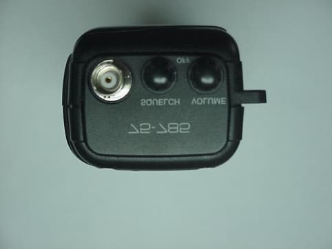
Click to zoom
Application Details
- Equipment Class
- TNF - Licensed Non-Broadcast Transmitter Held to Face
- Date of Grant
- Jul 13, 2000
- Application Purpose
- Original Equipment
- Date of Application
- Apr 18, 2000
- Equipment Note
- CB Transceiver
- Frequency Range
- 26.96500000 - 27.40500000
- Company
- Midland Radio Corporation
- Country
- United States
Documents & Files
Document Text
Text extracted from the exhibit documents filed with the FCC. Open a document above to read the original.
External Photos
Front View Back View Left Side View Right Side View Top View
Internal Photos
PCB Top View PCB, Bottom View
Parts List/Tune Up Info
8. ALIGNMENT INSTRUCTIONS Warning : Any repairs or adjustment should be made under the supervision of a qualified radio-telephone technician. 8.1. VCO a. Connect the power supply (DC 13.8 V) b. Connect the oscilloscope probe to test point c. Adjust the coil L601 for 2V at 1-Ch RX. d. Check that T401 voltmeter of receiver reads from 2 to 4 volts. 8.2. Transmitter a. TX Power alignments With RF voltmeter at base of Q701, transmit of channel 19. Adjust in turn L701,L702 for maximum reading on RF voltmeter. Repeat as needed. Remove RF voltmeter. b. Max Mod Alignments Adjust RV401 to obtain 90% MOD. At 16 dB greater than 50% MOD. AF 1 KHz. c. Final Check 1. Output power should be from 3.6 to 4.0 watts. 2. Frequency should be within +400 Hz of channel center frequency. 3. Spurious content as observed on spectrum synthesizer should be at least 60 dB below carrier. 4. With 2500 Hz modulation at 16 dB greater than that required to produce 50% modulation, occupied bandwidth should be at least 2 dB better than limit spec.
Parts List/Tune Up Info
CB Transceiver PLL Frequency Synthesizer and Controller Overview This 27 MHz band, PLL frequency synthesizer LSI chip is designed specifically for CB transceivers. The specifications are suited for use in U.S.A.(FCC). Functions The LC7185-8750 incorporates PLL circuitry and a controller for CB applications on a single CMOS chip. The controller handles the PLL circuitry, frequency data ROM, channel preset/recall RAM, and LED display driver. It also supports channel scan, channel preset/recall, and emergency channel call. Features 1. A built-in programmable divider for the 16 MHz VCO 2. Transmission is inhibited when the PLL is unlocked (digital lock monitor). 3. Direct channel 9 or 19 selection (sliding switch) 4. A 7-segment, 2-character LED display 5. ‘‘PA’’ is displayed in public announcement mode. 6. Output beep-tone control circuitry 7. Up to 5 channel settings can be stored in memory. 8. 4×3 key matrix implementation Package Dimensions unit : mm 3061-DIP30S [LC7185-8750] SANYO : DIP30S (400 mil) Specifications Absolute Maximum Ratingsat Ta = 25°C, V SS =0V ParameterSymbolConditionsRatingsUnit Maximum supply voltageV DD maxPin V DD –0.3 to +9.0V Input voltageV IN 1 maxPins HOLD, TX–0.3 to +15V V IN 2 maxInput pins other than V IN 1 max–0.3 to V DD +0.3V Output voltageV O 1 maxPins SA, SB, SC, SD, SE, SF, SG, D1, D2–0.3 to +15V V O 2 maxPins UL, BEEP–0.3 to +15V V O 3 maxPin PD–0.3 to V DD +0.3V V O 4 maxOutput pins other than mentioned above –0.3 to V DD +0.3V Output CurrentI O 1 maxPins SA, SB, SC, SD, SE, SF, SG0 to +30mA I O 2 maxPins D1, D20 to +10mA I O 3 maxPins UL0 to +20mA I O 4 maxPin BEEP0 to +10mA Allowable power dissipation Pd max(Ta%85°C)350mW Operating temperatureTopr–40 to +85°C Storage temperatureTstg–55 to +125°C Ordering number: EN 3356A CMOS IC LC7185-8750 SANYO Electric Co.,Ltd. Semiconductor Bussiness Headquarters TOKYO OFFICE Tokyo Bldg., 1-10, 1 Chome, Ueno, Taito-ku, TOKYO, 110-8534 JAPAN 73098HA(II)/5220TA No.3356-1/12 Allowable Operating Conditionsat Ta = –40 to +85°C, V SS =0V ParameterSymbolConditionsmintypmaxUnit Supply voltageV DD 5.08.0V Input high-level voltage V IH 1 Pins HOLD, TX0.7V DD 12V V IH 2 Pin INIT3.2V DD V V IH 3 Pins KI1, KI2, KI3, KI40.6V DD V DD V Input low-level voltage V IL 1 Pins HOLD, TX00.3V DD V V IL 2 Pin INIT01.3V V IL 3 Pins KI1, KI2, KI3, KI400.4V DD V Output voltage V OUT 1 Pins SA, SB, SC, SD, SE, SF, SG, D1, D2013V V OUT 2 Pins UL, BEEP08V Input frequency f IN 1 Pin XIN (sine wave, capacitor coupled)1.0 10.2415 MHz f IN 2 Pin PIN (sine wave, capacitor coupled)1030 MHz Input amplitude V IN 1 Pin XIN (sine wave, capacitor coupled)0.51.5 Vrms V IN 2 Pin PIN (sine wave, capacitor coupled)0.151.5 Vrms Required oscillating frequency X’tal Pins XIN, XOUT (CI%50Ω)5.0 10.2415 MHz Electrical Characteristicsat under allowable operating conditions ParameterSymbolConditionsmintypmaxUnit Internal feedback resistance Rf1 Pin XIN1.0MΩ Rf2 Pin PIN500kΩ Pull-down resistorRpdN Pins KI1, KI2, KI3, KI4, TEST305070kΩ Input high-level current I IH 1 Pins HOLD, TX V I =12V5.0μA I IH 2 Pin INIT V I =V DD 5.0μA I IH 3 Pin XIN V I =V DD 25μA I IH 4 Pin PIN V I =V DD 50μA Input low-level current I IL 1 Pins HOLD, TX V I =V SS 5.0μA I IL 2 Pin INIT V I =V SS 5.0μA I IL 3 Pin XIN V I =V SS 25μA I IL 4 Pin PIN V I =V SS 50μA Output high-level voltage V OH 1 Pins KO1, KO2, KO3 I O =1mAV DD –2.0 V DD –1.0 V DD –0.5V V OH 2 Pin PD I O = 0.5 mAV DD –1.0V Output low-level voltage V OL 1 Pins KO1, KO2, KO3 I O = 20 μA0.61.01.4V V OL 2 Pin PD I O = 0.5 mA1.0V V OL 3 Pin BEEP I O = 2 mA1.0V V OL 4 Pins SA, SB, SC, SD, SE, SF, SG I O =20mA 1.0V V OL 5 Pins D1, D2 I O = 5 mA1.0V V OL 6 Pin UL I O =10mA1.0V Output leakage current I OFF 1 Pins SA, SB, SC, SD, SE, SF, SG, D1, D2 V O =13V 5.0μA I OFF 2 Pins UL, BEEP V O =8V5.0μA High-level tristate leakage current I OFFH Pin PD V O =V DD 0.0110.0nA Low-level tristate leakage current I OFFL Pin PD V O =V SS 0.0110.0nA Supply current I DD 1 Normal mode *1 (PLL operates) 510mA I DD 2 Hold mode V DD = 3.2 V *2 (memory backup) V DD = 8.0 V 5 15 μA μA *1: f IN 2 = 20 MHz (PIN) V IN 2 = 0.15 Vrms X’tal = 10.240 MHz TX = HOLD = INIT = V DD Other inputs = V SS Other outputs = open *2: HOLD = V SS TX = INIT = V DD Other inputs = V SS Other outputs = open Note: Be careful that the dielectric strength of pins SA, SB, SC, SD, SE, SF, D1, D2, UL, BEEP are weak. LC7185-8750 No. 3356-2/12 Pin Assignment Block Diagram LC7185-8750 No. 3356-3/12 Pin Descriptions TXTransmit/receive selectPDCharge pump output HOLD Hold mode selectNCNC pin INIT Initial inputSA to SGSegment driver (for display) TESTTest point (input)D1, D2Digit output (for display) V DD ,V SS 1, V SS 2Power supplyKI1 to KI4Key inputs PINProgrammable divider inputKO1 to KO3Key scan outputs XIN, XOUTCrystal oscillator input, output (10.240 MHz) BEEPBeep-tone control output UL Unlock detection signal output Key Matrix CH9Emergency CH9 recallMEStation Memory Enable CH19Emergency CH19 recallM1 to M5Station Memory recall PAPublic announcement displayUP/DN/ME/M1 to 5 Momentary SW MODE 1/2Display ModeCH9/CH19/PASlide SW UPCH up/scanMODE 1/2Diode DNCH down/scan LED Display Configuration (Common anode/7 segment) LC7185-8750 No. 3356-4/12 Pin Description Pin NamePin No.TypeDescription TX 30 . Transmit/receive select TX = ‘‘0’’...Transmit, TX = ‘‘1’’...Receive HOLD26 . Hold mode select HOLD = ‘‘0’’...Hold mode select = ‘‘1’’...Normal mode select INIT 25 . Reset line INIT = ‘‘0’’...Reset TEST22 . Test point (input) Tie to ground or leave floating V DD 24 . Power supply (+) Normal mode: 5.0 to 8.0 V Hold mode:^3.2 V V SS 221 . Channel display LED driver ground PIN23 . Programmable divider input 150 mVrms min Hold mode: Programmable divider is disabled. XIN XOUT 20 19 . Crystal oscillator Frequency: 10.24 MHz Hold mode: Oscillator is disabled. PD27 . Charge pump output from the phase comparator. If the frequency of fV (the signal obtained by dividing the PIN input by N) is higher than that …
Text truncated - open the document above for the full version.
RF Exposure Info
To: Tom Bishop, null From: Joe Dichoso [email protected] FCC Application Processing Branch Re: FCC ID MMA75785 Applicant: Midland Consumer Radio Correspondence Reference Number: 14230 731 Confirmation Number: EA97405 Date of Original E-Mail: 05/25/2000 Please place your reply in the RF exposure info folder. Midland Consumer Radio, EA 97405 - 1. Although hand-held, push-to-talk device are categorically excluded from routine RF exposure evaluation for demonstrating SAR compliance, they are not exempted from compliance. Because of the relatively higher output available for this device, additional information is needed to determine if SAR compliance can be assured or if a request for RF exposure evaluation under the provisions of 1.1307(d) would be necessary. Please provide the following information, if applicable, for determining if a request for SAR evaluation is necessary - (a) the type and number of antenna(s) to be used for this device and relevant information, such operating instructions and certain caution statements, provided to users for ensuring SAR compliance No more than two types of rubber covered helically wound antenna (b) maximum antenna gain and physical length of antenna(s) indicated in (a) The maximum expected gain is -20dBd from an antenna no more than 11 inches long (c) can this device sustain continuous operation with respect to its hardware capabilities and allowable operating functions ? The transmitter can maintain only a 20% duty cycle without overheating, causing damage to circuit elements. (d) are there any other hardware or operating restrictions that could limit a person's RF exposure ? No. (e) is source-based time-averaging (see 2.1093 of rules) applicable to reduce the average output power ? No. (f) this device has headset and belt-clip accessories that would allow body-worn operations, what is the minimum separation distance between any part of the antenna(s) and the user's body in this operating configuration ? One i nc h. (g) can specific operating instructions be given to users to eliminate any potential RF exposure concerns for both front-of-the-face and body-worn operating configurations ? Yes (h) any other applicable information the applicant may provide that can serve as effective means for ensuring RF exposure compliance. The maximum power output drops to 3 Watts on new alkaline batteries or 2 watts on rechargeable batteries from the rated 4 Watts.
Test Report
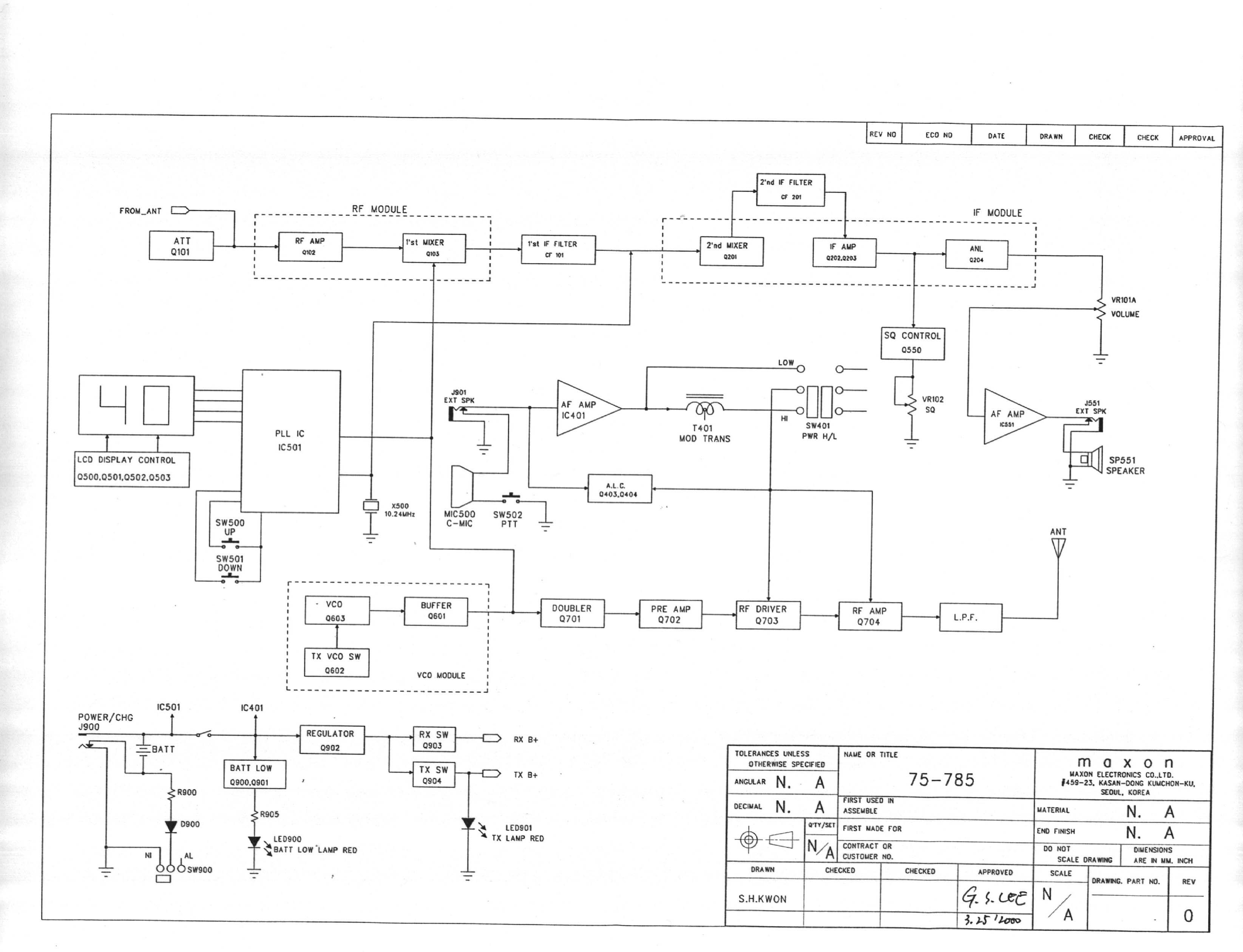
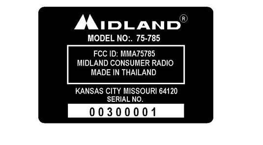
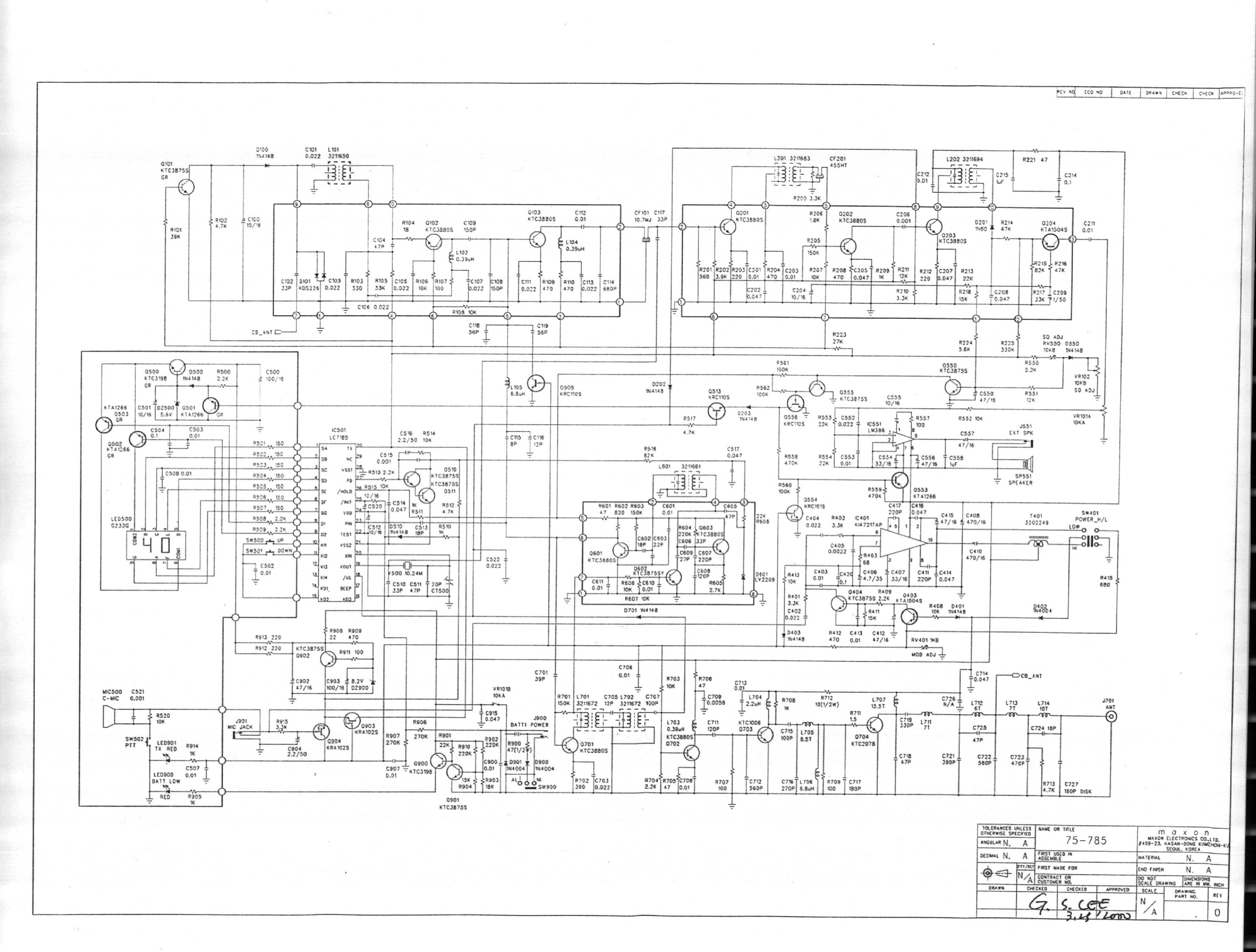
ENGINEERING STATEMENT For Type Certification of Midland Consumer Radio Model No: 75-785 FCC ID: MMA75785 I am an Electronics Engineer, a principal in the firm of Hyak Laboratories, Inc., Springfield, Virginia. My education and experience are a matter of record with the Federal Communications Commission. Hyak Laboratories, Inc. has been authorized by Midland Consumer Radio to make type certification measurements on the 75- 785 transceiver. These tests were made by me or under my supervision in our Springfield laboratory. Test data and documentation required by the FCC for type certification are included in this report. It is submitted that the above-mentioned transceiver meets all applicable FCC require- ments. ______________________________ Rowland S. Johnson Dated: April 14, 2000 A. INTRODUCTION The following data are submitted in connection with this request for type certification of the 75-785 transceiver in accordance with Part 2, Subpart J of the FCC Rules. The 75-785 is a double sideband amplitude modulated trans- mitter/receiver combination intended for battery operated hand- held operation in the citizens radio service. The transmitter has 40-channel capability in the 26.965 - 27.405 MHz band utilizing phase locked loop (PLL) technology. B. GENERAL INFORMATION REQUIRED FOR TYPE CERTIFICATION (Paragraph 2.983 of the Rules) 1. Name of applicant: Midland Consumer Radio 2. Identification of equipment: FCC ID: MMA75785 a. The equipment identification label is submitted as A separate exhibit. b. Photographs of the equipment are submitted as a separate exhibit. 3. Quantity production is planned. 4. Technical description: a. 6k00A3E emission b. Frequency range: 26.965 - 27.406 MHz c. Operating power of transmitter is fixed at the factory at less than 4 watts, and can be reduced 6 dB. d. Maximum power rating under 95.635(c) of the Rules is 4 watts. e. The dc voltage and dc currents at final amplifier: Collector voltage: 12.6 V Collector current: 610 mA @ 13.8 Vdc input. f. Function of each active semiconductor device: See Appendix 1. g. Complete circuit diagram is submitted as a separate exhibit. h. A user instruction book is submitted as a separate exhibit. i. The transmitter tune-up procedure is submitted as a separate exhibit. 2 B. GENERAL INFORMATION...(C j. A description of circuits for stabilizing frequency is included in Appendix 2. k. A description of circuits and devices employed for suppression of spurious radiation and for limiting modulation is included in Appendix 3. l. Not applicable. 5. Data for 2.985 through 2.997 follow this section. 6. RF_Power_Output (Paragraph 2.985(a),(b)(1) of the Rules) RF power output in the AM mode was measured with a Bird 4421 RF power meter and a Narda 765-20 50 ohm dummy load. (The transmitter was tuned by the factory.) Power was measured with a supply voltage of 13.8 volts, and indicated: Channel Power, watts HI LO 1 4.0 1.0 21 3.9 1.0 40 3.8 0.9 C. MODULATION CHARACTERISTICS 1. AF_Frequency_Response A curve showing frequency response of the transmitter is shown in Figure 1. Reference level was taken as a 1 kHz tone with 50% modulation, as measured on a Data Tech 209 modulation meter, using a Audio Precision TRMS voltmeter and tracking generator. 2. Modulation_Limiting Curves of AM modulation limiting for both positive and negative peaks are shown in Figures 2a and 2b, respectively. Characteristics at 300, 920, and 2500 Hz are shown using a Data Tech 209 modulation meter. Signal level was established with a Audio Precision TRMS voltmeter and tracking generator. The curves show compliance with Paragraph 95.633(d) of the Rules. 3 3. Modulation_Limiter_Attack_Time Modulation limiter attack time was measured by applying to the microphone input terminals a pulsed tone at 2500 Hz, 16 dB above the level required for 50% modulation at the frequency of maximum response, 920 Hz. The spectrum analyzer was tuned to upper and lower fourth- order sidebands in the time domain. Horizontal sweep of the analyzer was triggered in synchronism with the tone turn-on. Sweep speed was 100 milliseconds per division. Plots are included as Figures 3a and 3b. Any transients observed in excess of 33 dB attenuation as referenced to the carrier were less than 20 ms in duration. 4 FIGURE 1 TRANSMITTER FREQUENCY RESPONSE TRANSMITTER FREQUENCY RESPONSE FCC ID: MMA75785 FIGURE 1 5 FIGURE 2a AM MODULATION LIMITING - POSITIVE PEAKS MODULATION LIMITING CHARACTERISTICS Percent modulation as a function of input level at microphone jack in dBm for 300 Hz, 920 Hz, and 2500 Hz tones. MODULATION LIMITING POSITIVE PEAKS FCC ID: MMA75785 FIGURE 2a 6 FIGURE 2b AM MODULATION LIMITING - NEGATIVE PEAKS MODULATION LIMITING CHARACTERISTICS Percent modulation as a function of input level at microphone jack in dBm for 300 Hz, 920 Hz, and 2500 Hz tones. MODULATION LIMITING NEGATIVE PEAKS FCC ID: MMA75785 FIGURE 2b 7 FIGURE 3a MODULATION LIMITER ATTACK TIME Measurement_Conditions: 16 dB over 50% modulation level at 920 Hz with 2500 Hz tone, upper fourth order sideband; horizontal scale 100 ms/div. UPPER FOURTH-ORDER SIDEBAND LIMITER ATTACK TIME FCC ID: MMA75785 FIGURE 3a 8 FIGURE 3b MODULATION LIMITER ATTACK TIME Measurement_Conditions: 16 dB over 50% modulation level at 920 Hz with 2500 Hz tone, lower fourth order sideband; horizontal scale 100 ms/div. LOWER FOURTH-ORDER SIDEBAND LIMITER ATTACK TIME FCC ID: MMA75785 FIGURE 3b 9 C. MODULATION CHARACTERISTICS (Continued) 4. Occupied_Bandwidth_-_AM (Paragraph 2.989(c) of the Rules) Figures 4a and 4b are plots of the sideband envelope of the transmitter at low and high power settings respectively taken from a Tektronix 494P spectrum analyzer. Modulation corresponded to conditions of 2.989(a) and consisted of 2500 Hz tone at an input level 16 dB greater than that necessary to produce 50% modulation at 920 Hz, the frequency of maximum response. Measured modulation under these conditions was 87% positive, 85% negative. The plots are within the limits imp…
Text truncated - open the document above for the full version.
Contact Information
Applicant
Butch Rittmann(Director of Operations)
Technical Contact
Hyak Laboratories, Inc.Rowland S Johnson
[email protected](703) 451-1188
7011 Calamo St., Suite 107 · Springfield, Virginia · United States
Non-Technical Contact
Hyak Laboratories, Inc.Georgia Hall
[email protected](703) 451-1188
Test Firm
Hyak Laboratories, Inc.Rowland Johnson
703-451-1188
Technical Specifications
| # | Rule Parts | Frequency Range | Power Output | Emission | Tolerance |
|---|---|---|---|---|---|
| 2 | 95D | 26.965 MHz - 27.405 MHz | 4 W | 6K00A3E | 0.005 % |
Other Applications from Midland Radio Corporation
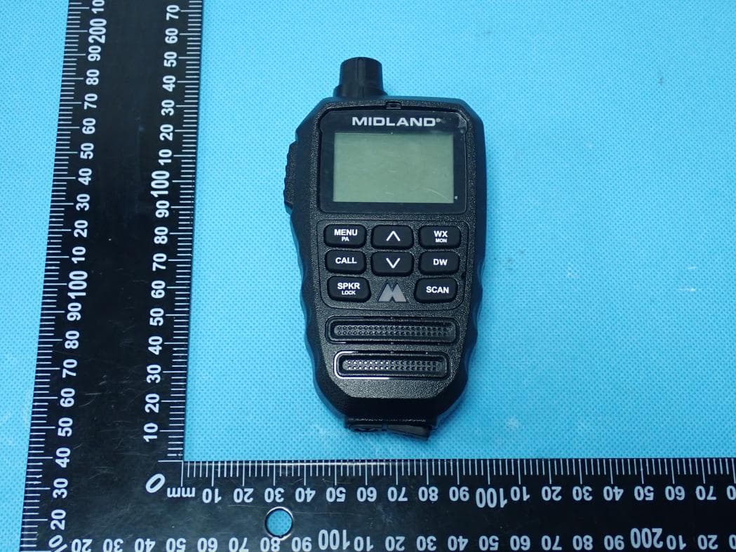
MMAMXMC95
Jun 10, 2026Wireless Bluetooth Microphone
Equipment Class
JAB - Part 15 Class B Digital Device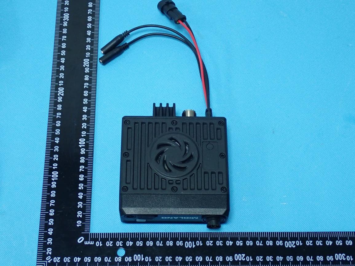
MMAMXT295
Jun 08, 2026GMRS Radio
Equipment Class
TNF - Licensed Non-Broadcast Transmitter Held to Face
MMACLIPTALK
Apr 27, 2026Transceiver
Equipment Class
DTS - Digital Transmission System
MMABR200S
Jan 13, 2026BUSINESS BAND TWO-WAY RADIO
Equipment Class
TNF - Licensed Non-Broadcast Transmitter Held to Face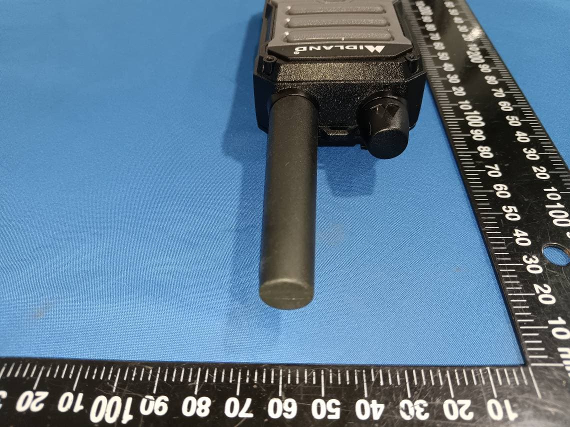
MMAGXT67
Oct 29, 2023GMRS RADIO
Equipment Class
TNF - Licensed Non-Broadcast Transmitter Held to Face