MMA9110RXARECEIVER
Midland Radio Corporation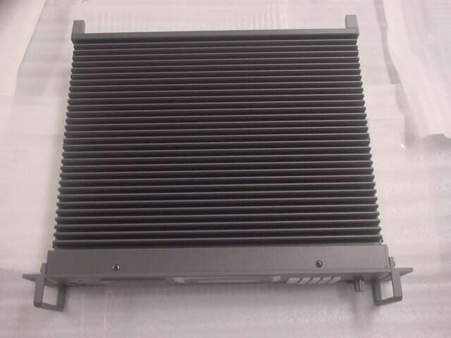
Click to zoom
Application Details
- Equipment Class
- CRR - Superregenerative Receiver
- Date of Grant
- Jul 22, 2010
- Application Purpose
- Original Equipment
- Date of Application
- Jul 22, 2010
- Equipment Note
- RECEIVER
- Frequency Range
- 136.00000000 - 156.00000000
- Company
- Midland Radio Corporation
- Country
- United States
Documents & Files
Document Text
Text extracted from the exhibit documents filed with the FCC. Open a document above to read the original.
Users Manual
www.midlandradio.com Operations Manual for the P25 Base Tech III Base/Repeater Station January 2009 Version 5.1 680-090-2042 2 www.midlandradio.com Version 5.1 680-090-2042 THE MANUFACTURER IS NOT RESPONSIBLE FOR ANY RADIO OR TV INTERFERENCE CAUSED BY UNAUTHORIZED MODIFICATIONS TO THIS EQUIPMENT. SUCH MODIFICATIONS COULD VOID THE USER'S AUTHORITY TO OPERATE THE EQUIPMENT. 3 www.midlandradio.com Version 5.1 680-090-2042 Introduction We thank you for choosing the Midland P25 Base Tech III Base/Repeater Station to meet your communication needs. Properly used, this product will give you many years of reliable service. To get the most out of your purchase, be sure to carefully read this manual before operating the radio. The overall operation of this radio depends entirely on how it has been programmed. If it is not functioning as desired, please check the programming first. This manual covers up to firmware version 71BS283 and 71CPV012 If you should need Midland Technical Support, please call 1-816-462-0463 or [email protected] Other useful Midland numbers; Main Line- 816-241-8500 Main Fax- 816-241-5713 LMR Sales- 816-462-0462 Credit Dept- 816-462-0464 Technical Support and Engineering Fax- 816-241-3272 Warranty Service- 816-462-0438 We welcome any comments on how we may improve our products to better server our customers. ______________________________________________________________________________ WARNING: The antenna(s) used for this transmitter must be fixed-mounted on outdoor permanent structures with a separation distance of at least 6 meters from all persons during normal operation. The peak conducted output power at each antenna terminal must not exceed 250 Watts and the peak radiated output power must not exceed 1000 Watts EIPR. Users and installers must ensure that FCC requirements for satisfying RF exposure compliance are met. (See FCC Rules Part 1, Sections 1307 and 1310) NOTICE: The AMBE+2 ™ voice coding Technology embodied in this product is protected by intellectual property rights including patent rights, copyrights and trade secrets of Digital Voice Systems, Inc. This voice coding Technology is licensed solely for use within this Communications Equipment. The user of this Technology is explicitly prohibited from attempting to extract, remove, decompile, reverse engineer or disassemble the Object Code, or in any other way convert the Object Code into a human readable form. U.S. Patents Nos. #5,870,405, #5,826,222, #5,754,974 #5,701,390, #5,715,365, #5,649,050, #5,630,011, #5,581,656, #5,517,511, #5,491,772, #5,247,579, #5,226,084 and #5,195,166. 4 www.midlandradio.com Version 5.1 680-090-2042 Table of Contents Page 1. LCD Display 4 2. LED Display 4 3. Key Controls 5 4. Programming 6 5. Control Knob 6 6. Channel Selection 7 7. P25 Calling Selection 8 8. P25 PTT Mode 9 9. P25 Conventional Messages 10 10. P25 Squelch Adjustment 16 11. Talk Group ID Alias 16 12. Key lock 17 13. Manual CWID Start/Stop 18 14. DTMF Encode 18 15. Analog Channel Data 19 16. P25 Channel Data 19 17. Bar Graph/Channel Display 20 18. LCD Backlight Toggle 20 19. Changing TX Power 21 20. Caller ID 21 21. Emergency Call Reception 22 22. Repeat Mode 22 23. Base Mode 23 24. Remote Control 23 25. P25 Test Mode 24 26. Adjustment Mode 26 27. Key Test 28 28. Displaying Firmware Version 29 29. Displaying Serial Number 29 30. Displaying Program Software Ver 30 31. Data Check 30 32. Error Messages 31 33. Firmware Error Detection 31 34. RS232 Error Detection 31 35. DSP Error Detection 32 36. Option Port Pinout 33 5 www.midlandradio.com Version 5.1 680-090-2042 1. LCD DISPLAY 1.1 LCD display consists of 4 x 20 characters as shown. Line 1: The Incoming RSSI with 10 steps Line 2: The output power levels with 10 steps Line 3: The left 4 letters show channel numbers. The middle 8 letters shows the channel name (if not programmed, it will be blank). The right 4 letters displays the status of the radio as described below. a. RX mode: M= Mix, both analog and digital can be received D= Only digital can be received. b. TX mode: D=PTT digital transmission A=PTT analog transmission c. Monitor mode: = Monitor off S= Selective squelch d. P-25 squelch: N= Normal squelch S= Selective squelch e. Low Voltage Icon: = Low Voltage state (Icon flashes with ALM LED) f. Key lock mode: =Key lock (Not displayed if in Low Voltage alarm) g. Shift mode: SHIFT KEY ICON (reverts to normal within 2 seconds) Line 4: The left 2 letters show GPC (GROUP CALL), AC (ALL CALL), IC (INDIVIDUAL CALL). The right 18 letters displays the GROUP NAME, INDIVIDUAL NUMBERS, ETC. RX = = = = = = = = = = TX = = = = = = = = = = C001 TAC 2 MDN GPC 500 2. LED DISPLAY The Midland Base Tech III has 5 LED's From left to right; DIGI= The LED is on when receiving a digital signal REP= The LED is on when in repeat mode. (The BASE TECH III can be programmed for, SIMPLEX -SEMIDUPLEX - DUPLEX- REPEATER on a per channel basis.) ALM= The LED flashes when an error on either TX or RX occurs TX= The LED is on when in Transmit BUSY= The LED is on when receiving a signal. 3. KEY CONTROLS 6 www.midlandradio.com Version 5.1 680-090-2042 3.1 Key entry without SHIFT key 0-9: channel numbers and individual call address (target address) A: P-25 calls (Group Call, All Call, and Individual Call) B: The beginning and the end of individual call number C: TX Transmit mode (Clear or Secure), only models with encryption. D= P-25 mode (analog or digital TX) *= Cancel channel number, individual number #= Ending channel number, individual number CH= Channel number entry, depress CH, then 0-9 for channels F (Scan) = P25 Conventional Control Messages (SBC) MON= monitor ON or OFF Rotary knob: Volume, Squelch, Back Light Dimmer and Timer 3.2 Key entry following SHIFT key 0= P-25 test mode start and finish 1=Backlight ON/OFF 2=TX power Hi/LOW 3=Talkaround ON/OFF 4=Change 5=No function 6=No function 7=Indicates Analog channel data 8=Key lock ON/OFF 9=No function A=Manual CWID sen…
Text truncated - open the document above for the full version.
External Photos
FRONT RIGHT SIDE LEFT SIDE BACK BOTTOM TOP
ID Label/Location Info
MIDLAND MODEL NO. 91-10RXA SERIAL NO. YYMMXXXX FCC ID: MMA9110RXA MADE IN JAPAN THIS DEVICE COMPLIES WITH PART 15 OF THE FCC RULES. OPERATION IS SUBJECT TO THE FOLLOWING TWO CONDITIONS: (1) THIS DEVICE MAY NOT CAUSE HARMFUL INTERFERENCE, AND (2) THIS DEVICE MUST ACCEPT ANY INTERFERENCE RECEIVED, INCLUDING INTERFERENCE THAT MAY CAUSE UNDESIRED OPERATION.
Internal Photos
RX UNIT
Operational Description
6.0 CIRCUIT DESCRIPTION 6.1 RECEIVER 1) RF Section An incoming signal is fed to pre-selector, and amplified by Q861, then fed to post-selector. The balanced mixer, consisting of IC811 produces 48.5MHz by injection from the 1 st local signal provided by Rx VCO. 2) IF Section The output signal from the mixer is fed to the crystal filter (XF801), then amplified by Q810. Again, this signal is fed to the 4-pole crystal filters and amplified by Q001. After amplified by Q001, signal is fed to the 2 nd IF processor (IC001). The 2 nd local crystal signal is fed to IC001 to produce the 2 nd local signal (455KHz). IC001 amplifies the 2 nd local signal and becomes an audio signal by detector circuit inclusive within IC001. Then, the audio signal is fed to the low-pass-filter inclusive in IC002, and fed to audio processor IC3. 3) VCO section The oscillator circuit produces the 1 st local signal (Rx frequency + 48.5MHz). The 1 st local signal is amplified by buffer (Q302), and again amplified by pre-amplifier (IC301) and post amplifier Q303. The amplified signal is fed to the balanced mixer. 4) PLL Section PLL IC inclusive with pre-scaller IC806 compares the phase between the VCO frequency and reference oscillator frequency (12.00MHz) by method of dividing the frequency, and produces VCO control signal. Then, this control signal is fed to the charge pump and fed to the low-pass-filter. The supply voltage of charge pump is multiplied by IC807 (approx. 13V) to achieve greater C/N ratio. 6.2 TRANSMITTER 1) VCO Section The oscillator circuit generates transmitter frequency. Then this signal is fed to the 3-stage of amplifier, buffer amplifier Q302, pre-amplifier IC301
Schematics
5V 7V 12V GNDLEN/WNC D867 HVU131 820ΩR867 C8933P 100PC810 10KR816 5P C811 10KR814 R8124.3K R84318K CKERRNC R87610K C8140.1μ 22nH L875L873 15nHL871 22nHC897 27P 2.5P C883C874 4PC865 3P 18P C840 VCO UNIT D803:B R817 15K 6.8KR834 1200 R859100K +12V IF UNIT +12VDSC.OUTSQ CONTRSSIRX/SWDATATURN FLC102 R857 15nH L874 27K L872 15nHL861 47nH 8P C898 1P C891C875 8P A C861 100PC869 2.5P LQW31H 33n L861 D868 HVU131 C8644P C8652P C8801nR863100K 1SV232 D862 1SV232 D863 L872 KQ0603 10n C87233P C8681.5P C8691.5P 0.1μC819 C818 47n 3 21 4 5 IC808TC4S66F2.7KR829 C821 ※ R8641K 15K R865 10KR869 C8753P C8781n C8742.5P C81515n 10nC820 DA204UD803:AR8261.2K R8271.2K R830100Ω D804:B C82210μ 10μC823 1nC851 10nC852 BLM21BL861 C8791n R86847Ω ※ C883 R86656Ω KQ1008L8650.68μ C882100P R82339K 47ΩR825 Q806 RTU002P02 100KR831 BL804HM501 R85410K R872100K 1SV232 D864 D865 1SV232 C88933P C88739P C8861P C8850.75P R818 18K 15KR819 Q809 2SD2351 C82510μ 10μC826 C829 3P C8921n 100KR875 10KR815 R83647K 100KR835 100KR838 TP801 23n LQW31H L876 56PC861 C86215P BLM21BL808 C808 10n C8120.33μ 4 13 25 TA75S01F IC809 BL806BLM21 5 4 123 #3060T803 R85810Ω C8130.15μC85510P C8584.7μ R84915Ω C84615P 3 2 1 4 5 #3060T802 1n C848 R851100Ω C847 1n 10nC856R81110K C8331n 150KR844 KQ1008 L8074.7μ 5 4 231 #3060T801 10μC803 C8320.1μ 2.2KR842 3 2 5 MF48QXF801 11PC837 C8389P C8011μ R807100K D8011SS355 R80847K D8091SS355 2SK508 Q810 R8464.7K L803KQ10081.5μC8541n R84815Ω 設計 470ΩR801 2.7nC804 R803100K 5.6KR802 8.2nC805 R82082K BL802 BLM21 220K R806 名称 図番 BL801HM501 +12VBUSY CN801 4A-S587 10KR855 C8637P L871 KQ0603 15n 150PC871 R870100K 1 53 4 2 Q808UMC2N 0Ω LQW18A L864 GRM42※C816 BL805BLM21 0Ω LL2012-F L866 2SK3018Q807 R82427Ω 1SS355 D805 120PC888 R87410K 2SK3018Q805 L80147nH R83339K C84015P C891※ 24PC897 C82810μ L875 KQ0603 15n BL809BLM21 0.33μC809 R860 1K SML-210VT D808 R81310K C8071μ GRM40 15 62 4 3 IC811 SPM5001 4 2 3 1 5 IC810 XC221A C8431μGRM40 C8411n C84410n C8451n Q803MCH3306 R85630K C8421μGRM40 C8361n 2SK3018Q801 R845100Ω R847270Ω C8341n 承認 検図 R8056.8K R8046.8K BL807HM501 ※ E558CNA-100035 L862 E558CNA-100035 L863 16151413121110 456789321 CN802 12.00MHz C8391n 146MHz---174MHz 71RXV6Y / 71RXV67-1 R82847K R862100K R87110K C8531n C87033P R82227KR82118K 4 85 1 IC807 NJU7662 R8324.7K D804:A DA204U C82410μC827 2.2μ/16V RB886G D806 21CS802 C8301n R873100K C8771n ※ C876 D866 1SV232 10nL873 KQ0603 L874 KQ0603 10n 6PC898 IC803 TC7W125FU IC804 TC7W125FU BLM21BL803 D8071SS355 R8403.3K C831 47n R85712K R850270Ω C84915P 1μKQ1008L806 R85347Ω 100Ω R852 製図 1 3 IC801 BA70BC0FP C8024.7μ C806 10n DTA144EUAQ811 R80947K 21 CS803 KQ1008 1.5μL809 C835 ※ RX UNIT CIRCUIT DIAGRAM KG710-15B 2A-SG0105-4 協同通信機製造株式会社 0.68μGRM42C817 C85722n R8610Ω Q861 3SK177 D802 1SS355 1 53 4 2 Q804UMC2N 1 2 IC805 XC6202P502M 100KR837 R839470Ω 82KR841 4 2 3 5 1 IC802 XC221A 1200 15KR810 L805 KQ1008 1μ L869 E558CNA-100036 L867 E558CNA-100035 L868 E558CNA-100035 1 Cont 2 GND 4 Vcc 3 Out TCXO801TCCAP 1.5ppm 6 1 CS801 1 7 CS804 1 2 IC812 XC6202P502M 20 11 10 1 MB1511 IC806 Q802 2SD2351
Test Report
FCC PART 15 B SUBPART B RECEIVER TEST REPORT Applicant MIDLAND RADIO CORPORATION Address 5900 PARRETTA DRIVE KANSAS CITY MISSOURI 64120 USA FCC ID MMA9110RXA Product Description RECEIVER Date Sample Received 7/1/2010 Date Tested 7/13/2010 Tested By Joe Scoglio Approved By Mario R. de Aranzeta Report Number 1593UT10TestReport.doc Test Results PASS FAIL THE ATTACHED REPORT SHALL NOT BE REPRODUCED EXCEPT IN FULL WITHOUT THE WRITTEN APPROVAL OF TIMCO ENGINEERING, INC. 849 NW State Road 45 Newberry, Fl 32669 USA Phone: 888.472.2424 or 352.472.5500 Fax: 352.472.2030 Email: [email protected] Website: www.timcoengr.com Certificate # 0955-01 APPLICANT: MIDLAND RADIO CORPORATION FCC ID: MMA9110RXA REPORT: M\MidlandRadio_MMA\1593UT10\1593UT10TestReport.doc Page 2 of 10 rev 2 mdea 09.20.2008 TABLE OF CONTENTS GENERAL REMARKS.............................................................................................................. 3 REPORT SUMMARY ............................................................................................................... 4 TEST ENVIRONMENT ............................................................................................................. 4 TEST SETUP SUMMARY ......................................................................................................... 4 DUT SPECIFICATION ............................................................................................................. 5 TEST EQUIPMENT LIST.......................................................................................................... 6 TEST PROCEDURES .............................................................................................................. 7 RADIATED SPURIOUS EMISSIONS ......................................................................................... 8 POWER LINE CONDUCTED INTERFERENCE .......................................................................... 9 RADIATED EMISSIONS TEST SETUP PHOTO ....................................................................... 10 APPLICANT: MIDLAND RADIO CORPORATION FCC ID: MMA9110RXA REPORT: M\MidlandRadio_MMA\1593UT10\1593UT10TestReport.doc Page 3 of 10 rev 2 mdea 09.20.2008 GENERAL REMARKS The attached report shall not be reproduced except in full without the written permission of Timco Engineering Inc. The test results relate only to the items tested. Summary The device under test does: fulfill the general approval requirements as identified in this test report not fulfill the general approval requirements as identified in this test report Attestations This equipment has been tested in accordance with the standards identified in this test report. To the best of my knowledge and belief, these tests were performed using the measurement procedures described in this report. All instrumentation and accessories used to test products for compliance to the indicated standards are calibrated regularly in accordance with ISO 17025 requirements. Certificate # 0955-01 I attest that the necessary measurements were made, under my supervision, at: Timco Engineering Inc. 849 NW State Road 45 Newberry, Fl 32669 Authorized Signatory Name: Mario de Aranzeta C.E.T. Compliance Engineer/ Lab. Supervisor Date: 7/13/2010 APPLICANT: MIDLAND RADIO CORPORATION FCC ID: MMA9110RXA REPORT: M\MidlandRadio_MMA\1593UT10\1593UT10TestReport.doc Page 4 of 10 rev 2 mdea 09.20.2008 REPORT SUMMARY Disclaimer The test results only relate to the item tested. Applicable Rule(s) Pt 15.109, Pt 15.107, ANSI C63.4: 2003 Related Report None TEST ENVIRONMENT Test Facility Timco Engineering, Inc. 849 NW State Road 45 Newberry, FL 32669 USA. Test Condition in the laboratory Temperature: 26ºC Relative humidity: 50% TEST SETUP SUMMARY Test Setup Diagram/ Description The DUT was placed on the turntable per setup per ANSI C63.4: 2003. A test set up photo is provided for clarification. Deviation from the standard/procedure No deviation Modification of DUT No modification APPLICANT: MIDLAND RADIO CORPORATION FCC ID: MMA9110RXA REPORT: M\MidlandRadio_MMA\1593UT10\1593UT10TestReport.doc Page 5 of 10 rev 2 mdea 09.20.2008 DUT SPECIFICATION DUT Description RECEIVER FCC ID MMA9110RXA DUT Power Source 110–120Vac/50– 60Hz DC Power Battery Operated Exclusively Test Item Prototype Pre-Production Production Type of Equipment Fixed Mobile Portable Laboratory Test Conditions Temperature: 26ºC Humidity: 55% Modifications to DUT: No Yes (explanation below) APPLICANT: MIDLAND RADIO CORPORATION FCC ID: MMA9110RXA REPORT: M\MidlandRadio_MMA\1593UT10\1593UT10TestReport.doc Page 6 of 10 rev 2 mdea 09.20.2008 TEST EQUIPMENT LIST Device Manufacturer Model Serial Number Cal/Char Date Due Date 3-Meter Semi- Anechoic Chamber Panashield N/A N/A Listed 03/10/10 03/10/12 Analyzer Tan Tower Quasi-Peak Adapter HP 85650A 3303A01690 CAL 11/22/09 11/22/11 Analyzer Tan Tower RF Preselector HP 85685A 3221A01400 CAL 11/21/09 11/21/11 Analyzer Tan Tower Spectrum Analyzer HP 8566B Opt 462 3138A07786 3144A20661 CAL 11/24/09 11/24/11 Analyzer Tan Tower Preamplifier HP 8449B-H02 3008A00372 CAL 11/21/09 11/21/11 Coaxial Cable #64 Semflex Inc. 60637 Timco #64 CHAR 3/30/09 3/30/11 Antenna: Dipole Kit Electro-Metrics TDA-30/1- 4 152 CAL 3/3/09 3/3/12 Antenna: Dipole Kit Electro-Metrics TDA-30/1- 4 153 CHAR 4/5/09 4/5/12 Hygro- Thermometer Extech 445703 0602 CAL 1/30/09 1/30/11 Modulation Analyzer HP 8901A 3435A06868 CAL 5/9/09 5/9/11 Digital Multimeter Fluke FLUKE-77- 3 79510405 CAL 5/14/09 5/14/11 APPLICANT: MIDLAND RADIO CORPORATION FCC ID: MMA9110RXA REPORT: M\MidlandRadio_MMA\1593UT10\1593UT10TestReport.doc Page 7 of 10 rev 2 mdea 09.20.2008 TEST PROCEDURES Power line conducted Emission: The test procedure used was ANSI C63.4-2003. The spectrum was scanned from 0.15 to 30 MHz. Radiation Interference: The test procedure used was ANSI C63.4-2003 using a spectrum analyzer with a preselector. The bandwidth of the spectrum analyzer was 100 kHz with an appropriate sweep speed. The analyzer was cal…
Text truncated - open the document above for the full version.
Contact Information
Applicant
Butch Rittmann(Director of Operations)
Test Firm
Timco Engineering, Inc.Bruno Clavier
Technical Specifications
| # | Rule Parts | Frequency Range | Power Output |
|---|---|---|---|
| 1 | 15B | 136 MHz - 156 MHz | - |
Other Applications from Midland Radio Corporation
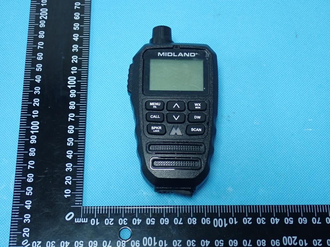
MMAMXMC95
Jun 10, 2026Wireless Bluetooth Microphone
Equipment Class
JAB - Part 15 Class B Digital Device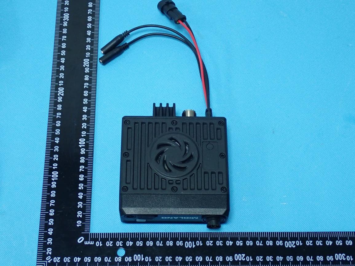
MMAMXT295
Jun 08, 2026GMRS Radio
Equipment Class
TNF - Licensed Non-Broadcast Transmitter Held to Face
MMACLIPTALK
Apr 27, 2026Transceiver
Equipment Class
DTS - Digital Transmission System
MMABR200S
Jan 13, 2026BUSINESS BAND TWO-WAY RADIO
Equipment Class
TNF - Licensed Non-Broadcast Transmitter Held to Face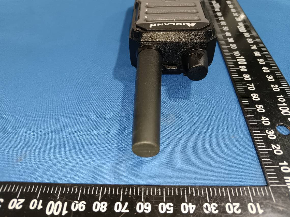
MMAGXT67
Oct 29, 2023GMRS RADIO
Equipment Class
TNF - Licensed Non-Broadcast Transmitter Held to Face