MMALXT118PAGMRS/ FRS
Midland Radio Corporation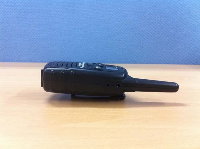
Click to zoom
Application Details
- Equipment Class
- FRF - Part 95 Family Radio Face Held Transmitter
- Date of Grant
- Sep 07, 2015
- Application Purpose
- Original Equipment
- Date of Application
- Sep 07, 2015
- Equipment Note
- GMRS/ FRS
- Frequency Range
- 467.56250000 - 467.71250000
- Company
- Midland Radio Corporation
- Country
- United States
Documents & Files
Document Text
Text extracted from the exhibit documents filed with the FCC. Open a document above to read the original.
Users Manual
Welcome to the world of Midland electronicsCongratulations on your purchase of a high quality MIDLAND product. Your2-way radio represents state-of-the-art high-tech engineering. Designed forGMRS (General Mobile Radio Service) operation, this compact package isbig on performance. It is a quality piece of electronic equipment, skillfullyconstructed with the finest components. The circuitry is all solid-state andmounted on a rugged printed circuit board. Your two-way radio is designedfor reliable and trouble-free performance for years to come.LCD DISPLA Y 1. TRANSMIT (TX) ICON – Indicates radio is transmitting a signal. 2. VOLUME METER – Indicates the volume setting of the radio. 3. RECEIVE (RX) ICON – Indicates radio is receiving a transmission. 4. LOW BATTERY ICON – Indicates the battery level is low. 5. VOX ICON – Indicates when VOX mode is active. 6. CHANNEL NUMBER – Changes from 1~22 on GMRS/FRS band. 1 CONTR OLS 7. PTT Button – Press and hold to transmit voice communication. 8. SCAN/LOCK Button – Press to enter SCAN mode. Press and hold to turnKEY LOCK on/off. 9. UP s and DOWN t Buttons – Make adjustments in MENU mode. 10. SPEAKER – Built-in speaker. 11. ANTENNA12. EXTERNAL SPEAKER/MIC/CHG JACK 13. POWER / MODE Button – Press and hold for at least 3 seconds to turn theradio on/off. Press momentarily toaccess Menu mode. 14. MIC – Built-in microphone. This device complies with Part 15 of the FCC Rules. Operation is subject to thefollowing two conditions: (1) this device does not cause harmful interference, and (2) thisradio must accept any interference that may cause undesired operation.To maintain compliance with FCC’s RF exposure guidelines, for body-worn operation,this radio has been tested and meets the FCC RF exposure guidelines when used withMidland Radio Corp. accessories supplied or designated for this product. Use of otheraccessories may not ensure compliance with FCC RF exposure guidelines. 141312 11 10 98 7 654 32 IMPORTANT NOTICE, FCC LICENSE REQUIRED FOR GMRS OPERATION(Only Applicable for GMRS Radio Use in the United States)The radios operate on GMRS (General Mobile Radio Service) frequencieswhich require an FCC (Federal Communications Commission) license. Youmust be licensed prior to operating on channels 1 - 7 or 15 - 22, whichcomprise the GMRS channels of the radios. Serious penalties could resultfrom unlicensed use of GMRS channels, in violation of FCC rules, asstipulated in the Communications Acts Sections 501 and 502 (amended).You will be issued a call sign by the FCC which should be used for stationidentification when operating the radio on GMRS channels. You should alsocooperate by engaging in permissible transmissions only, avoiding channelinterference with other GMRS users, and being prudent with the length of yourtransmission time.To obtain a license or ask questions about the license application, contactthe FCC at 1-888-CALL FCC or go to the FCC's website: http://www .fcc.gov and request form 605 . Exposure To Radio Frequency EnergyYour Midland radio is designed to comply with the following national andinternational standards and guidelines regarding exposure of human beingsto radio frequency electromagnetic energy:- United States Federal Communications Commission, Code of Federal Regulations: 47 CFR part 2 sub-part J - American National Standards Institute (ANSI)/Institute of Electrical & Electronic Engineers (IEEE) C95. 1-1992 - Institute of Electrical and Electronic Engineers (IEEE) C95. 1-1999 Edition- National Council on Radiation Protection and Measurements (NCRP) of the United States, Report 86, 1986 - International Commission on Non-lonizing Radiation Protection (ICNIRP) 1998 To control your exposure and ensure compliance with the general populationor uncontrolled environment exposure limits, transmit no more than 50% ofthe time. The radio generates measurable RF energy exposure only whentransmitting. IMPORTANT: Changes or modifications to this unit not expressly approved by MIDLAND RADIO CORP. could void your right to operate this unit. Your radio is set up to transmit a regulated signal on an assigned frequency. It is againstthe law to alter or adjust the settings inside the COMMUNICATOR to exceedthose limitations. Any adjustment to your radio must be made by qualifiedtechnicians. MM II DD LL AA NN DD RR AA DD II OO CC OO RR PP OO RR AA TT II OO NN 5900 Parretta Drive Kansas City, MO 64120 Call 816.241.8500 We’d love to hear from you! Let us know what you think of your new Midland product on or by visiting us at midlandusa.com Note: Features & Specifications are subject to change withoutnotice. MIDLAND is not responsible for unintentional errors oromissions on its packaging. BA T TER Y INS T ALLA TION Your radio operates with 3 AAA alkaline batteries or NiMH rechargeablebatteries. The belt clip should be removed to ease installation or removalof the batteries. To install the batteries:1. With the back of the radio facing you, remove the belt clip (see diagram below) for easy access, then remove the Battery Cover by pressing down on the top center and sliding it down from the radio. 2. Insert 3 AAA batteries observing the polarity as shown on the Battery Compartment. Installing the batteries incorrectly will prevent the unit from operating or may damage the unit. 3. Return the Battery Cover by sliding it up on the radio. Replace the belt clip, making sure it locks into place. BATTERYCOMPARTMENT BATTERYCOMPARTMENTCOVER Press here and push down to open BELT CLIPLOCK TABBELT CLIP LATCH CHAR GING THE BA T TER Y Your radio is equipped for using rechargeable NiMH batteries which can berecharged by inserting the AC adapter into the radio charge jack. Initialcharge time is 24 hours. Charge time is about 12 hours thereafter. Formaximum battery life, we recommend charging the batteries when the lowbattery icon comes on. Remove the radios from the charger when thecharge time expires. 1. Only use our NiMH batteries.2. Do not attempt to charge alkaline batteries or …
Text truncated - open the document above for the full version.
Cover Letter(s)
Midland Radio Corporation 5900 Parretta Drive, Kansas City, Missouri United States 64120 Date: September 03, 2015 Federal Communications Commission Authorization and Evaluation Division Confidentiality Request regarding application for certification of FCC ID: MMALXT118PA Pursuant to Sections 0.457 and 0.459 of the Commission’s Rules, we hereby request confidential treatment of information accompanying this application as outlined below: Exhibit Type File Name Schematics Diagram(s) CONF APPENDIX_ LXT118PA_Schematics.PDF Block diagram CONF APPENDIX_ LXT118PA_Block diagram.PDF Operation description CONF APPENDIX_ LXT118PA_Operation description.PDF The above materials contain trade secrets and proprietary information not customarily released to the public. The public disclosure of these materials may be harmful to the applicant and provide unjustified benefits to its competitors. The applicant understands that pursuant to Section 0.457 of the Rules, disclosure of this application and all accompanying documentation will not be made before the date of the Grant for this application. Sincerely, Jeff Brame
External Photos
www.kes.co.kr FCC ID : MMALXT118PA Page 1 of 5 EUT External photographs www.kes.co.kr FCC ID : MMALXT118PA Page 2 of 5 www.kes.co.kr FCC ID : MMALXT118PA Page 3 of 5 www.kes.co.kr FCC ID : MMALXT118PA Page 4 of 5 www.kes.co.kr FCC ID : MMALXT118PA Page 5 of 5
ID Label/Location Info
Midland Radio Corporation 5900 Parretta Drive, Kansas City, Missouri United States 64120 September 03, 2015 Federal Communications Commission Equipment Authorization Branch 7435 Oakland Mills Road Columbia, MD 21046 SUBJECT : Midland Radio Corporation FCC ID : MMALXT118PA Label Justification Letter Dear Sir/Madame, Because the device is so small that it is not practicable to place the statement specified under 15.19 statement request, the information required by this paragraph shall be placed in a prominent location in the User’s Manual. - The available label area on the device is limited because it is relatively small and has many contoured surfaces, keypads, LDC display, and other connectors. - The batteries are designed for easy removal and the label will be visible whenever the batteries are removed for replacement. - The label will be readily visible at the time of purchase because the device will be marketed without the battery installed. - FCC ID will be printed on the gift box which will be readily visible to the purchaser at the time of purchase. Sincerely, Jeff Brame Midland Radio Corporation 5900 Parretta Drive, Kansas City, Missouri United States 64120 Label and Location
ID Label/Location Info
S/N
Internal Photos
www.kes.co.kr FCC ID : MMALXT118PA Page 1 of 2 EUT Internal photographs Helical Antenna www.kes.co.kr FCC ID : MMALXT118PA Page 2 of 2
Parts List/Tune Up Info
GLOBAL LINK CORP. LTD. LXT118PA Series - Bill of Material Dwg. No. : LXT118PA-BOM-M-05 Rev. Date: 11/06/15 C1 CHIP CAPACITOR 0402 NPO ±5%100P1 YageoYageo C10 CHIP CAPACITOR 0402 NPO ±5%100P1 YageoYageo C104 CHIP CAPACITOR 0402 NPO ±5%100P1 YageoYageo C11CHIP CAPACITOR 0402 X7R +/- 10%0.1UF (X7R)1YageoYageo C12 CHIP CAPACITOR 0603 Y5V1UF1 YageoYageo C122 CHIP CAPACITOR 0402 NPO ±5%100P1 YageoYageo C125 CHIP CAPACITOR 0402 X7R ±10%0.001UF1 YageoYageo C13 CHIP CAPACITOR 0402 NPO ±5%100P1 YageoYageo C133 CHIP CAPACITOR 0805 X5R ±10% 10UF/10V (05)1MurataAsung C14 CHIP CAPACITOR 0402 NPO ±5%100P1 YageoYageo C140CHIP CAPACITOR 0402 X7R +/- 10%470P(X7R)1YageoYageo C142 CHIP CAPACITOR 0402 NPO ±5%100P1 YageoYageo C144 CHIP CAPACITOR 0402 NPO ±5%100P1 YageoYageo C145 CHIP CAPACITOR 0402 X7R ±10%0.001UF1 YageoYageo C148 CHIP CAPACITOR 0402 NPO ±0.25PF 5P 1 YageoYageo C15 CHIP CAPACITOR 0402 NPO ±5%100P1 YageoYageo C16 CHIP CAPACITOR 0603 Y5V1UF1 YageoYageo C162 CHIP CAPACITOR 0402 NPO ±5%100P1 YageoYageo C166 CHIP CAPACITOR 0402 NPO ±5%100P1 YageoYageo C17 CHIP CAPACITOR 0603 NPO ±0.25PF 3P(03) 1 YageoYageo PA-LXT3-B0002 29-Jan-15 C172 CHIP CAPACITOR 0402 NPO ±5%100P1 YageoYageo C173 CHIP CAPACITOR 0402 NPO ±5%100P1 YageoYageo C174 CHIP CAPACITOR 0402 NPO ±5%100P1 YageoYageo C178 CHIP CAPACITOR 0402 NPO ±5%100P1 YageoYageo C179 CHIP CAPACITOR 0402 NPO ±5% 22P1YageoYageo C17A CHIP CAPACITOR 0402 NPO ±0.25PF 1P 1 YageoYageo C18 CHIP CAPACITOR 0603 Y5V2.2UF(03)1 YageoYageo C182 CHIP CAPACITOR 0402 NPO ±5%100P1 YageoYageo C19 CHIP CAPACITOR 0402 NPO ±5%100P1 YageoYageo C2 CHIP CAPACITOR 0603 NPO ±5% 100P(0603)1YageoYageo C20 CHIP CAPACITOR 0402 Y5V0.1UF1 YageoYageo C207 CHIP CAPACITOR 0402 NPO ±5%100P1 YageoYageo C208 CHIP CAPACITOR 0402 NPO ±5%33P1 YageoYageo C209 CHIP CAPACITOR 0402 NPO ±5%33P1 YageoYageo C21 CHIP CAPACITOR 0402 NPO ±0.25PF 7P 1 YageoYageo C22 CHIP CAPACITOR 0402 NPO ±5%100P1 YageoYageo C23 CHIP CAPACITOR 0402 NPO ±5%100P1 YageoYageo C24 CHIP CAPACITOR 0402 Y5V0.1UF1 YageoYageo C25 CHIP CAPACITOR 0402 Y5V0.1UF1 YageoYageo C26 CHIP CAPACITOR 0402 NPO ±5%100P1 YageoYageo C27 CHIP CAPACITOR 0805 X5R ±10% 10UF/10V (05)1MurataASKOPA-LXT3-B000511-Jun-15 C28 CHIP CAPACITOR 0603 Y5V1UF1 YageoYageo C29 CHIP CAPACITOR 0402 Y5V0.1UF1 YageoYageo C3 CHIP CAPACITOR 0402 X7R ±10%0.001UF1 YageoYageo C30 CHIP CAPACITOR 0603 NPO ±0.25PF 6P(03) 1 YageoYageo C304 CHIP CAPACITOR 0402 NPO ±0.25PF3P1 YageoYageo C31 CHIP CAPACITOR 0402 Y5V0.1UF1 YageoYageoPA-LXT3-B000511-Jun-15 C32 CHIP CAPACITOR 0402 Y5V0.1UF1 YageoYageoPA-LXT3-B000511-Jun-15 C33 CHIP CAPACITOR 0805 X5R ±10% 10UF/10V (05)1MurataAsung C34 CHIP CAPACITOR 0402 X7R ±10%0.01UF1 YageoYageoPA-LXT3-B000511-Jun-15 C35 CHIP CAPACITOR 0402 NPO ±5%100P1 YageoYageo C36 CHIP CAPACITOR 0402 X7R ±10%0.001UF1 YageoYageoPA-LXT3-B000511-Jun-15 C37 CHIP CAPACITOR 0402 NPO ±0.25PF 8P 1 YageoYageo C39 CHIP CAPACITOR 0402 NPO ±5%100P1 YageoYageo C3A CHIP CAPACITOR 0603 NPO ±0.25PF 2P(03) 1 YageoYageo PA-LXT3-B0002 29-Jan-15 C4 CHIP CAPACITOR 0402 NPO ±0.25PF3P1 YageoYageo PA-LXT3-B0002 29-Jan-15 C41 CHIP CAPACITOR 0402 NPO ±5%100P1 YageoYageo C43Elect capacitor 470UF/6.3v (6x7)470uF/6.3V 6x7mm1SamconSamconPA-LXT3-B000310-Mar-15 C44 CHIP CAPACITOR 0402 X7R ±10%0.0018UF1 YageoYageo C45 CHIP CAPACITOR 0402 NPO ±5%100P1 YageoYageo C46 CHIP CAPACITOR 0402 NPO ±5%100P1 YageoYageo C47 CHIP CAPACITOR 0402 NPO ±5%100P1 YageoYageo C48 CHIP CAPACITOR 0805 X5R ±10% 10UF/10V (05)1MurataAsung C49 CHIP CAPACITOR 0402 X7R ±10%0.01UF1 YageoYageo C5 CHIP CAPACITOR 0402 Y5V0.1UF1 YageoYageo C50 CHIP CAPACITOR 0603 Y5V1UF1 YageoYageo C51 CHIP CAPACITOR 0402 Y5V0.1UF1 YageoYageo C52 CHIP CAPACITOR 0402 Y5V0.1UF1 YageoYageo C53 CHIP CAPACITOR 0402 Y5V0.1UF1 YageoYageo C55CHIP CAPACITOR 0402 X7R +/- 10%0.1UF (X7R)1YageoYageo C56 CHIP CAPACITOR 0402 NPO ±5%100P1 YageoYageo C57 CHIP CAPACITOR 0402 X7R ±10%0.01UF1 YageoYageo C58 CHIP CAPACITOR 0402 Y5V0.1UF1 YageoYageo C59 CHIP CAPACITOR 0402 NPO ±5%10P1 YageoYageo C6 CHIP CAPACITOR 0603 NPO ±0.25PF 9P(03) 1 YageoYageo C60 CHIP CAPACITOR 0402 NPO ±5%100P1 YageoYageo C61 CHIP CAPACITOR 0402 NPO ±5%100P1 YageoYageo C62 CHIP CAPACITOR 0402 NPO ±5%100P1 YageoYageo C63 CHIP CAPACITOR 0402 Y5V0.1UF1 YageoYageo C64 CHIP CAPACITOR 0402 NPO ±0.25PF 7P 1 YageoYageo C65 CHIP CAPACITOR 0402 Y5V0.1UF1 YageoYageo C66 CHIP CAPACITOR 0402 NPO ±5%10P1 YageoYageo C67 CHIP CAPACITOR 0402 NPO ±5%100P1 YageoYageo C68 CHIP CAPACITOR 0402 NPO ±5%100P1 YageoYageo C69 CHIP CAPACITOR 0402 NPO ±5%18P1 YageoYageo C7 CHIP CAPACITOR 0402 NPO ±5%100P1 YageoYageo C70 CHIP CAPACITOR 0402 NPO ±5%100P1 YageoYageo C71 CHIP CAPACITOR 0402 NPO ±5%10P1 YageoYageo PA-LXT3-B0002 29-Jan-15 C72 CHIP CAPACITOR 0603 Y5V1UF1 YageoYageo C73 CHIP CAPACITOR 0402 X7R ±10%0.01UF1 YageoYageo C74 CHIP CAPACITOR 0402 NPO ±5%100P1 YageoYageo C76 CHIP CAPACITOR 0402 NPO ±5%100P1 YageoYageo C77 CHIP CAPACITOR 0402 X7R ±10%0.01UF1 YageoYageo C8 CHIP CAPACITOR 0402 NPO ±5%100P1 YageoYageo C80 CHIP CAPACITOR 0402 NPO ±5%100P1 YageoYageo C85 CHIP CAPACITOR 0402 Y5V0.1UF1 YageoYageo C9 CHIP CAPACITOR 0603 NPO ±0.25PF 10P(03) 1 YageoYageo C90 CHIP CAPACITOR 0402 Y5V0.1UF1 YageoYageo C93 CHIP CAPACITOR 0402 NPO ±5%100P1 YageoYageo C95 CHIP CAPACITOR 0402 NPO ±5%100P1 YageoYageo Remark1st Vendor ECO Ref.NoQ'tyManufacturerDescriptionItems Global Link Corporation Confidential Proprietary page1/3 GLOBAL LINK CORP. LTD. LXT118PA Series - Bill of Material Dwg. No. : LXT118PA-BOM-M-05 Rev. Date: 11/06/15 Remark1st Vendor ECO Ref.NoQ'tyManufacturerDescriptionItems C98 CHIP CAPACITOR 0402 Y5V0.1UF1 YageoYageo C997 CHIP CAPACITOR 0402 NPO ±0.25PF 2P 1 YageoYageo PA-LXT3-B0002 29-Jan-15 CMIC1Condensor MicF9745AP342-98 (RoHS)1InnovationInnovation CPU1 IC CPU (Flash)WT56F108 1WeltrendGL buy & sell D1 Chip Diode SwitchingKDS114E1KECEon D13 Chip Diode SwitchingKDS114E1KECEon D2 Chip Diode SwitchingKDS114E1KECEon D3SMT Schottky Barrier DiodeSM130A1 LRCLRC IC1Analog Radio ICBK48131BekenGL consign IC2IC Regulator 2.8V…
Text truncated - open the document above for the full version.
Parts List/Tune Up Info
1) Set the unit at channel 1.(462.5625MHz) Press the PTT button so the unit will be in transmit mode. 2)Adjust CT1 trimmer until Fc +/- 200Hz. 4. Maximum Audio Deviation 2) Go to Max. deviation alignment mode by press and holding the Call button then turn on the radio. 3. Transmitter Output Power at conducted condition. 3) TX power check the 24dBm +/- 1dBm. 1) TP(ALG) is short to GND. 1) Set the power supply at 3.6Vdc. Set the unit at GMRS ch 1.(462.5625MHz) and FRS ch 8. (467.5625MHz) 2) Press the PTT button so the unit will be in transmit mode. LXT118PA Alignment Procedure 2015. 08. 27. 1. VCO Alignment ; Fixed. 2. Transmitter Frequency Alignment 3) LCD become on display such as belows. Press the Up or Down button to align if necessory each step. Display Default value ① GMRS Maximum Deviation Alignment td 0b Test frequency ; 462.5625MHz ① GMRS Squelch Alignment gr 09 Test frequency ; 462.7125MHz 6. Memory clear by press and holding the Up button then turn on the radio. 5. Receiver Squelch Alignment 1) TP(ALG) is short to GND. 2) Go to RX squelch alignment mode by press and holding the Down button then turn on the radio. Display Default value 3) LCD become on display such as belows. Press the Up or Down button to align if necessory each step. 7. If TP(ALG) is short to GND, Alignment mode is enable. If TP(ALG) is open to GND, Alignment mode is disable.
RF Exposure Info
Test Lab System DUT: D Commun Medium Phantom Measure DASY4 Flat-Se Maximu Flat-Se dz=5mm Referenc Peak SA SAR(1 g Maximu boratory: KE m verificatio Dipole 450 M nication Sys m parameters m section: Fla ement Standa Configurati Probe: ES3 D Sensor-Surfa Electronics: Phantom: E L Measuremen ection_HSL um value of S ection_HSL m ce Value = 3 AR (extrapola g) = 1.2 mW um value of S ES Co., Ltd. on_450_HS MHz; Type: D tem: CW; Fr used: f = 45 at Section ard: DASY4 on: DV3 - SN331 face: 4mm (M DAE4 Sn13 LI v5.0_2013 nt SW: DAS L_450/Area SAR (interpo L_450/Zoom 37.7 V/m; Po ated) = 1.80 W/g; SAR(10 SAR (measu SL D450V3; Se requency: 45 0 MHz; σ = (High Preci 15; ConvF(6 Mechanical S 344; Calibrat 3_01_23; Ty Y4, V4.7 Bu a Scan (41x olated) = 1.24 m Scan (7x7 ower Drift = W/kg g) = 0.843 m red) = 1.27 m erial: D450V 50 MHz;Duty 0.833 mho/m sion Assessm 6.91, 6.91, 6.9 Surface Detec ted: 2014-11 ype: QDOVA uild 80; Postp x201x1): Me 4 mW/g 7x7)/Cube -0.101 dB mW/g mW/g Date V3 - SN:1081 y Cycle: 1:1 m; ε r = 43; ρ ment) 91); Calibrat ction) -12 A002AA; Ser processing S easurement g 0: Measurem e/Time: 2015 1 = 1000 kg/ m ted: 2015-05 rial: TP:1190 W: SEMCA grid: dx=15m ment grid: dx 5-08-28 AM m 3 -27 0 AD, V1.8 Bui mm, dy=15m x=5mm, dy= 10:44:08 ild 186 mm =5mm, Test Lab System DUT: D Commun Medium Phantom Measure DASY4 Flat-Se Maximu Flat-Se dz=5mm Referenc Peak SA SAR(1 g Maximu boratory: KE m verificatio Dipole 450 M nication Sys m parameters m section: Fla ement Standa Configurati Probe: ES3 D Sensor-Surfa Electronics: Phantom: E L Measuremen ection_MSL um value of S ection_MSL m ce Value = 3 AR (extrapola g) = 1.06 mW um value of S ES Co., Ltd. on_450_MS MHz; Type: D tem: CW; Fr used: f = 45 at Section ard: DASY4 on: DV3 - SN331 face: 4mm (M DAE4 Sn13 LI v5.0_2013 nt SW: DAS L_450/Area SAR (interpo L_450/Zoom 34.4 V/m; Po ated) = 1.61 W/g; SAR(1 SAR (measu SL D450V3; Se requency: 45 0 MHz; σ = (High Preci 15; ConvF(6 Mechanical S 344; Calibrat 3_01_23; Ty Y4, V4.7 Bu a Scan (41x olated) = 1.1 m Scan (7x ower Drift = 0 W/kg 0 g) = 0.723 red) = 1.13 m erial: D450V 50 MHz;Duty 0.899 mho/m sion Assessm 6.99, 6.99, 6.9 Surface Detec ted: 2014-11 ype: QDOVA uild 80; Postp x201x1): M 1 mW/g x7x7)/Cube 0.049 dB mW/g mW/g Date V3 - SN:1081 y Cycle: 1:1 m; ε r = 55.2; ment) 99); Calibrat ction) -12 A002AA; Ser processing S easurement g 0: Measure e/Time: 2015 1 ρ = 1000 k g ted: 2015-05 rial: TP:1190 W: SEMCA grid: dx=15m ment grid: dx 5-08-27 AM g/m 3 -27 0 AD, V1.8 Bui mm, dy=15m dx=5mm, dy= 11:57:47 ild 186 mm =5mm, Plot 1 Test Lab Head_G DUT: L Commun Medium kg/m 3 Phanto m Measure DASY4 Head_G dx=15m Info: In t Maximu Head_G grid: dx= Referenc Peak SA SAR(1 g Info: In t Maximu boratory: KE GMRS_An LXT118PA; nication Sys m parameters m section: Fla ement Standa Configurati Probe: ES3 D Sensor-Surfa Electronics: Phantom: E L Measuremen GMRS_An mm, dy=15mm terpolated me um value of S GMRS_An =5mm, dy=5 ce Value = 1 AR (extrapola g) = 0.232 m terpolated me um value of S ES Co., Ltd. nalog_25mm Type: Bar; tem: CW; F r used (interp at Section ard: DASY4 on: DV3 - SN331 face: 4mm (M DAE4 Sn13 LI v5.0_2013 nt SW: DAS nalog_25mm m edium param SAR (interpo nalog_25mm 5mm, dz=5m 16.6 V/m; Po ated) = 0.305 mW/g; SAR( edium param SAR (measu m Gap_462 Serial: N/A requency: 46 olated): f = 4 (High Preci 15; ConvF(6 Mechanical S 344; Calibrat 3_01_23; Ty Y4, V4.7 Bu m Gap_462 meters used fo olated) = 0.24 m Gap_462 mm ower Drift = 5 W/kg 10 g) = 0.17 meters used fo red) = 0.243 2.6375 A 62.637 MHz; 462.637 MH sion Assessm 6.91, 6.91, 6.9 Surface Detec ted: 2014-11 ype: QDOVA uild 80; Postp 2.6375/Area for SAR eval 48 mW/g 2.6375/Zoom -0.146 dB 79 mW/g for SAR eval mW/g Date ;Duty Cycle: Hz; σ = 0.843 ment) 91); Calibrat ction) -12 A002AA; Ser processing S a Scan (51x luation. m Scan (7x luation. e/Time: 2015 1:1 mho/m; ε r = ted: 2015-05 rial: TP:1190 W: SEMCA x111x1): Me x7x7)/Cube 5-08-28 AM = 42.8; ρ = 10 -27 0 AD, V1.8 Bui easurement g e 0: Measure 11:58:15 000 ild 186 grid: ement Plot 2 Test Lab Head_F DUT: L Commun Medium kg/m 3 Phanto m Measure DASY4 Head_F dx=15m Info: In t Maximu Head_F dx=5mm Referenc Peak SA SAR(1 g Info: In t Maximu boratory: KE FRS_Analo LXT118PA; nication Sys m parameters m section: Fla ement Standa Configurati Probe: ES3 D Sensor-Surfa Electronics: Phantom: E L Measuremen FRS_Analo mm, dy=15mm terpolated me um value of S FRS_Analo m, dy=5mm, ce Value = 1 AR (extrapola g) = 0.294 m terpolated me um value of S ES Co., Ltd. og_25mm G Type: Bar; tem: CW; F r used (interp at Section ard: DASY4 on: DV3 - SN331 face: 4mm (M DAE4 Sn13 LI v5.0_2013 nt SW: DAS og_25mm G m edium param SAR (interpo og_25mm G dz=5mm 19.6 V/m; Po ated) = 0.381 mW/g; SAR( edium param SAR (measu Gap_467.63 Serial: N/A requency: 46 olated): f = 4 (High Preci 15; ConvF(6 Mechanical S 344; Calibrat 3_01_23; Ty Y4, V4.7 Bu Gap_467.63 meters used fo olated) = 0.3 Gap_467.63 ower Drift = 1 W/kg 10 g) = 0.23 meters used fo red) = 0.306 375 A 67.637 MHz; 467.637 MH sion Assessm 6.91, 6.91, 6.9 Surface Detec ted: 2014-11 ype: QDOVA uild 80; Postp 375/Area S for SAR eval 14 mW/g 375/Zoom S -0.063 dB 0 mW/g for SAR eval 6 mW/g Da ;Duty Cycle: Hz; σ = 0.845 ment) 91); Calibrat ction) -12 A002AA; Ser processing S Scan (51x11 luation. Scan (7x7x luation. ate/Time: 201 1:1 mho/m; ε r = ted: 2015-05 rial: TP:1190 W: SEMCA 11x1): Meas 7)/Cube 0: 15-08-28 PM = 42.7; ρ = 10 -27 0 AD, V1.8 Bui surement grid Measureme M 2:22:58 000 ild 186 d: ent grid: Plot 3 Test Lab Body_G DUT: L Commun Medium kg/m 3 Phanto m Measure DASY4 Body_G dx=15m Info: In t Maximu Body_G dx=5mm Referenc Peak SA SAR(1 g Info: In t Maximu boratory: KE GMRS_An LXT118PA; nication Sys m parameters m section: Fla ement Standa Configurati Probe: ES3 D Sensor-Surfa Electronics: Phantom: E L Measuremen GMRS_An mm, dy=15mm terpolated me um value of S GMRS_An m, dy=5mm, ce Value = 2 AR (extrapola g) = 0.507 m terpolat…
Text truncated - open the document above for the full version.
RF Exposure Info
KES Co., Ltd. C-3701, Simin-daero 365-40, Dongan-gu, Anyang-si, Gyeonggi-do, 14057, Korea Tel: +82-31-425-6200 / Fax: +82-31-424-0450 www.kes.co.kr Test report No.: KES-SR-15T0022 Page (2 ) of (20) This report shall not be reproduced except in full, without the written approval of KES Co., Ltd. The test results in the report only apply to the tested sample. KES-P-5101-14 Rev. 1 KES A4 Revision history Revision Date of issue Test report No. Description - 2015.09.04 KES-SR-15T0022Initial KES Co., Ltd. C-3701, Simin-daero 365-40, Dongan-gu, Anyang-si, Gyeonggi-do, 14057, Korea Tel: +82-31-425-6200 / Fax: +82-31-424-0450 www.kes.co.kr Test report No.: KES-SR-15T0022 Page (3 ) of (20) This report shall not be reproduced except in full, without the written approval of KES Co., Ltd. The test results in the report only apply to the tested sample. KES-P-5101-14 Rev. 1 KES A4 TABLE OF CONTENTS 1. General information ................................................................................................................................................... 4 1.1. EUT description ........................................................................................................................................ 4 1.2. Short description of the equipment under test(EUT) ................................................................................. 4 1.3. Highest SAR summary .............................................................................................................................. 4 1.4. Guidance applied ....................................................................................................................................... 5 1.5. Test conditions ........................................................................................................................................... 5 1.6. SAR definition ........................................................................................................................................... 5 1.7. Accessories of EUT ................................................................................................................................... 6 2. SAR measurement system .......................................................................................................................................... 7 2.1. Robot ......................................................................................................................................................... 8 2.2. Probe ......................................................................................................................................................... 8 2.3. Data Acquisition Electronics (DAE) ......................................................................................................... 9 2.4. Phantoms ................................................................................................................................................... 9 2.5. Device holder .......................................................................................................................................... 10 3. SAR measurement procedure ................................................................................................................................... 11 4. Tissue simulating liquids .......................................................................................................................................... 13 5. System verification ................................................................................................................................................... 14 5.1. Procedure ................................................................................................................................................. 14 5.2. System verification .................................................................................................................................. 14 6. RF exposure limits ................................................................................................................................................... 15 7. Test results summary ................................................................................................................................................ 16 7.1. RF conducted power ................................................................................................................................ 16 7.1.1. Power measurement procedures ...................................................................................................... 16 7.1.2. RF conducted power ....................................................................................................................... 16 7.1.2. Target power and Tune-up limits .................................................................................................... 16 7.2. SAR results .............................................................................................................................................. 17 7.2.1. SAR measurement results ............................................................................................................... 17 8. Measurement equipments ......................................................................................................................................... 18 9. Measurement Uncertainty ........................................................................................................................................ 19 Appendix list..................................................................................................................................................................... 20 Appendix A. DASY4 report ...................................................................................................................................... 20 Appendix B. Calibration certificate ....................................................................…
Text truncated - open the document above for the full version.
Test Report
KES Co., Ltd. C-3701, Simin-daero 365-40, Dongan-gu, Anyang-si, Gyeonggi-do, 14057, Korea Tel: +82-31-425-6200 / Fax: +82-31-424-0450 www.kes.co.kr Test report No.: KES-RF-15T0063 Page (2 ) of (28) This report shall not be reproduced except in full, without the written approval of KES Co., Ltd. The test results in the report only apply to the tested sample. KES-P-5101-14 Rev. 1 KES A4 Revision history Revision Date of issue Test report No. Description - 2015.09.03 KES-RF-15T0063Initial KES Co., Ltd. C-3701, Simin-daero 365-40, Dongan-gu, Anyang-si, Gyeonggi-do, 14057, Korea Tel: +82-31-425-6200 / Fax: +82-31-424-0450 www.kes.co.kr Test report No.: KES-RF-15T0063 Page (3 ) of (28) This report shall not be reproduced except in full, without the written approval of KES Co., Ltd. The test results in the report only apply to the tested sample. KES-P-5101-14 Rev. 1 KES A4 TABLE OF CONTENTS 1. General information .................................................................................................................................................... 4 1.1. EUT description ........................................................................................................................................ 4 1.2. Test configuration ...................................................................................................................................... 4 1.3. Frequency/channel operations ................................................................................................................... 5 1.4. Information about derivative model .......................................................................................................... 5 1.5. Conclusion of worst-case for each mode of representative channel respectively ...................................... 6 2. Summary of tests ............................................................................…
Text truncated - open the document above for the full version.
Contact Information
Applicant
Butch Rittmann(Director of Operations)
Test Firm
KES Co., LtdInsung Ryu
Technical Specifications
| # | Rule Parts | Frequency Range | Power Output | Emission | Tolerance |
|---|---|---|---|---|---|
| 2 | 95B | 467.5625 MHz - 467.7125 MHz | 132.00 mW | 11K0F3E | 0.346 ppm |
Other Applications from Midland Radio Corporation
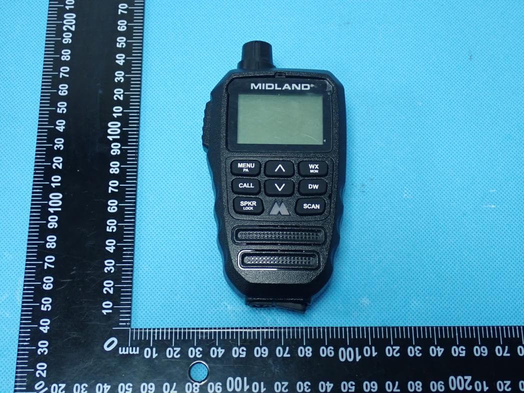
MMAMXMC95
Jun 10, 2026Wireless Bluetooth Microphone
Equipment Class
JAB - Part 15 Class B Digital Device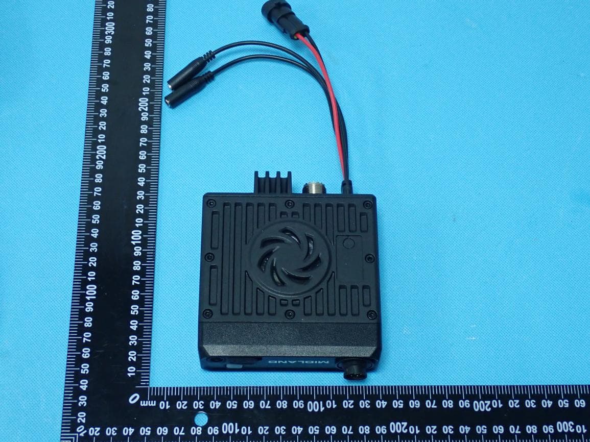
MMAMXT295
Jun 08, 2026GMRS Radio
Equipment Class
TNF - Licensed Non-Broadcast Transmitter Held to Face
MMACLIPTALK
Apr 27, 2026Transceiver
Equipment Class
DTS - Digital Transmission System
MMABR200S
Jan 13, 2026BUSINESS BAND TWO-WAY RADIO
Equipment Class
TNF - Licensed Non-Broadcast Transmitter Held to Face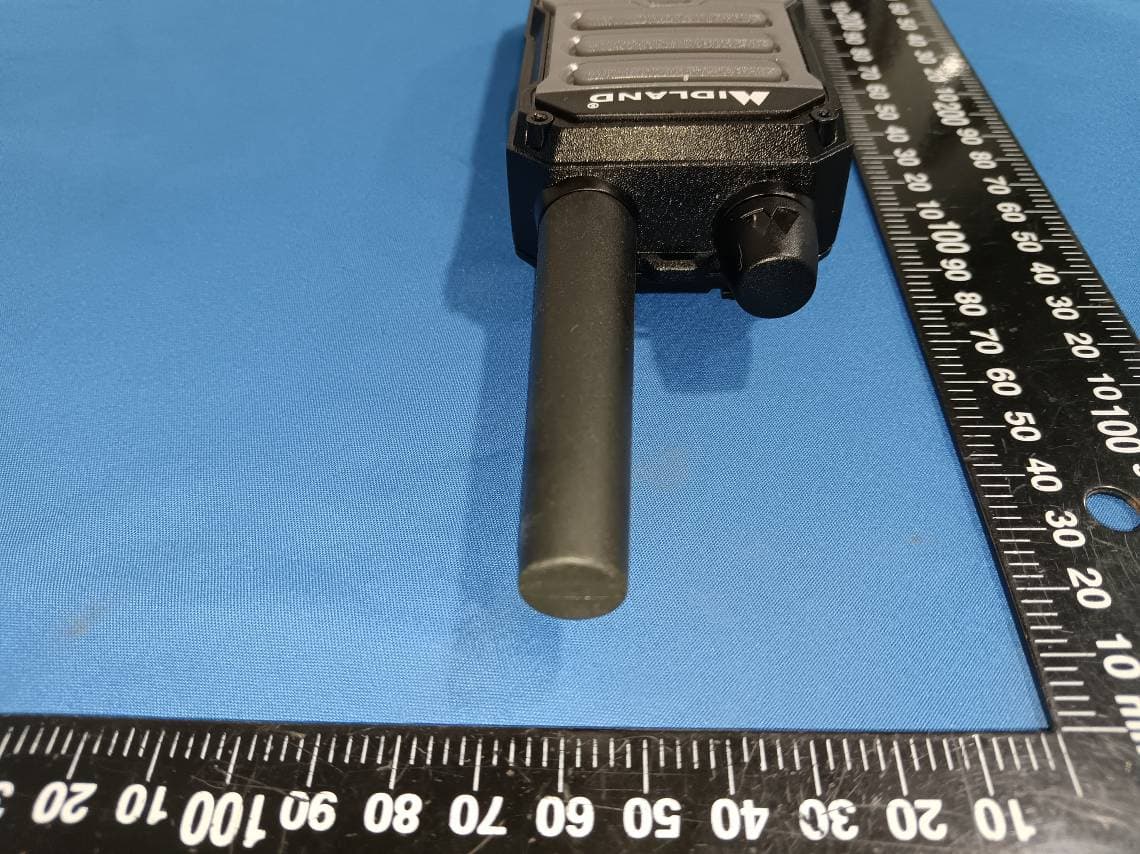
MMAGXT67
Oct 29, 2023GMRS RADIO
Equipment Class
TNF - Licensed Non-Broadcast Transmitter Held to Face