MMARG2Marine Transceiver
Midland Radio Corporation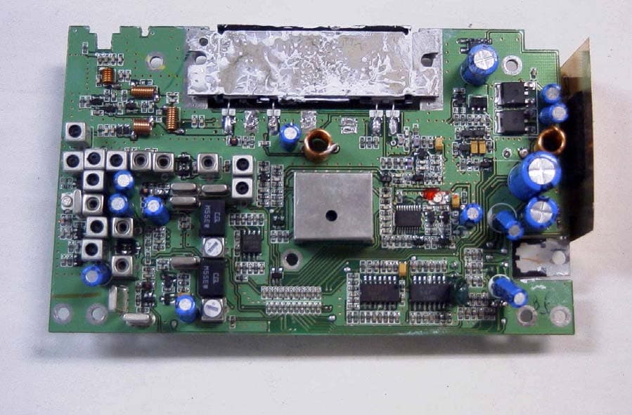
Click to zoom
Application Details
- Equipment Class
- TNB - Licensed Non-Broadcast Station Transmitter
- Date of Grant
- Dec 13, 2004
- Application Purpose
- Original Equipment
- Date of Application
- Dec 13, 2004
- Equipment Note
- Marine Transceiver
- Frequency Range
- 156.02500000 - 157.42500000
- Company
- Midland Radio Corporation
- Country
- United States
Documents & Files
Document Text
Text extracted from the exhibit documents filed with the FCC. Open a document above to read the original.
Users Manual
1 ENGLISH INDEX 1 ABOVE ALL... SAFETY! ..........................................................................................................3 1.1 Symbols used ................................................................................................................3 1.2 Warnings ........................................................................................................................3 1.2.a General ................................................................................................................3 1.2.b Radiofrequency/installation .................................................................................3 1.2.c Automatic Transmitter Identification System (ATIS) ...........................................3 1.2.d Environmental ......................................................................................................4 1.3 ETSI Information ............................................................................................................4 1.4 Registration of your Marine Transceiver ......................................................................4 1.5 Assistance .....................................................................................................................4 1.6 Manual Notes ................................................................................................................4 2 INTRODUCTION .....................................................................................................................5 2.1 Generalities ....................................................................................................................5 3 DESCRIPTION OF CONTROLS AND CONNECTORS .........................................................6 3.1 Front panel ....................................................................................................................6 3.2 Back panel (connections) ..............................................................................................7 3.3 Microphone ...................................................................................................................8 4 INSTALLATION .......................................................................................................................9 4.1 Contents of package .....................................................................................................9 4.2 Location for the transceiver .........................................................................................10 4.3 Mounting of transceiver ...............................................................................................10 4.4 Adjustment of angle ....................................................................................................11 4.5 Installation of the antenna/electromagnetic exposure ................................................11 4.6 Mounting of Microphone .............................................................................................12 4.7 Connections ................................................................................................................12 4.7.a Power Supply ....................................................................................................13 4.7.b GPS device ........................................................................................................13 4.7.c Antenna .............................................................................................................13 5 BASIC OPERATION ..............................................................................................................13 5.1 Turning NEPTUNE on/off .............................................................................................13 5.2 Volume regulation ........................................................................................................13 5.3 Squelch Regulation .....................................................................................................13 5.4 Selecting an operating channel ...................................................................................14 5.4.a With alphanumerical keypad .............................................................................14 5.4.b Using the microphone buttons (UP or DOWN) ..................................................14 5.5 Transmission and reception .........................................................................................14 5.6 Selecting high and low transmission power ................................................................14 5.7 Instant recall of channel 16 .........................................................................................15 5.8 Display lighting ............................................................................................................15 6 SCANNING FUNCTIONS .....................................................................................................16 6.1 Channel scanning ........................................................................................................16 6.2 Dual Watch and Triple Watch ......................................................................................16 6.3 Activation of Dual Watch/Triple ...................................................................................17 6.4 Memory channels (MEM mode) ...................................................................................18 6.4.a Memory scanning (SCAN MEMORY) ...............................................................18 6.4.b Reception/Transmission during SCAN MEMORY .............................................18 6.4.c To delete/To jump a pre-selected channel in memory ......................................18 2 ENGLISH 7 USE WITH GPS .....................................................................................................................19 7.1 Function ................................................................…
Text truncated - open the document above for the full version.
ID Label/Location Info
MODEL: REGATTA II VHF-FM MARINE TRANSCEIVER OPERATING VOLTAGE 13.8 VDC. FCC ID: MMARG2 SN MADE IN CHINA
Operational Description
THEORY OF OPERATION This PLL-controlled VHF marine DSC base station radio provides an accurate and stable multi-channel operation. Transmitter Receiver Local oscillator PLL(phase lock loop) circuit Memory backup DSC feature ATIS function Large LCD GPS message Transmitter The audio is picked up from the internal MIC. The audio signal is then amplified by audio amplifier, two of the quad operational amplifiers, U4 NJM3403, and filtered by low pass filter, two of the quad operational amplifiers, U5 NJM2904 .The audio level is adjusted by VR2 to obtain a suitable RF frequency deviation that then modulates the carrier of VCO, through varicap(VD1) The modulated signal output from the VCO is pre-amplified by Q303, Q304 and IC1. When the supply voltage is 12V, this signal will be amplified up to 1W or 25W. This signal is filtered by low-pass filter circuit that consists of L1, L3, L4, L5, C1, C2, C4, C5, C6, C7, C8 and C9,C10,C11. These low pass filters are necessary to suppress the second and the third harmonics. The filtered signal is then fed into the antenna input and radiated out. It is also fed into another path consisting of C330, C331, D301, D302 for sampling, and is converted into a direct current voltage for the automatic power control (APC) circuit Q307,Q306,Q305 whose collector current is used to maintain the output power stability. When the unit is transmitting, the channel control voltage is added to the TX VCO varicap VD2. The capacitance of VD1 is varied following the audio signal, thus the carrier is modulated to form the modulated signal. Receiver The receiver uses a double frequency super-heterodyne circuit. The first immediate frequency (IF) is 21.4MHz and the second is 455KHz. The RF signal is received by the antenna, and passes through a low-pass filter network L1, L3, L4, C1, C2, C4, C5, C7, C8, C10, C11 to filter out the unwanted signals. The received RF signal then passes through a high RF transformer T1 and is amplified ty RF amplifier Q1, T2, T3, T4, C19, C20, C23 form the band pass filter. The RF signal then is mixed with the local oscillation frequency by the diode loop mixer that consists of D2, D3, T5 and T6. The first IF(immediate frequency) of 21.4MHz is produced. This IF passes through a pair of crystal filter F1,F2 to further filter out the other unwanted signals. The first IF then is amplified by Q2 and the IF amplifier U1(S1T3361). U1 is an integrated FM IF demodulation circuit which consists of a local oscillator, a demodulator, a second mixer, squelch control circuit, and RF amplifier. the 21.4MHz IF then is mixed here with signal of the second local oscillator and converted into 2 nd immediate frequency (IF) 455KHz. The 2 nd IF passes through a ceramic filter F3 to filter out the residue unwanted signal, at pin 5 of IC4 (S1T3361)this final IF signal is output and the audio signal is output at pin 9 of IC4(S1T3361). The audio signal is amplified by U7B and passes through a volume control VR1, the amplified audio is then fed into de-emphasis circuit Q4 and finally amplified by audio amplifier U6(TDA2003) and heard from the speaker. The squelch control is also controlled by U1(S1T3361). The audio signal passes through the low pass filter R16, C46 and U1(S1T3361) internal squelch control R11, R12, C33, C34 and R13 that form as a squelch amplifier to produce a squelch signal (RF noise). This signal is amplified ty Q5 and regulated by D7 to produce a direct current voltage as a control voltage. The control voltage then is input to pin12 of U1(S1T3361). Pin13 of IC4 sends the digital squelch control signal to the MCU to mute the audio speaker path and to indicate the RX status through LCD. R40 and VR2 form a variable resistor, which correspond to the squelch level. Local oscillator PLL (phase lock loop) circuit The receiver and transmitter both share the same PLL (phase lock loop) circuitry to produce the carrier or the receiving frequency. The local oscillator consists of a phase lock loop(PLL) U3(LMX1511) Q401, Q402, Q502, Q503, and Q501. When Q501 is switched to saturation, the VCO will produce receiver local oscillator frequency. The fundamental frequency is determined by Y2(12.8MHz) and as the PLL reference oscillator. This signal is frequency-divided by U3 and a 12.5KHz signal is produced. When the VCO frequency applied to U3 pin10 and frequency-divided by U3 produces a frequency comparable to 12.5KHz, PLL will control the VCO. When these two frequencies are matched, a constant control voltage is output from PLL to lock VCO in desired frequency. Otherwise the PLL will also output an unlock indication to MCU to indicate that the PLL is in the frequency unlock state. Memory backup U2 is an EEPROM S524A60X51 , which acts as a memory backup for the working channel code and the system parameters. Every time when the unit is switched on, the MCU will reset the system, clear the RAM, and recall the memory from the EEPROM to refresh the RAM in MCU U1. DSC feature DSC is encoded by MCU U1, the passes through R18-R23 to produce D/A conversion and U4A low pass filter forms FSK signal. The FSK signal is amplified by U4C, U4B and filtered by U5A and U5B to modulate VCO frequency, thus the DSC signal is transmitted. The DSC signal is received and demodulated on the second receiver board. The demodulated signal is sent into main receiver U2 pin13, the signal from U2 pin 14 passes through U7D high-pass filter and U7C low-pass filter to get FSK signal and filter out residual unwanted signals. This FSK signal is decoded by U4. The DSC is restored and processed by MCU U1 with RX data from U4 pin7. Large LCD All message through series bus from MCU to display driver U6 will be displayed through a 1”x1.5” LCD in 4x12 characters dot matrix. GPS message External GPS message is input to MCU through phototransistor U10 TLP120. LCD will display the machine current location and time message in idle state.
Parts List/Tune Up Info
Model: Marine Transceiver B.O.M No. Customer: Standard Rev : S0 ELECTRONIC ENGINEER: HAM YIN CHECKED BY: Product: Issue Date : 31-MAR-04 MECHANICAL ENGINEER: Tony.Du APPROVED BY: Standard: ITEM P/N / DWG No. TYPE REFERENCE A PP'D MF G QTY HK$ VENDOR CODE REQ'DQTY ISSUE QTY FOLLOW QTY CH 1-1 311-6000003-2B1 Main PCB For Marine Transceiver ,137x83,FR4, T=1.6mm,D/S,T/P,REV:1 MAIN BOARD 1 1-2 305-S1T3361-200 IC,S1T3361D01-S0T0 'Samsung' 16SOP U1 U2 2 1-3 305-35H1516-100 IC,RF Power Module,RA35H1516M, Mitsubishi U11 1 1-4 305-JM2211M-100 IC, NJM2211M, DMP14, JRC U4 1 1-5 305-M3403AM-100 IC, NJM3403AM. SOP-14,JRC U7 1 1-6 305-JM78M08-100 IC, NJM78M08DLIA,TO-252, JRC U8 1 1-7 305-JM78M05-100 IC, NJM78M05DLIA,TO-252, JRC U9 1 1-8 305-LMX1511-100 IC, LMX1511TM, SSOP-20, National Semiconductor U3 1 CH 1-9 305-LTV354T-100 IC, OPTO, LTV-354T, LITEON U10 1 1-10 305-TDA2003-100 IC, TDA2003, SIG U6 1 1-11 305-JM2904M-100 IC, NJM2904M DMP8, JRC U5 1 1-12 303-6352LT1-100 UHF mixer Diode, MMBD352LT1,SMT, ON D2 D3 D201 D202 4 1-13 303-2KDS181-100 Switch Diode, KDS181, SMT, KEC D6 D15 D305 D401 D403 5 1-14 303-21SS314-100 VHF Band Switch Diode, 1SS314,Toshiba D1 D1A 2 1-15 303-2KDS184-100 Switch Diode, KDS184, SMT, KEC D303 1 1-16 303-2KDS226-100 Switch Diode, KDS226, SMT, KEC D7 D205 D402 3 1-17 303-21SS268-100 VHF Band Switch Diode, 1SS268, SMT,Toshiba D9 1 1-18 303-40BB133-100 VHF Variable Cap Diode, BB133 Philips VD1, VD2 2 1-19 303-1GW4007-100 Rectifier Diode,1A GW4007 SMT 'DC' D405 D406 2 1-20 303-6301LT1-100 VHF Detector Diode, MMBD301LT1, SMT,ON D301 D302 2 1-21 304-2SK302G-053 FET,Transistor, 2SK302G , SOT-23,Toshiba Q1 Q201 Q502 3 1-22 304-TC9018S-H01 Transistor, KTC9018S-H, SOT-23, EBC, KEC Q2 Q202 Q203 Q204 Q303 5 1-23 304-SC1623L-604 Transistor,NPN,2SC1623-L6,SOT-23,'NEC' Q4 Q5 Q205 Q306 Q402 5 1-24 304-3356R24-0A4 Transistor,NPN,2SC3356R24,SOT-23 'NEC' Q304 Q501 Q503 3 1-25 304-2SC4226-004 Transistor,NPN, 2SC4226, 'NEC' Q302 1 1-26 304-KTA1001-041 Transistor, PNP, KTA1001, SOT89, KEC Q403 1 1-27 304-2SA812M-604 Transistor,PNP,2SA812-M6,SOT-23,'NEC' Q305 Q307 Q401 Q404 4 1-28 304-KRC641T-0A1 Composite Transistor, KRC641. SOT-23.KEC Q406 1 1-29 304-KRA521T-0A1 Composite Transistor, KRA521T. SOT-23.KEC Q405 1 1-30 300-0500001-003 Chip Res,0603, 0 Ohm,1/16W,+/-5%,Tape Pack R3 R58 R201 3 1-31 300-0705081-033 Chip Res, 1206, 0.5 Ohm, 1/4W, +/-5%, Tape R52 R53 2 1-32 300-0502291-003 Chip Res, 0603,2.2 Ohm,1/16W,+/-5% Tape Pack R42 R44 2 1-33 300-0504791-003 Chip Res, 0603,4.7 Ohm,1/16W,+/-5% Tape Pack R59 1 1-34 300-0505691-003 Chip Res, 0603, 5.6 Ohm,1/16W,+/-5% Tape Pack R412 1 CH 1-35 300-0501001-003 Chip Res,0603,10 Ohm,1/16W,+/-5%,Tape Pack R10A R212 C24A 3 1-36 300-0502201-003 Chip Res, 0603,22 Ohm,1/16W,+/-5% Tape Pack R51 R312 R316 3 1-37 300-0503901-003 Chip Res, 0603,39 Ohm,1/16W,+/-5% Tape Pack R41 2 1-38 300-0504701-003 Chi p Res 0603 47 Ohm 1/16W +/-5% Ta p e R8 R15 R206 R503 R509 R510 6 WINKLER INDUSTRIAL CO., LTD. #1 ELECTRONICS COMPONENTS (1) RECEIVER SECTION 1 18 Model: Marine Transceiver B.O.M No. Customer: Standard Rev : S0 ELECTRONIC ENGINEER: HAM YIN CHECKED BY: Product: Issue Date : 31-MAR-04 MECHANICAL ENGINEER: Tony.Du APPROVED BY: Standard: WINKLER INDUSTRIAL CO., LTD. AD D 1-39 300-0506801-003 Chip Res 0603 68 Ohm 1/16W +/-5% Tape R319 1 1-40 300-0501011-003 Chip Res, 0603,100 Ohm,1/16W,+/-5% Tape Pack R50 R204 R224 R228 R5 R217 R313 R209 R331 R408 R409 R410 R413 R502 R508 R332 R335 17 1-41 300-0501811-003 Chip Res, 0603,180 Ohm,1/16W,+/-5% Tape Pack R219 1 1-42 300-0502211-003 Chip Res, 0603,220 Ohm,1/16W,+/-5% Tape Pack R43 R329 R330 R404 R49 R205 R227 7 1-43 300-0503911-003 Chip Res, 0603, 390 Ohm, 1/16W, +/-5% Tape R320 R402 2 1-44 300-0505611-003 Chip Res, 0603, 560 Ohm,1/16W,+/-5% Tape Pack R417 1 1-45 300-0506811-003 Chip Res, 0603, 680 Ohm, 1/16W, +/-5% Tape R315 1 1-46 300-0501021-003 Chip Res, 0603, 1K, 1/16W,+/-5% Tape Pack R48 R411 R504 3 1-47 300-0501221-003 Chip Res, 0603, 1.2K,1/16W,+/-5% Tape Pack R6 R207 R244 3 1-48 300-0501521-003 Chip Res, 0603, 1.5K,1/16W,+/-5% Tape Pack R37 1 1-49 300-0501821-003 Chip Res, 0603, 1.8K,1/16W,+/-5%,Tape Pack R12 1 CH 1-50 300-0502221-003 Chip Res, 0603, 2.2K,1/16W,+/-5% Tape Pack R20 R215 R311 R403 R35 R57 R415 R416 R420 9 1-51 300-0503321-003 Chip Res, 0603, 3.3K,1/16W,+/-5% Tape Pack R213 R314 R401 3 1-52 300-0503921-003 Chip Res, 0603, 3.9K,1/16W,+/-5% Tape Pack R214 1 1-53 300-0504721-003 Chip Res, 0603,4.7K,1/16W,+/-5% Tape Pack R2 R4 R45 R46 R47 R54 R56 R222 R309 R333 R334 R419 R505 13 1-54 300-0506821-003 Chip Res, 0603, 6.8K,1/16W,+/-5%,Tape Pack R11 R225 R220 R308 4 1-55 300-0501031-003 Chip Res, 0603, 10K,1/16W,+/-5% Tape Pack R9 R33 R36 R100 R210 R229 R232 R234 R239 R321 R324 R327 R328 R405 R406 R407 R506 17 AD D 1-56 300-0501231-003 Chip Res, 0603, 12K,1/16W,+/-5% Tape Pack R19A 1 1-57 300-0501531-003 Chip Res, 0603, 15K,1/16W,+/-5% Tape Pack R226 R310 R230 R301 4 1-58 300-0501831-003 Chip Res, 0603, 18K,1/16W,+/-5% Tape Pack R14 R221 2 CH 1-59 300-9620021-012 Chip Res(High Precision),0603,20K,1/10W,+/-2%,Tape Pack R245 1 1-60 300-0502231-003 Chip Res, 0603, 22K,1/16W,+/-5% Tape Pack R16 R326 R237 R238 R38 R305 R337 7 1-61 300-0503331-003 Chip Res, 0603, 33K,1/16W,+/-5% Tape Pack R10 R211 R236 R303 4 1-62 300-0504731-003 Chip Res, 0603, 47K,1/16W,+/-5% Tape Pack R1 R24 R25 R40 R243 R302 R304 R414 R501 10 1-63 300-0506831-003 Chip Res,0603,68K, 1/16W,+/-5%,Tape Pack R18 R307 R336 3 1-64 300-0501041-003 Chip Res, 0603, 100K,1/16W,+/-5% Tape Pack R223 R235 R242 R246 R507 R306 6 AD D 1-651-66 300-0501541-003 Chip Res, 0603, 150K,1/16W,+/-5% Tape Pack R216 R34 2 1-67 300-0502241-003 Chip Res, 0603, 220K,1/16W,+/-5% Tape Pack R7 R13 R39 R208 R231R233 R325 7 1-68 300-0503341-003 Chip Res, 0603, 330K,1/16W,+/-5% Tape Pack R218 1 1-69 300-0503941-003 Chip Res, 0603, 390K,1/16W,+/-5% Tape Pack R55 1 2 18 Model: Marine Transceiver B.O.M No. Customer: Standard Rev : S0 ELECTRONIC ENGINEER: HAM YIN CH…
Text truncated - open the document above for the full version.
Parts List/Tune Up Info
eAdjustm StepItemAdjustment 1 TX FrequencyVC1 2 TX PowerVR1,VR3 3TX Dev.VR2 4RX T1 T16 T2 T3 T4 T5 T7 T8 T9 5 RX 70CHT13 T15 T17 T18 T10 ent Procedure Procedure Adjust VC1 to obtain demanded TX carrier frequency. Separately adjust VR1 and VR3 to obtain demanded low and high TX power. Check MIC modulation sensitivity, which should be 2.5~20mV. Inject an audio frequency(AF) -20dBm. Adjust VR3 to obtain maximum TX deviation 5kHz. Check RX sensitivity if it is poor.Adjust T1,T16,T2,T3,T4,T5,T7,T8,and T9 to obtain best band sensitivity. Check RX 70CH sensitivity if it is poor.Adjust T13,T15,T17,T18,and T10 to obtain best band sensitivity.
Test Report
TIMCO ENGINEERING INC. 849 NW State Road 45 Newberry, Florida 32669 http://www.timcoengr.com 888.472.2424 F 352.472.2030 email: [email protected] APPLICANT: MIDLAND RADIO CORPORATION FCC ID: MMARG2 REPORT #: M\MidlandRadio_MMA\1768AUT4\1768AUT4\1768AUT4TestReport.doc COVER PAGE Test Report Product Name: MARINE TRANSCEIVER FCC ID: MMARG2 Applicant: MIDLAND RADIO CORPORATION 1120 CLAY STREET NORTH KANSAS CITY MO. 64116 Date Receipt: OCTOBER 26, 2004 Date Tested: NOVEMBER 15, 2004 TIMCO ENGINEERING INC. 849 NW State Road 45 Newberry, Florida 32669 http://www.timcoengr.com 888.472.2424 F 352.472.2030 email: [email protected] APPLICANT: MIDLAND RADIO CORPORATION FCC ID: MMARG2 REPORT #: M\MidlandRadio_MMA\1768AUT4\1768AUT4\1768AUT4TestReport.doc TABLE OF CONTENTS APPLICANT: MIDLAND RADIO CORPORATION FCC ID: MMARG2 TABLE OF CONTENTS LIST TEST REPORT: PAGE 1............GENERAL INFORMATION & TECHNICAL DESCRIPTION PAGE 2............TECHNICAL DESCRIPTION CONTINUED RF POWER OUTPUT PAGE 3............TECHNICAL DATA PAGE 4............VOICE MODULATION CHARACTERISITICS AUDIO FREQUENCY RESPONSE PAGE 5............AUDIO LOW PASS FILTER PAGE 6............MODULATION LIMITING PAGE 7............OCCUPIED BANDWIDTH PAGE 8-9..........OCCUPIED BANDWIDTH PLOTS PAGE 10...........SPURIOUS EMISSIONS AT ANTENNA TERMINALS PAGE 11...........METHOD OF MEASURING CONDUCTED SPURIOUS EMISS PAGE 12-13........FIELD STRENGTH OF SPURIOUS EMISSIONS PAGE 14...........METHOD OF MEASURING RADIATED SPURIOUS EMISSIONS PAGE 15...........FREQUENCY STABILITY PAGE 16...........MPE CALCULATION PAGE 17-22........LIST OF TEST EQUIPMENT EXHIBITS INCLUDING: BLOCK DIAGRAM SCHEMATIC PARTS LIST USERS MANUAL LABEL SAMPLE LABEL LOCATION EXTERNAL PHOTOGRAPHS INTERNAL PHOTOGRAPHS OPERATIONAL DESCRIPTION TUNING PROCEDURE TEST SET UP PHOTOGRAPHS TIMCO ENGINEERING INC. 849 NW State Road 45 Newberry, Florida 32669 http://www.timcoengr.com 888.472.2424 F 352.472.2030 email: [email protected] APPLICANT: MIDLAND RADIO CORPORATION FCC ID: MMARG2 REPORT #: M\MidlandRadio_MMA\1768AUT4\1768AUT4\1768AUT4TestReport.doc Page 1 of 21 GENERAL_INFORMATION 2.1033(c) MIDLAND RADIO CORPORATION will sell the FCC ID: MMARG2 VHF Marine transmitter in quantity, for use under FCC RULES PART 80. 2.1033(c) TECHNICAL_DESCRIPTION (4) Type of Emission: 16K0G3E/16K0F3E Bn = 2M + 2DK M = 3000 D = 4.6KHz (Peak Deviation) K = 1 Bn = 2(3.0K) + 2(4.6K)(1) = 6.0K + 10.0 = 16.0K 80.205 (a) ALLOWED AUTHORIZED BANDWIDTH = 20.00KHz. (5) Type of Emission: 16K0G3E/16K0F3E Bn = 2M + 2DK M = 3000 D = 4.6KHz (Peak Deviation) K = 1 Bn = 2(3.0K) + 2(4.6K)(1) = 6.0K + 10.0 = 16.0K FOR DSC ALLOWED AUTHORIZED BANDWIDTH = 20.00KHz. 2.1033(c)(6) Frequency Range: 156.025 – 157.425 MHz 2.1033(c)(7) Power Range and Controls: There is a user Power switch for High/Low Power. Maximum Output Power Rating: High 25 Watts, Low 1 Watt into a 50 ohm resistive load. 2.1033(c)(8) DC Voltages and Current into Final Amplifier: POWER INPUT (CHANNEL 1) FINAL AMPLIFIER ONLY High Low Vce = 12 VDC Vce = 12 VDC Ice = 4.38 A Ice = 0.88 A Pin = 52.56 Watts Pin = 10.56 Watts POWER INPUT (CHANNEL 88) FINAL AMPLIFIER ONLY High Low Vce = 12 VDC Vce = 12 VDC Ice = 4.32 A Ice = 0.87 A Pin = 51.84 Watts Pin = 10.44 Watts TIMCO ENGINEERING INC. 849 NW State Road 45 Newberry, Florida 32669 http://www.timcoengr.com 888.472.2424 F 352.472.2030 email: [email protected] APPLICANT: MIDLAND RADIO CORPORATION FCC ID: MMARG2 REPORT #: M\MidlandRadio_MMA\1768AUT4\1768AUT4\1768AUT4TestReport.doc Page 2 of 21 Function of each electron tube or semiconductor device or other active circuit device is included in the parts list exhibit. 2.1033(c)(9) Complete Circuit Diagrams: The circuit diagrams and block diagrams are included. 2.1033(c)(10) Instruction book. The instruction manual is included. 2.1033(c)(11) Tune-up procedure. The tune-up procedure is included. Description of all circuitry and devices provided for determining and stabilizing frequency is included in the circuit description 2.1033(c)(11) Digital modulation. This unit does NOT use digital modulation. The data required by 2.1046 through 2.1055 is submitted below. 2.1046(a) RF_power_output. 80.215 (e)(1) RF power is measured by connecting a 50 ohm, re- sistive wattmeter to the RF output connector. With a nominal battery voltage, and the transmitter properly adjusted the RF output measures: OUTPUT POWER: HIGH: 25 W CONDUCTED LOW: 1 W CONDUCTED 80.911 (d)(5) For primary supply voltages, measured in accordance with the procedures in this paragraph, greater than 11.5 volts, but less than 12.6 volts, the required transmitter output power shall be equal or greater than the value calculated below P = 4.375(v) – 35.313 (For 12V this equals 17.2W) METHOD OF MEASURING RF POWER OUTPUT Transmitter 50 ohm under test Resistive Wattmeter Power Supply TIMCO ENGINEERING INC. 849 NW State Road 45 Newberry, Florida 32669 http://www.timcoengr.com 888.472.2424 F 352.472.2030 email: [email protected] APPLICANT: MIDLAND RADIO CORPORATION FCC ID: MMARG2 REPORT #: M\MidlandRadio_MMA\1768AUT4\1768AUT4\1768AUT4TestReport.doc Page 3 of 21 TECHNICAL DATA: 80.203 (b) External Controls: The transmitter is capable of changing frequency between 156.05 – 157.425 MHz by external control. The available channels are shown in the User Manual description Channel List. These channels are preprogrammed by the manufacturer and change of frequency is inaccessible to the station operator. 80.203 (c) Five minutes continuous transmission test. The antenna was connected to a dummy load and the radio was locked in a transmit PTT mode. An external timer digital clock was used to observe the duration of the un-modulated transmission. The transmitter turned off and the radio went to receive mode at 4 minutes, 58 seconds as displayed by the external digital clock. 80.203 (n) This radio complies with the requirement for DSC capability in the 156 – 162 MHz band and in accordance with 80.225. 80.873; 80.956 Transmitter G3E emission capabilit…
Text truncated - open the document above for the full version.
Contact Information
Applicant
Butch Rittmann(Director of Operations)
Test Firm
Timco Engineering, Inc.S Sanders
Technical Specifications
| # | Rule Parts | Frequency Range | Power Output | Emission | Tolerance |
|---|---|---|---|---|---|
| 4 | 8 | 156.025 MHz - 157.425 MHz | 1 W | 16K0G3E | 10 ppm |
Other Applications from Midland Radio Corporation
MMAMXMC95
Jun 10, 2026Wireless Bluetooth Microphone
Equipment Class
JAB - Part 15 Class B Digital Device
MMAMXT295
Jun 08, 2026GMRS Radio
Equipment Class
TNF - Licensed Non-Broadcast Transmitter Held to Face
MMACLIPTALK
Apr 27, 2026Transceiver
Equipment Class
DTS - Digital Transmission System
MMABR200S
Jan 13, 2026BUSINESS BAND TWO-WAY RADIO
Equipment Class
TNF - Licensed Non-Broadcast Transmitter Held to Face
MMAGXT67
Oct 29, 2023GMRS RADIO
Equipment Class
TNF - Licensed Non-Broadcast Transmitter Held to Face