MMASD174UHF TRANSCEIVER TRANSMITTER PORTION
Midland Radio Corporation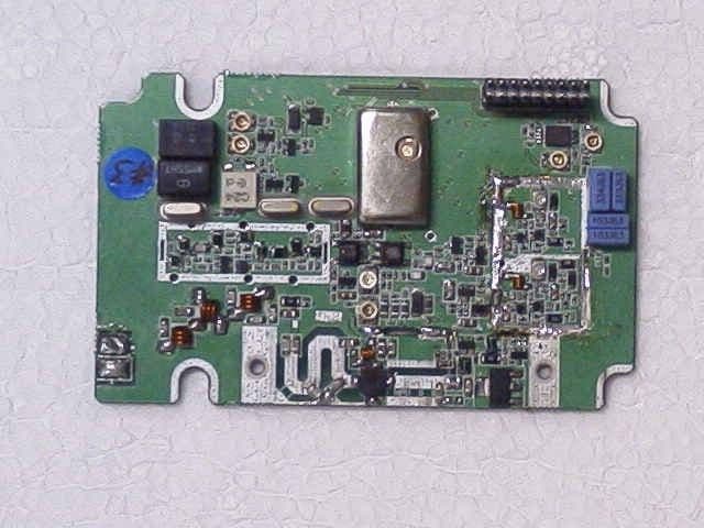
Click to zoom
Application Details
- Equipment Class
- TNB - Licensed Non-Broadcast Station Transmitter
- Date of Grant
- Jan 04, 2004
- Application Purpose
- Original Equipment
- Date of Application
- Jan 04, 2004
- Equipment Note
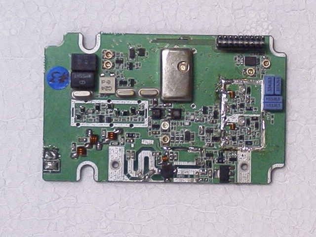
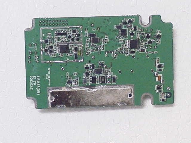
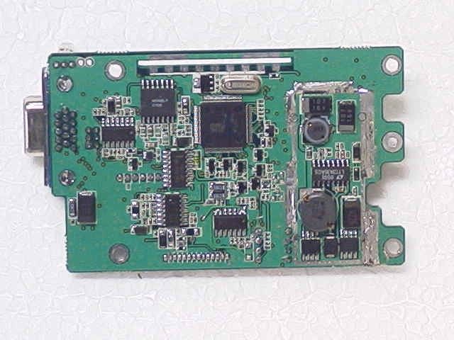
- UHF TRANSCEIVER TRANSMITTER PORTION
- Frequency Range
- 450.00000000 - 490.00000000
- Company
- Midland Radio Corporation
- Country
- United States
Documents & Files
Document Text
Text extracted from the exhibit documents filed with the FCC. Open a document above to read the original.
Users Manual
SD-174 Data Radio User Instruction Manual 2 FCC RF Exposure Compliance Requirements The Federal Communications Commission (FCC), with its action in General Docket 93-62, November 7, 1997, has adopted a safety standard for human exposure to Radio Frequency (RF) electromagnetic energy emitted by FCC regulated equipment. Maxon subscribes to the same safety standard for the use of its products. Proper operation of this radio will result in user exposure far below the Occupational Safety and Health Act (OSHA) and Federal Communications Commission limits. Power listed is conducted. This device must not exceed a maximum transmitting duty factor of 50%. The antenna(s) used for this transmitter must be installed to provide a separation distance of at least 49cm (19.29 inches) from all persons, must not be co-located or operating in conjunction with any other antenna or transmitter, and must not exceed a gain of 7 dBc. Failure to observe these restrictions will result in exceeding the FCC RF exposure limits. About your SD-170 Series Data Radio The SD-170 Series of RF Link Modules utilize the latest technology in their designs and manufacturing. SD-170 models are Phase Lock Loop Synthesizer (PLL) / microprocessor controlled and offer two (2) watts of power with 16-channel capability. Multiple functions including 1200 to 9600 baud rates, AC and/or DC audio coupling, GMSK, FFSK and FSK modulation are standard in these fully programmable RF Link Module units. Programmable sub-audio squelch system (CTCSS & DCS) and two-tone squelch system are added to the signal level detect squelch system (RSSI). GPS Data handling is provided to interface and control an internal GPS receiver. To assure satisfaction from the radio, we urge you to thoroughly read the operation and function information in this manual before operating your SD-174. Applications of some of the functions described in this manual are determined by the system you use. Your dealer will program your radio so that you have the greatest number of functions possible relative to your needs. Should you have questions regarding the operation of the radio, please consult your Dealer. 3 Specifications GENERAL Equipment Type ............................................................... Data radio Performance Specifications................................................TIA / EIA-603 & AS-4295 Band .............................................................................. UHF Channel Spacings ............................................................ 25 kHz, 12.5 kHz programmable RF Output Power ............................................................ 5 watt / 1 watt programmable Modulation Type ............................................................ F2D, F3E Intermediate Frequency ................................................... 45.1 MHz & 455 kHz Number of Channels ......................................................... 16 Frequency Source ............................................................ Synthesizer Operation Rating ............................................................ Intermittent 90 : 5 : 5 (Standby: RX: TX) Power Supply .................................................................. Ext. Power Supply(12 VDC Nominal) 9V - 18.0V DC EXTREME Temperature Range Storage ........................................................................... from - 40°C to + 80°C Operating ........................................................................ from - 30°C to + 60°C Current Consumption Standby (Muted) ............................................................... < 65 mA Transmit 2 Watt RF power ................................................ < 1.0 A Frequency Bands: RX TX UHF : U2 450.000 - 490.000 MHz 450.000 - 490.000 MHz Lock Time ........................................................................ < 10 mS TX to RX attack time ......................................................... < 20 mS (No Power Saving) RX to TX attack time ......................................................... < 20 mS Dimensions..................................................................... (32 mm)H x (58 mm)W x (125 mm)D Weight ........................................................................... 253 grams 4 TRANSMITTER Specification Carrier Power: .................................................................. Nom. Max. Min. High ..................................................................5W < 6W > 4.5W Low ..................................................................1W < 1.5W > 0.8W Sustained Transmission ................................................... Nominal conditions Time : 5 10 30 Sec. Power: >90% >85% >80% Frequency Error ............................................................... ±5.0 ppm Extreme condition for UHF Frequency Deviation: 25 kHz Channel Spacing................................................... Peak ±5.0, Min. ±3.8 12.5 kHz Channel Spacing................................................ Peak ±2.5, Min. ±1.9 Audio Frequency Response................................................ Within +1/-3dB of 6dB octave @ 300 Hz to 2.55 kHz for 12.5 kHz C.S. @ 300 Hz to 3.0 kHz for 25 kHz C.S. Adjacent Channel Power 25 kHz ........................................................................... < 70 dBc @ Nominal Condition < 65 dBc @ Extreme Condition 12.5 kHz ........................................................................ < 60 dBc @ Nominal Condition < 55 dBc @ Extreme Condition Conducted Spurious Emission .......................................... < -60 dBc Modulation Sensitivity ...................................................... 100mV RMS @ 60 % Peak Dev. Hum & Noise: 25 kHz Channel Spacing ................................................... > 40 dB (with no PSOPH) 12.5 kHz Channel Spacing ................................................ > 40 dB (with PSOPH) Modulation Symmetry ...................................................... < 10 % Peak Dev @ 1 kHz input f…
Text truncated - open the document above for the full version.
Operational Description
BRIEF CIRCUIT DESCRIPTION INTRODUCTION The VHF and UHF radios comprise of two PCBs (RF and digital PCB). These boards are connected by an 18 pin female and male connector. The digital board which controls the radio and data receiving and sending is interfaced with external data equipment through the 15 pin d-sub female (DB-15) connector. DIGITAL CIRCUITS The Digital circuit contains the CPU, the channel select switch, and associated digital circuits. TX-SIGNAL CIRCUIT There are two signal paths in the Tx-signal circuit. One is FSK data signal path and the other is the audio signal path. The FSK data signal from Pin 1 of DB-15 connector (CON401) goes through IC406-C. The signal is amplified by IC404-C and then its amplitude is limited by IC404-D. After that, this signal is filtered by an 8’th order low pass filter (IC405) in order to reduce the required transmission bandwidth. The first two stages of the 8’th order LPF consist of a Gaussian filter for the improvement of ramp function response and the last two stages use a Butterworth filter for attenuation. The output of the LPF is then fed to the RF board for TX modulation. Audio signal, from Pin 7 of DB-15 connector is fed into the 300Hz High pass filter(IC408) through the IC406-B and IC409. The HPF removes sub-audible voice products for application of Sub-audio(Tone) squelch system (CTCSS, DCS) and then the output from IC408 is fed into IC404-A&B with associated parts to form a mic amplifier and pre-emphasis circuit. After that, the pre-emphasized Tx-audio signal is inputted to the RF board for Tx modulation through the FSK data signal path. RX-SIGNAL CIRCUIT The Rx-signal circuit also has two signal paths. One is the data signal path and the other is the audio signal path. The Rx signal comes from the RF board, which is connected with pin 10 of CON405. Data signals are switched in IC406-D by a Busy signal which is activated when the radio receives a valid RF signal, and is filtered by IC416-A and then its amplitude level is adjusted (amplified) by IC416-B. The amplitude-adjusted signal goes to pin 2 of the DB-15 connector (CON401). Audio signals are inputted to the 300Hz High pass filter (IC408) to eliminate sub-audible voice products through IC409. The output of the HPF is switched by IC406-A and de-emphasized by resister R471 and C452. After that, its level is adjusted by RV401 and then that is amplified by IC412 (LM386 : Audio amplifier). The amplified signal goes to pin 9 of CON401 (DB-15). ANALOG SWITCH IC409 (MC14053B) is a digitally controlled analog switch which internally consists of three single pole, double throw switches. By placing a high (5V) or low (0V) on the control lines which consists of A, B and C. A controls the X ports, B controls the Y ports and C controls the Z ports. Example: A high on control A would connect X to X1. A low on control A would connect X to X0. HIGH PASS FILTER The 300Hz high pass filter is an 8-pole 1dB Chebeyshev active filter that comprises of IC410 and associated components. Received audio is passed to IC408 from Pin 4 of IC409 where sub-audible tones below 300Hz are removed. Tx (Mic) audio is also fed into IC408 via IC 409 (Pin 4) where sub-audible voice products below 300Hz are also removed. CTCSS/DCS DECODE CIRCUITS Discriminated audio from Pin 9 of IC6 is fed into IC411-B and associated parts which are the first 2 poles are part of a 6th order 250 Hz Chebeyshev low pass filter. The output from pin 1 (IC411-B) is fed into IC409 (Pin 2) and outputs to pin 15 (IC409). The signal is then fed to Pin 8 (IC410) which is a 6th order low pass Butterworth switched capacitor filter. The output from the Butterworth filter (Pin 3 of IC410) is then fed to the remaining second 4 poles part of the 6th order Chebeyshev filter, which consist of IC411- D and one of the two internal operational amplifiers of IC410 (MSNBLPS) along with associated components. Both the Chebeyshev and the Butterworth combines for a 4dB ripple low pass filter when programmed for 250 Hz. The output of IC411-D (Pin 14) is fed into the remaining internal operational amplifier of IC410 (MSNBLPS) which forms the squaring circuit for the signal decode. The signal is out from Pin 2 of IC411 (MSNBLPS) and fed into IC401 (MCU) where it is compared whether that is matched with preprogrammed data or not. If matched, valid data is decoded, shown by a green L.E.D. on the top panel of the radio, and audio is released through pin 9 of DB-15 Connector. If unmatched, the busy L.E.D. (Yellow) would be shown. CTCSS/DCS ENCODE CIRCUITS During TX encode, the tone squelch digital signal is produced as a 3-bit parallel word at Pins 33, 34, and 35 of the micro controller (IC401). The 3-bit digital signal is converted to an analog signal by resistors R481, 482 and 483. The analog signal is fed into Pin 1of IC409 and out on Pin 15 (IC409) and then fed into Pin 8 of IC410 (6th order Butterworth clock tuned low pass filter). The filtered encode output from Pin 3 (IC410) is fed to IC411-A and RV402 (sub-audible gain control), the output of IC411-A is then fed to the audio mixer circuit of the RF board. TWO TONE DECODE CIRCUITS Two tone uses frequency with audio. Discriminated audio from the RF board is inputted to the comparator (two tone decoder : IC403-B) which forms the squaring circuit for the decode signal. The signal is output from Pin 7 of IC403-B and fed into IC401 (MCU) where it is compared whether it is matched with preprogrammed data or not. If matched valid data is decoded, which is shown by a green L.E.D. on the top panel of the radio and audio is released through pin 9 of the DB-15 Connector. If unmatched, the busy L.E.D. (Yellow) is shown. RSSI DETECTOR From the RF board, the RSSI (Received Signal Strength Indicator) signal flows to Pin 31 of IC401(MCU) through R513. Micro controller unit (IC401) detects received signal level using the inner 8-bit ADC(Analog to Digital Converter). The output of ADC is compared with the programmed RSSI level. …
Text truncated - open the document above for the full version.
Parts List/Tune Up Info
1 Alignment method for SD-160 Series 1. Introduction There are many alignment points in SD-160 and some of them need critical alignment. Especially, ACC-516 (PCB Extender) isn’t useful for alignment in RF board is connected to BNC connector of bottom cover. So, we recommend the modification of ACC-516, flexible PCB extender, and use of RF cable which has BNC connector at the end, RF test cable, showed in Fig.2.1, 2.2. This document describes required preparation for alignment and its procedure. RV4 RV3 RV5 RV6 TCXO1 C208C308 RV1 RV2 TP1 RF BOARD RV402 RV401 SW401 DIGITAL BOARD CON407 RV403 SQ for N-BAND SQ for S-BAND Balence Deviation Tone Deviation Outpt Audio level Ref. level for Modem Power Figure 1.1. Alignment points of SD-164 2 2. Preparation 2.1. Required accessories for alignment a. Flexible PCB Extender - It’s modified from ACC-516. Figure 1.1. Flexible PCB Extender b. RF test cable – It consists of BNC connector and RG-178 RF cable. Figure 2.2. RF test cable 3 2.2. Preparation for alignment a. Solder end of RF test cable to PCB land for antenna cable of RF board Figure 2.2. Soldering RF test cable to RF board b. Connect RF board to Digital board with Flexible PCB extender. Figure 2.3. Connecting RF board to Digital board 4 3. Alignment procedure The SD-160 should require no special alignment, unless repairs are performed on the transceiver portion. Should repairs be necessary, use the "Test Equipment Diagram (refer to technical manual for SD-160)" and the Alignment Points Diagram (refer to Fig. 1.1)", in conjunction with the following procedures: ☞ An Flexible PCB Extender, which is modified fromACC-516, is required in order to separate the Digital and RF PCB’s to allow access to the alignment points. Installation instructions are provided with the Extender Assembly. 3.1. RECEIVER (1) RX VCO RX VCO is pre-tuned at factory and no more adjustment is required. To identify existence of defect of RX VCO, check the VCO Control voltage. 1. Set the unit to the highest receive frequency, 490MHz(UHF2) and check the VCO control voltage is under 10.0 Volts. If it’s over 10.0 Volts, adjust C308 of RX VCO to 10.0 Volts 2. Set the unit to the lowest receive frequency 450MHz(UHF2) and check that the VCO voltage is above 2.0 Volts. Adjust C308 to 2.0 Volts ※ Note: Use TP1 to measure the voltage. (2) AUDIO OUTPUT LEVEL Adjustment 1. Select a receiver channel that is programmed for Standard band (25kHz) operation. 2. Prepare standard test signal as follows. Set the RF signal generator to the receiver frequency. And then set the AF modulation signal to 1 kHz at 3kH deviation. Adjust the RF output level of the RF signal generator to –47dBm. 3. Apply a standard test signal to the receiver antenna terminals. 4. Adjust RV401 for the specific audio output level. 5 (3) LEVEL SHIFTER for Modem option Board (ACC-513, ACC-514) 1. Select a receiver channel which is programmed for Standard band (25kHz) operation. 2. After Preparing standard test signal for Standard band, apply that signal to the antenna terminals of receiver. 3. Adjust RV403 until the center voltage of demodulated signal (1KHz sine wave) of TP401 is 2.5 Volts. 4. Select a receiver channel which is programmed for Narrow band (12.5kHz) operation. 5. After Preparing standard test signal for Narrow band (only decrease deviation of AF modulation signal as 1.5K from standard test signal for Standard band), apply that signal to the antenna terminals of receiver. 6. Check the center voltage of demodulated signal of TP401 is 2.5 Volts. If different, Adjust RV403 until the center voltage is near 2.5 Volts for each band (25KHz / 12.5KHz). 3.2. TRANSMITTER Connect the unit to a Service Monitor with the power meter set to the 10 W scale (or autorange) (1) TCXO Set the channel selector to the mid-range frequency 470 MHz, adjust TCXO1 for a reading of 470MHz ±200Hz. (2) TX VCO TX VCO is pre-tuned at factory and no more adjustment is required To identify existence of defect of TX VCO, check the VCO Control voltage. 1. Set the unit to the highest transmit frequency, 490MHz(UHF2), key the transmitter and check the VCO control voltage is under 10.0 Volts. If it’s over 10.0 Volts, adjust C208 of TX VCO to 10.0 Volts. 2. Set the unit to the lowest transmit frequency 450 MHz(UHF2), key the transmitter and check that the VCO voltage is above 1.8 Volts. Adjust C208 to 1.8 Volts 6 ※Note: use TP1 to measure the voltage. (3) CTCSS, DCS & TX Deviation and Balance Adjustment 1. a. Set the unit to a mid-frequency range and a CTCSS of 67Hz. Push PTT and adjust RV402 for desired CTCSS tone deviation. b. Switch to a channel with the same frequency and CTCSS of 250.3Hz. Push PTT and adjust RV1 to desired CTCSS tone deviation, same as above step. c. Switch between the 67Hz channel and the 250.3Hz channel and adjust RV1 until the deviation is the same on both channels. It may be necessary to readjust RV402 to get the desired deviation. 2. Set the unit to a mid-frequency and input the TX data with 400 Hz standard audio level. 3. Increase the signal level to 20 dB from standard level. 4. Monitor the demodulated signal from service monitor. Adjust RV1 to make the monitored signal to be a balanced square wave. 5. Reduce input signal to the standard level and adjust RV2 for the standard deviation. (4) APC Adjust RV4 for RF transmission power. (2W, SD-161, SD-164) This is the most critical point of the transmitter alignment procedures. If you use ACC- 516 (PCB Extender Board) or Flexible PCB Extender, that has a voltage drop in transmission mode and so power drop occurs. That’s the reason that radio outputs higher power than assigned after assembly. To prevent over power output, follow below procedure. !! In case that ACC-516 (PCB Extender Board) is used for alignment : ① Set the power at the point of 1.25W. ② Assemble the radio and then check again RF transmission power is near 2.0W. !! In case that Flexible PCB Extender is used for alignment : ① Set the power at the point of 1.6W.…
Text truncated - open the document above for the full version.
Parts List/Tune Up Info
Part List of SD-174 1. COVER ASSEMBLY (Part No. : 577-74C-A) ------------------------------------------------------------------------------------------------------- PART-NO. NAME & DESCRIPTION Q'TY REFERENCE-NO ------------------------------------------------------------------------------------------------------- 421-406-4 CONNECTOR BNC BNC-RB-CRIMP-1781U 1 421-414-7 CONNECTOR SCW-12-2(R) SW-2334 1 612-036 (+)MACHINE SCREW(PH)2X6 ZN-PLAT 3 613-323 (+)MACHINE SCREW(BH)3X8 NI-PLAT 4 71A-061 COVER UPPER ALDC 12 1 71A-062 COVER BOTTOM ALDC 12 1 761-783-A HEAT SINK CUP T1.0 SN-PLATING 1 772-295-A SHIELD CAN NSP T0.2 1 772-363-A SHIELD CAN NSP T0.2 1 772-403 SHIELD CAN(FORCOVER)NSP T0.3 1 772-427 SHIELD CAN(FRONT-ENDNSP T0.2 1 772-429 SHIELD CAN(TCXO) BSP T0.25 NI-PLATE 1 772-597 SHIELD PLATE NSP T0.3 1 772-598 VCO CAN NSP T0.2 1 795-942 OVERLAY LED LEXAN T0.25 1 853-225 INSULATOR ANT PC CR PLATE 4 895-075 RUBBER WASHER &6.2X&3.1XT0.5 N.B.R BLK 4 895-157 GASKET NEOPRENE 3M4262 1 895-189 GASKET(SP-2850C) 0.4&1.2&X260 SILI.RUBB BLK 0 896-007 CAP RUBBER NBR 1 2. CH SPACING ASSEMBLY (Part No. : 577-74C-SA) ------------------------------------------------------------------------------------------------------- PART-NO. NAME & DESCRIPTION Q'TY REFERENCE-NO ------------------------------------------------------------------------------------------------------- 263-418-0X CRYSTAL 44.645M -30 15PM 32P 3RD 1 X1 270-336-7Z DISCRIMINATOR CERAMIJTBC455C24 1 Y1 270-316-9Y FILTER CERAMIC LTWM455HW 1 CF2 270-351-0Z FILTER CERAMIC LTM455FW 1 CF1 271-225-5 FILTER CRYSTAL 45N15B4 45.1MHZ 1 XF1,2 3. DC-DC CONVERTER ASSEMBLY (Part No. : 577-74D-DCA) ------------------------------------------------------------------------------------------------------- PART-NO. NAME & DESCRIPTION Q'TY REFERENCE-NO ------------------------------------------------------------------------------------------------------- 05D-103-5Z CHIP RESISTOR 10K 1/16W 5% T 1005 1 R801 05D-203-2Z CHIP RESISTOR 20K 1/16W 5% T 1005 1 R806 05D-363-3Z CHIP RESISTOR 36K 1/16W 5% T 1005 1 R802 05D-683-2Z CHIP RESISTOR 68K 1/16W 5% T 1005 1 R805 06B-018-9 CHIP RESISTOR 0.033 1/10W 1% T 2012 1 R804 130-A73-6Y CHIP CERAMIC 0.01UF GRM39 X7R103K 25V 1 C810 131-100-6Y CHIP CERAMIC 0.1UF GRM39 X7R104K 50V PT 2 C802,8 131-129-9Y CHIP CERAMIC 100PF GRM36 COG101J 50V 3 C806.805.812 133-367-7Y CHIP CERAMIC 330PF GRM36 X7R331K 50V 1 C803 135-115-6Y CHIP CERAMIC 51PF GRM36 COG510J 50V 2 C801,4 141-067-6Z CHIP TANTALUM 100UF NRD107M16R12 2 C811,5 142-253-5 CHIP TANTAL TSM1V226 DSSR 1 C807 144-722-2 CHIP TANTALUM 4.7UF 293D475X0010A2T10V 1 C813 200-190-0 FET MOS SI4412DY 2 Q801,2 221-114-3 I.C DC/DC CONVERTOR LTC1435CS (SO-16) 1 IC801 243-104-0 DIODE KDS160 1 D801 243-127-1 DIODE SCHOTTKY MBRS140T3 (403A-03) 1 D802 311-743-9 COIL INDUCTOR 12UH A814AY-120M=P3 1 L801 311-759-4 COIL INDUCTOR CHIP 3.3UH 636CY-3R3M=P3 1 L802 4. DIGITAL PCB SMD ASSEMBLY (Part No. : 577-74D-PS) ------------------------------------------------------------------------------------------------------- PART-NO. NAME & DESCRIPTION Q'TY REFERENCE-NO ------------------------------------------------------------------------------------------------------- 05B-000-5Z CHIP RESISTOR 0 1/16W 5% T 1608 13 R(LK404,7,11,2,4,7,9,21,2,4,7, 31,2) 05D-000-5Z CHIP RESISTOR 0 1/16W 5% T 1005 4 R462.523,57.561 05D-100-2Z CHIP RESISTOR 10 1/16W 5% T 1005 1 R475 05D-101-3Z CHIP RESISTOR 100 1/16W 5% T 1005 11 R417,23,6,58,89.505,22,31,5,44 ,9 05D-103-5Z CHIP RESISTOR 10K 1/16W 5% T 1005 33 R403,9-16,25,44,55-7,60,1,6,9, 71,6,83,92-6.533,51,64,71,72,+ 81,82 05D-104-6Z CHIP RESISTOR 100K 1/16W 5% T 1005 19 R402,4,5,7,8,21,53,9,68,74,86. 536,7,8,9,42,3,56,74 05D-105-7Z CHIP RESISTOR 1M 1/16W 5% T 1005 1 R467 05D-113-4Z CHIP RESISTOR 11K 1/16W 5% T 1005 1 R554 05D-121-1Z CHIP RESISTOR 120 1/16W 5% T 1005 2 R510,1 05D-122-2Z CHIP RESISTOR 1.2K 1/16W 5% T 1005 2 R443.563 05D-124-4Z CHIP RESISTOR 120K 1/16W 5% T 1005 2 R431,2 05D-151-8Z CHIP RESISTOR 150 1/16W 5% T 1005 1 R472 05D-184-8Z CHIP RESISTOR 180K 1/16W 5% T 1005 1 R418 05D-203-2Z CHIP RESISTOR 20K 1/16W 5% T 1005 3 R478,82.532 05D-221-8Z CHIP RESISTOR 220 1/16W 5% T 1005 2 R487,8 05D-223-0Z CHIP RESISTOR 22K 1/16W 5% T 1005 6 R422,70,3,85.565,9 05D-224-1Z CHIP RESISTOR 220K 1/16W 5% T 1005 6 R420,79.513,29,62,7 05D-242-7Z CHIP RESISTOR 2.4K 1/16W 5% T 1005 1 R526 05D-273-5Z CHIP RESISTOR 27K 1/16W 5% T 1005 3 R430,42.555 05D-302-8Z CHIP RESISTOR 3K 1/16W 5% T 1005 1 R427 05D-303-9Z CHIP RESISTOR 30K 1/16W 5% T 1005 2 R439,40 05D-332-5Z CHIP RESISTOR 3.3K 1/16W 5% T 1005 1 R419 05D-333-6Z CHIP RESISTOR 33K 1/16W 5% T 1005 2 R477.530 05D-363-3Z CHIP RESISTOR 36K 1/16W 5% T 1005 1 R438 05D-392-9Z CHIP RESISTOR 3.9K 1/16W 5% T 1005 1 R429 05D-393-0Z CHIP RESISTOR 39K 1/16W 5% T 1005 1 R481 05D-472-8Z CHIP RESISTOR 4.7K 1/16W 5% T 1005 6 R428,37.503,4,15,20 05D-473-9Z CHIP RESISTOR 47K 1/16W 5% T 1005 16 R435,65,84.501,2,6,7,12,6-9, 21,4,5.570 05D-474-0Z CHIP RESISTOR 470K 1/16W 5% T 1005 1 R550 05D-512-1Z CHIP RESISTOR 5.1K 1/16W 5% T 1005 2 R441,6 05D-563-7Z CHIP RESISTOR 56K 1/16W 5% T 1005 1 R406 05D-683-2Z CHIP RESISTOR 68K 1/16W 5% T 1005 2 R463.534 05D-684-3Z CHIP RESISTOR 680K 1/16W 5% T 1005 1 R500 05D-821-0Z CHIP RESISTOR 820 1/16W 5% T 1005 1 R528 05D-823-2Z CHIP RESISTOR 82K 1/16W 5% T 1005 1 R527 05D-912-9Z CHIP RESISTOR 9.1K 1/16W 5% T 1005 1 R445 060-364-7 CHIP RESISTOR 360K 1/10W 5% T 2012 1 R433 060-433-6Z CHIP RESISTOR 43K 1/10W 5% T 2012 2 R434,6 075-223-1 RES.CHIP TRIMMER 22K RH03E1CJ4X 1 RV401 075-473-0 RES.CHIP TRIMMER 47K RH03E1CS4X 1 RV402 098-473-0 THERMISTOR CHIP ECTH201208473H4100H 1 RTH402 130-A17-6Y CHIP CERAMIC 0.001UF GRM40 X7R102K 50V PT 1 C468 130-A99-0Y CHIP CERAMIC 0.012UF GRM39 X7R123K 25V PT 1 C411 130-B12-1Y CHIP CERAMIC 0.001UF GRM36 X7R102K 50V 8 C439,64,70,2-6 130-B14-3Y CHIP CERAMIC 0.0015UF GRM36 X7R152K 50V 1 C406 130-B19-8Y CHIP CERAMIC 0.1UF GRM36 Y5V104Z 16V 7 C403,18,33,63,87.511,4 130-B36-3Y CHIP CERAMIC 0.1UF GRM36 X5R104K 10V…
Text truncated - open the document above for the full version.
Test Report
TIMCO ENGINEERING INC. 849 NW State Road 45 Newberry, Florida 32669 http://www.timcoengr.com 888.472.2424 F 352.472.2030 email: [email protected] APPLICANT: MIDLAND RADIO CORPORATION FCC ID: MMASD174 REPORT #: M\MidlandRadio_MMA\1632AUT3\1632AUT3TestReport.doc COVER PAGE Test Report Product Name: UHF TRANSCEIVER – TRANSMITTER PORTION FCC ID: MMASD174 Applicant: MIDLAND RADIO CORPORATION 1120 CLAY STREET NORTH KANSAS CITY, MO. 64116 Date Receipt: DECEMBER 10, 2003 Date Tested: DECEMBER 18, 2003 TIMCO ENGINEERING INC. 849 NW State Road 45 Newberry, Florida 32669 http://www.timcoengr.com 888.472.2424 F 352.472.2030 email: [email protected] APPLICANT: MIDLAND RADIO CORPORATION FCC ID: MMASD174 REPORT #: M\MidlandRadio_MMA\1632AUT3\1632AUT3TestReport.doc TABLE OF CONTENTS TABLE OF CONTENTS LIST APPLICANT: MIDLAND RADIO CORPORATION FCC ID: MMASD174 TEST REPORT: PAGE 1...........GENERAL INFORMATION & TECHNICAL DESCRIPTION PAGE 2...........TECHNICAL DESCRIPTION RF POWER OUTPUT PAGE 3...........MODULATION CHARACTERISTICS AUDIO FREQUENCY RESPONSE PLOTS PAGE 4...........MODULATION LIMITING PLOTS PAGE 5...........AUDIO LOW PASS FILTER GRAPH PAGE 6...........OCCUPIED BANDWITH PAGE 7...........OCCUPIED BANDWIDTH AUDIO PLOT (NARROW) PAGE 8...........OCCUPIED BANDWIDTH AUDIO PLOT (WIDE) PAGE 9...........DIGITAL OCCUPIED BANDWIDTH PLOTS PAGE 10..........SPURIOUS EMISSIONS AT ANTENNA TERMINALS PAGE 11..........METHOD OF MEASURING SPURIOUS EMISSIONS AT ANTENNA TERMINALS PAGE 12..........FIELD STRENGTH OF SPURIOUS EMISSIONS (450 MHz) PAGE 13..........FIELD STRENGTH OF SPURIOUS EMISSIONS (470 MHz) PAGE 15..........FIELD STRENGTH OF SPURIOUS EMISSIONS (489.9 MHz) PAGE 16..........METHOD OF MEASURING RADIATED SPURIOUS EMISSIONS PAGE 17..........FREQUENCY STABILITY PAGE 20-23.......TRANSIENT FREQUENCY STABILITY EXHIBITS CONTAINING: EXHIBIT 1.........BLOCK DIAGRAM EXHIBIT 2.........SCHEMATIC EXHIBIT 3.........PARTS LIST EXHIBIT 4.........LABEL SAMPLE & LOCATION EXHIBIT 5.........USERS MANUAL EXHIBIT 6.........EXTERNAL PHOTOGRAPHS EXHIBIT 7.........INTERNAL PHOTOGRAPHS EXHIBIT 8.........ALIGNMENT PROCEDURE EXHIBIT 9.........CIRCUIT DESCRIPTION EXHIBIT 10........TEST SET UP PHOTOGRAPHS TIMCO ENGINEERING INC. 849 NW State Road 45 Newberry, Florida 32669 http://www.timcoengr.com 888.472.2424 F 352.472.2030 email: [email protected] APPLICANT: MIDLAND RADIO CORPORATION FCC ID: MMASD174 REPORT #: M\MidlandRadio_MMA\1632AUT3\1632AUT3TestReport.doc Page 1 of 23 GENERAL INFORMATION REQUIRED FOR TYPE ACCEPTANCE 2.1033(c)(1)(2) MIDLAND RADIO CORPORATION will manufacture the FCCID: MMASD174 UHF TRANSCEIVER in quantity, for use under FCC RULES PART 90. MIDLAND RADIO CORPORATION 1120 CLAY STREET NORTH KANSAS CITY, MO 64116 2.1033 (c) TECHNICAL DESCRIPTION 2.1033(c)(3) Instruction book. A draft copy of the instruction manual is included as EXHIBIT 5. 2.1033(c) (4) Type of Emission: 10K8F3E 90.209 Bn = 2M + 2DK M = 3000 D = 2400 Bn = 2(3000)+2(2400) = 10.8k For 12.5kHz Authorized Bandwidth 11.25 kHz 2.1033(c) (4) Type of Emission: 15K0F3E 90.209 Bn = 2M + 2DK M = 3000 D = 4500 Bn = 2(3000)+2(4500) = 6000 + 9000 = 15k For 25kHz Authorized Bandwidth 20 kHz 2.1033 (4) Type of Emission: 11K2F2D For 12.5 kHz 90.209 Bn = 2M + 2DK M = 9,600 Bits per second D = 825 Hz (Peak Deviation) K = 1 Bn = 2(9.6k/2)+ 2(825)(1)=9.6k + 1.65k = 11.25k For 12.5 kHz ALLOWED AUTHORIZED BANDWIDTH = 11.25 kHz. 2.1033(c)(5) Frequency Range: 450 – 490 MHz 2.1033(c)(6)(7) Power Output shall not exceed 6.0 Watts into a 50 ohm 90.205 resistive load. TIMCO ENGINEERING INC. 849 NW State Road 45 Newberry, Florida 32669 http://www.timcoengr.com 888.472.2424 F 352.472.2030 email: [email protected] APPLICANT: MIDLAND RADIO CORPORATION FCC ID: MMASD174 REPORT #: M\MidlandRadio_MMA\1632AUT3\1632AUT3TestReport.doc Page 2 of 23 2.1033(c)(8) Tune-up procedure. The tune-up procedure is included in Exhibit 8. 2.1033(c)(9) Complete Circuit Diagrams: The circuit diagram is included as EXHIBIT 2. The block diagram is included as EXHIBIT 1. 2.1033(c)(10) A photograph or a drawing of the equipment identification label is included as Exhibit #4. 2.1033(c)(11) Photographs (8"X10") of the equipment of sufficient clarity to reveal equipment construction and layout, including meters, labels for controls, including any view under shields - See EXHIBIT 6-7. 2.1033(c)(12) For equipment employing digital modulation, a detail description of the modulation technique. This UUT uses FSK to modulate the transmitter. 2.1033(c)(13) The data required by 2.1046 through 2.1057 is submitted below. 2.1046(a) RF power output. 90.205 RF power is measured by connecting a 50 ohm, Resistive wattmeter to the RF output connector. With a nominal battery voltage of 12 VDC, and the Transmitter properly adjusted, the RF output measures: POWER OUTPUT INPUT POWER - HIGH: (12V)(1.27A) = 15.24 Watts INPUT POWER – LOW: (12V)(0.54A) = 6.48 Watts OUTPUT POWER: HIGH – 5.2 Watts Conducted LOW - 1.2 Watts Conducted METHOD OF MEASURING RF POWER OUTPUT TIMCO ENGINEERING INC. 849 NW State Road 45 Newberry, Florida 32669 http://www.timcoengr.com 888.472.2424 F 352.472.2030 email: [email protected] APPLICANT: MIDLAND RADIO CORPORATION FCC ID: MMASD174 REPORT #: M\MidlandRadio_MMA\1632AUT3\1632AUT3TestReport.doc Page 3 of 23 2.1047(a)(b) Modulation characteristics: AUDIO FREQUENCY RESPONSE The audio frequency response was measured in accordance with TIA/EIA Specification 603. The audio frequency response curve is shown on page 5. The audio signal was fed into a dummy microphone circuit and into the microphone connector. The input required to produce 30 percent modulation level was measured. NARROW BAND Audio Frequency Response -0.6 +1.2 -0.4 -0.2 +0 +0.2 +0.4 +0.6 +0.8 +1 d B 100 3k 200 300 400 500 600 700 1k 2k Hz WIDE BAND Audio Frequency Response -10 +10 -7.5 -5 -2.5 +0 +2.5 +5 +7.5 d B 100 3k 200 300 400 500 600 700 1k 2k Hz TIMCO ENGINEERING INC. 849 NW State Road 45 Newberry, Florida 32669 http://www.timcoengr.com 888.…
Text truncated - open the document above for the full version.
Contact Information
Applicant
Butch Rittmann(Director of Operations)
Test Firm
Timco Engineering, Inc.Sid Sanders
Technical Specifications
| # | Rule Parts | Frequency Range | Power Output | Emission | Tolerance |
|---|---|---|---|---|---|
| 5 | 9 | 450 MHz - 490 MHz | 1.2 W | 15K0F3E | 2.5 ppm |
Other Applications from Midland Radio Corporation
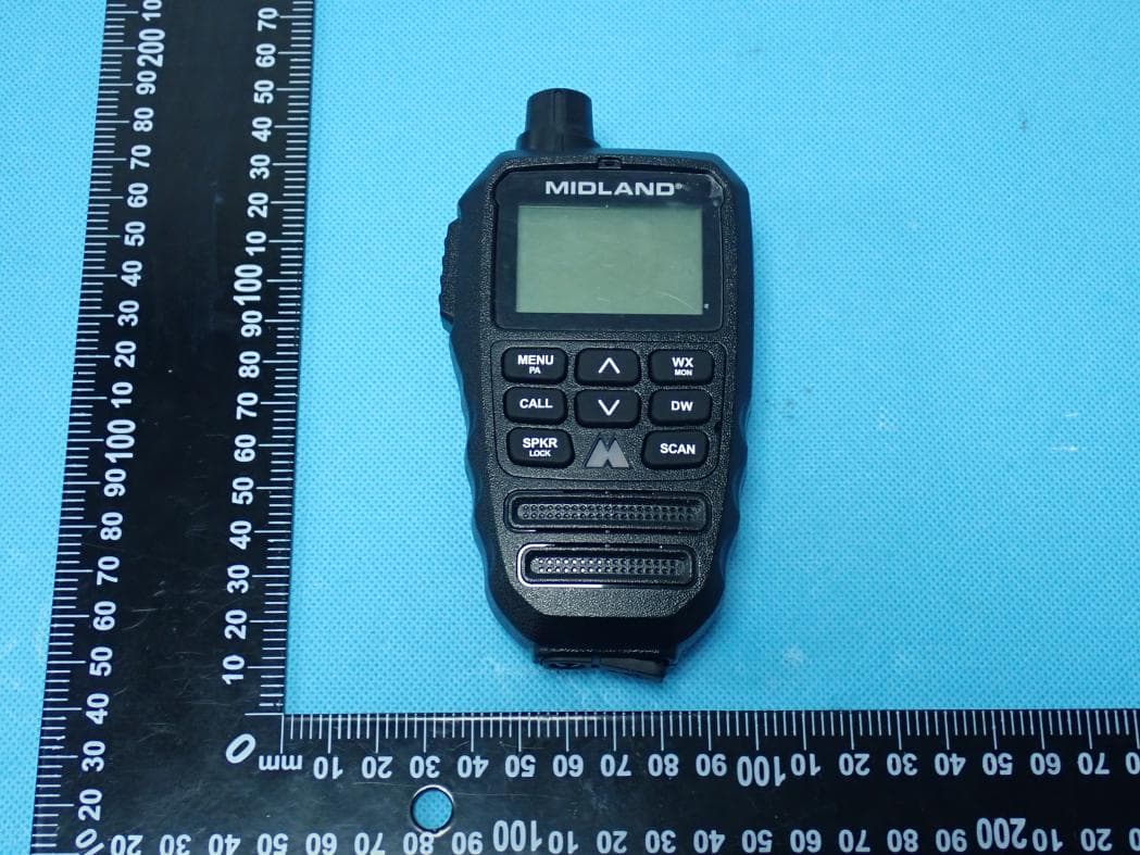
MMAMXMC95
Jun 10, 2026Wireless Bluetooth Microphone
Equipment Class
JAB - Part 15 Class B Digital Device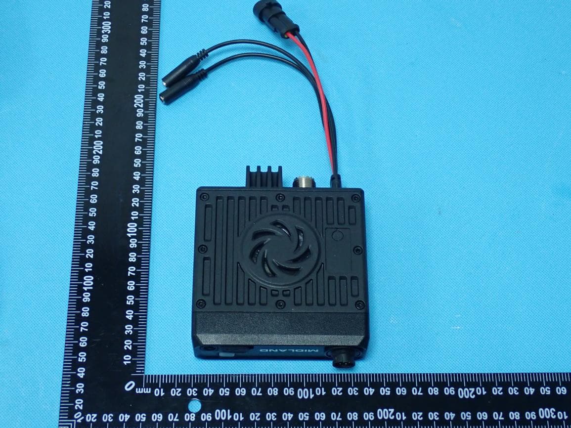
MMAMXT295
Jun 08, 2026GMRS Radio
Equipment Class
TNF - Licensed Non-Broadcast Transmitter Held to Face
MMACLIPTALK
Apr 27, 2026Transceiver
Equipment Class
DTS - Digital Transmission System
MMABR200S
Jan 13, 2026BUSINESS BAND TWO-WAY RADIO
Equipment Class
TNF - Licensed Non-Broadcast Transmitter Held to Face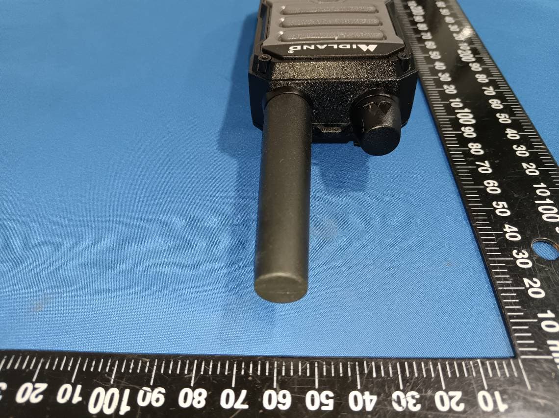
MMAGXT67
Oct 29, 2023GMRS RADIO
Equipment Class
TNF - Licensed Non-Broadcast Transmitter Held to Face