MMASP440UHF HANDHELD TRANSCEIVER
Midland Radio Corporation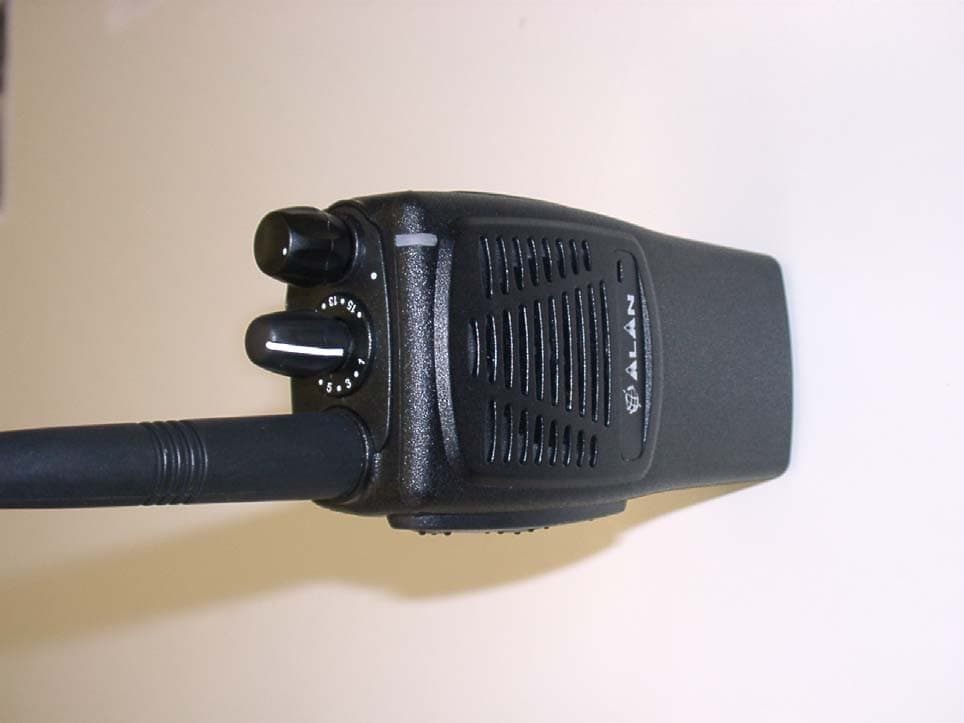
Click to zoom
Application Details
- Equipment Class
- TNB - Licensed Non-Broadcast Station Transmitter
- Date of Grant
- Nov 23, 2004
- Application Purpose
- Original Equipment
- Date of Application
- Nov 23, 2004
- Equipment Note
- UHF HANDHELD TRANSCEIVER
- Frequency Range
- 440.00000000 - 470.00000000
- Company
- Midland Radio Corporation
- Country
- United States
Documents & Files
Document Text
Text extracted from the exhibit documents filed with the FCC. Open a document above to read the original.
Users Manual
80-106/80-406 User manual Page. 1 80-106 VHF Handheld Transceiver 80-406 UHF Handheld Transceiver User’s Manual Copyright © 2004 by Midland Radio Corporation; all rights reserved. PN: 80-106406 Note: Change ALAN logo to Midland logo or just leave logo area blank. 80-106/80-406 User manual Page. 2 FCC RF EXPOSURE COMPLIANCE REQUIREMENTS FOR OCCUPATIONAL USE ONLY The Federal Communications Commission (FCC), within its action in General Docket 93-62, November 7, 1997, has adopted a safety standard for human exposure to Radio Frequency (RF) electromagnetic energy emitted by FCC regulated equipment. Midland Radio Corporation subscribes to the same safety standard for the use of its products. Proper operation of this radio will result in user exposure far below the Occupational Safety and Health Act (OSHA) and FCC limits. DO NOT transmit for more than 50% of total use time (50% duty cycle). Transmitting more than 50% of the time can cause FCC RF exposure compliance requirements to be exceeded. • This radio is NOT approved for use by the general population in an uncontrolled environment. This radio is restricted to occupational use, work related operations only where the radio operator must have the knowledge to control the user’s exposure conditions for satisfying the higher exposure limit allowed for occupational use. • When transmitting, hold the radio in a vertical position with its microphone 2 inches (5cm) away from your mouth. • The radio is transmitting when the red LED on the front of the radio is illuminated. You can cause the radio to transmit by pressing the PTT bar on the radio. • When using VOX mode the radios transmitter is automatically activated with your voice by speaking into the microphone. Use caution when using VOX mode. • These are required operating configurations for meeting FCC RF exposure compliance. Falure to observe these restrictions means violation. This device complies with Part 15 of the FCC Rules. Operation is subject to the condition that this device does not cause harmful interference. 80-106/80-406 User manual Page. 3 In this book... FCC RF EXPOSURE COMPLIANCE REQUIREMENTS FOR OCCUPATIONAL USE ONLY ............................. 2 INTRODUCTION..................................................................................................................................................... 4 W ARNING NOTES.................................................................................................................................................. 4 S AFETY................................................................................................................................................................. 4 FCC RF EXPOSURE COMPLIANCE REQUIREMENTS FOR OCCUPATIONAL USE ONLY ............................. 5 CONVENTIONS AND SYMBOLS IN THIS BOOK........................................................................................................ 6 PART NAMES AND THEIR FUNCTIONS ....................................................................................................... 7 T OP...................................................................................................................................................................... 7 F RONT.................................................................................................................................................................. 7 S IDE (LEFT AND RIGHT) ........................................................................................................................................ 8 SETUP .................................................................................................................................................................... 9 U NPACKING.......................................................................................................................................................... 9 A TTACHING/REMOVING THE ANTENNA............................................................................................................... 10 I NSTALLING/REMOVING THE BATTERY PACK...................................................................................................... 10 I NSTALLING/REMOVING THE BELT CLIP.............................................................................................................. 11 C HARGING THE BATTERY PACK.......................................................................................................................... 11 BASIC OPERATIONS ....................................................................................................................................... 12 S WITCHING THE RADIO ON/OFF ........................................................................................................................ 12 A DJUSTING VOLUME........................................................................................................................................... 12 C HANNEL SELECTION......................................................................................................................................... 12 R ECEPTION......................................................................................................................................................... 12 M ONITOR........................................................................................................................................................... 13 T RANSMISSION................................................................................................................................................... 13 T RANSMISSION POWER....................................................................................................................................... 14 6 CTCSS/DCS AND SELECTIVE CALL OPERATION............................................................................................. 14 S CANNING CHANNELS.....................................................…
Text truncated - open the document above for the full version.
Operational Description
Page 2 of 41 2 CIRCUIT DESCRIPTION 2.1 General information The 80-406 has three printed circuit boards. Circuitry is divided in the following sections: • Microprocessor/Control • VCO/Synthesizer • Transmitter • Receiver • Signalling • Battery Refer to the Block Diagram and the Schematics. 2.2 Microprocessor/control The microprocessor Q17 is constantly operating when the radio is turned ON. It is continuously monitoring the keyboard, the PTT line and other internal inputs such as the squelch detect, etc. When a change occurs, the microprocessor makes the appropriate response. The microprocessor is used for control. The Radio emits a beep on channel change and the synthesizer is loaded with the correct frequency information. The microprocessor runs off a 8 MHz oscillator which is composed of X1, C30, C31 and R48. When the radio is first turned on, the microprocessor reads the radio status from the EEPROM Q8. The microprocessor determines the receive frequency codes, then loads the synthesizer via its pins 42 (PLL LE), 46 (PLL CLK) and 43 (PLL DATA). The microprocessor is fitted with an internal program flash memory as well, therefore functions can be customised, if necessary, upon specific request from the customer (fees may apply). 2.3 VCO / Synthesizer (PLL) This section consists of the Temperature-Compensated Crystal Oscillator (TCXO), Voltage Controlled Oscillator(VCO), Synthesizer and the Loop Filter. 2.3.a Temperature-Compensated Crystal Oscillator (TCXO) The reference oscillator (X401) is a temperature compensated crystal- oscillator, RV402 is used to adjust the oscillator on frequency (14.4 MHz) at room temperature (22 Ž). The reference oscillator is held within the specified ±2.5 PPM from -30 to +60°C. 2.3.b Voltage-Controlled Oscillators Only one of the VCOs runs at a time, which is controlled by Q420 and Q17. When the PTT is pressed, Q17 pin 34 goes low (approx. 0V) disabling the receive VCO by the Q420 and biases on Q419 to enable the transmitter VCO. The receive VCO consists of C989-C994, CV901, L926-L428, L933, and Q922-Q923. This VCO oscillates at 45.1 MHz below the programmed receive frequency. The VCO’s oscillating frequency is tuned by the varactor Q923. The tuning voltage is supplied from the output of the Loop Filter. The output of the VCO is AC coupled to the output buffer Q914. The buffered output is coupled to the synthesizer by R558, C530, and C505. The transmitter VCO consists of C980-C985, C987, CV901, L924, L925, L929 and Q916, Q917. This VCO oscillates on the programmed transmit frequency. The VCO’s oscillating frequency is tuned by the varactor Q417. The tuning voltage is supplied from the output of the Loop Filter. The output of the VCO is AC coupled (C979) to the output buffer Q915. The transmit voltage controlled oscillator is directly frequency-modulated and operates on the carrier frequency. In the receive mode, the transmit VCO is disabled and the receive VCO is enabled, producing the receive local oscillator signal at a frequency 45.1 MHz below the incoming receive frequency. The synthesizer is tuned in 5.00 KHz or 6.25 KHz step. 80-106 Service Manual Page 3 of 41 2.3.c Synthesizer The frequency synthesizer is a large scale monolithic synthesizer integrated circuit Q429. The synthesizer IC contains a dual modular prescaler, programmable divide-by-N counter, prescaler control (swallow) counter, reference oscillator, reference divider, phase detector, charge pump and lock detector. Also, included in Q429 are shift registers and control circuits for frequency controls and general device control. RF output from the active VCO is AC coupled to the synthesizer Q429 prescaler input at Pin 8. The divide-by-N counter chain in Q429, consisting of the dual-modulus prescaler, swallow counter and programmable counter, divides the VCO signal down to a frequency very close to 5.00 KHz or 6.25 KHz which is applied to the phase detector. The phase comparator compares the edges of this of this signal with that of the 5.00 KHz or 6.25 KHz reference signal from the reference divider and drives the external charge pump (Q425 and Q426). The synthesizer unlock detector circuit prevents the operation of the transmitter, when the phase lock loop (PLL) is unlocked. The following discussion assumes the unit has been placed in the transmit mode. Q429 lock detector Pin 7 goes high when the PLL is locked. This high level is applied to Pin 21 of the microprocessor Q17. A software timing routing brings the RX/TX line low (Pin 29 of Q17), feeding this signal through the switch/buffer Q15. With the RX/TX line low, Q223A is cut off and Q223B is biases on passing +5VTX to Q431B, it biases on Q430 to pass switched TX B+ to the transmitter amplifier string which enables transmission. When the PLL become unlocked, the lock detector at Q429 Pin7 will begin pulsing low. A RC circuit converts pulsing low to a low level for the microprocessor. The microprocessor then changes the RX/TX line to a high, thus signalling the other transistor switches to drive Q430 into cutoff which disable transmission. Therefore, the transmitter remains disabled while the loop remains out of lock. 2.3.d Loop Filter The Loop Filter, a passive lead-lag filter consisting of R461-R464 and C493-C495, integrates the charge pump output to produce the DC turning voltage for the VCO. One parasitic pole, consisting of R461/C493 and RF chokes L428/L429, prevent modulation of the VCOs by the 5.00 KHz or 6.25 KHz reference energy remaining at the output of the loop filter. Direct FM is obtained for modulating frequencies outside the PLL bandwidth by applying the CTCSS/DCS signals and the pre-emphasized, limited microphone audio to the VCO modulation circuit. The modulation circuit consists of R452, Q421 and C487. 2.4 Transmitter 2.4.a RF Power Amplifier After the PTT is pressed, the +5VTX line switches to approximately 5V. Q919 is turned on enabling transmit VCO. The VCO buffer, pre-driver, driver and power amplifier are biased …
Text truncated - open the document above for the full version.
Parts List/Tune Up Info
Parts List 80-406 Page 25 of 41 Capacitors Part No. NAME & DESCRIPTION Ref 70-138704 CHIP CERAMIC 0.0033UF GRM39 X7R332K 50V PT C1 70-138977 CHIP TANTALUM 1UF 293D105X0016A2T16V C2 70-138898 CHIP CERAMIC 82PF GRM39 COG820J 50V PT C3 70-138979 CHIP TANTALUM 4.7UF 293D475X0010A2T10V C5 70-138704 CHIP CERAMIC 0.0033UF GRM39 X7R332K 50V PT C6 70-138681 CHIP CERAMIC 0.0047UF GRM39 X7R472K 50V PT C7 70-138898 CHIP CERAMIC 82PF GRM39 COG820J 50V PT C8 70-137318 CHIP CERAMIC 0.0068UF GRM39 X7R682J 50V PT C9 70-138960 CHIP CERAMIC 0.0039UF GRM39 X7R392K 50V PT C10 70-137315 CHIP CERAMIC 43PF GRM39 COG430J 50V PT C11 70-137319 CHIP CERAMIC 0.0036UF CL10 X7R362J 25V C12 70-138955 CHIP CERAMIC 0.01UF GRM39 X7R103K 25V C13 70-137320 CHIP CERAMIC 0.002UF GRM39 X7R202J 25V C14 70-138956 CHIP CERAMIC 0.001UF GRM39 X7R102K 50V PT C15 70-138957 CHIP CERAMIC 0.1UF GRM39 X7R104K 16V AT C16 70-138979 CHIP TANTALUM 4.7UF 293D475X0010A2T10V C17 70-137317 CHIP CERAMIC 160PF CL10 X7R161J 50V C18 70-138979 CHIP TANTALUM 4.7UF 293D475X0010A2T10V C19 70-138954 CHIP CERAMIC 0.0018UF GRM39 X7R182K 50V PT C20 70-138956 CHIP CERAMIC 0.001UF GRM39 X7R102K 50V PT C21 70-138956 CHIP CERAMIC 0.001UF GRM39 X7R102K 50V PT C22 70-138956 CHIP CERAMIC 0.001UF GRM39 X7R102K 50V PT C23 70-138956 CHIP CERAMIC 0.001UF GRM39 X7R102K 50V PT C24 70-138956 CHIP CERAMIC 0.001UF GRM39 X7R102K 50V PT C25 70-138956 CHIP CERAMIC 0.001UF GRM39 X7R102K 50V PT C26 70-138957 CHIP CERAMIC 0.1UF GRM39 X7R104K 16V AT C27 70-138956 CHIP CERAMIC 0.001UF GRM39 X7R102K 50V PT C28 70-138703 CHIP CERAMIC 30PF GRM39 COG300J 50V PT C30 70-138703 CHIP CERAMIC 30PF GRM39 COG300J 50V PT C31 70-138955 CHIP CERAMIC 0.01UF GRM39 X7R103K 25V C32 70-138664 CHIP CERAMIC 100PF GRM39 COG101J 50V PT C33 70-138977 CHIP TANTALUM 1UF 293D105X0016A2T16V C34 70-138956 CHIP CERAMIC 0.001UF GRM39 X7R102K 50V PT C35 70-138956 CHIP CERAMIC 0.001UF GRM39 X7R102K 50V PT C36 70-138956 CHIP CERAMIC 0.001UF GRM39 X7R102K 50V PT C37 70-138956 CHIP CERAMIC 0.001UF GRM39 X7R102K 50V PT C38 70-138704 CHIP CERAMIC 0.0033UF GRM39 X7R332K 50V PT C39 70-135417 CHIP TANTALUM 10UF 293D106X06R3A2T6.3V C43 70-135417 CHIP TANTALUM 10UF 293D106X06R3A2T6.3V C44 70-138957 CHIP CERAMIC 0.1UF GRM39 X7R104K 16V AT C45 70-138956 CHIP CERAMIC 0.001UF GRM39 X7R102K 50V PT C46 70-138956 CHIP CERAMIC 0.001UF GRM39 X7R102K 50V PT C47 70-138956 CHIP CERAMIC 0.001UF GRM39 X7R102K 50V PT C48 70-138956 CHIP CERAMIC 0.001UF GRM39 X7R102K 50V PT C50 70-138664 CHIP CERAMIC 100PF GRM39 COG101J 50V PT C51 70-138664 CHIP CERAMIC 100PF GRM39 COG101J 50V PT C52 Parts List 80-406 Page 26 of 41 70-138956 CHIP CERAMIC 0.001UF GRM39 X7R102K 50V PT C53 70-138957 CHIP CERAMIC 0.1UF GRM39 X7R104K 16V AT C54 70-138956 CHIP CERAMIC 0.001UF GRM39 X7R102K 50V PT C55 70-138950 CHIP TANTALUM 0.1UF TCM1V104ASSR 35V C96 70-138955 CHIP CERAMIC 0.01UF GRM39 X7R103K 25V C97 70-138956 CHIP CERAMIC 0.001UF GRM39 X7R102K 50V PT C101 70-138947 CHIP TANTALUM 10UF TSM0J106ASSR 6.3V C106 70-138956 CHIP CERAMIC 0.001UF GRM39 X7R102K 50V PT C108 70-138900 CHIP CERAMIC 220PF GRM39 COG221J 50V PT C110 70-138900 CHIP CERAMIC 220PF GRM39 COG221J 50V PT C111 70-138956 CHIP CERAMIC 0.001UF GRM39 X7R102K 50V PT C112 70-138956 CHIP CERAMIC 0.001UF GRM39 X7R102K 50V PT C113 70-138956 CHIP CERAMIC 0.001UF GRM39 X7R102K 50V PT C118 70-138956 CHIP CERAMIC 0.001UF GRM39 X7R102K 50V PT C119 70-138956 CHIP CERAMIC 0.001UF GRM39 X7R102K 50V PT C120 70-138956 CHIP CERAMIC 0.001UF GRM39 X7R102K 50V PT C121 70-138956 CHIP CERAMIC 0.001UF GRM39 X7R102K 50V PT C122 70-138956 CHIP CERAMIC 0.001UF GRM39 X7R102K 50V PT C123 70-138956 CHIP CERAMIC 0.001UF GRM39 X7R102K 50V PT C124 70-138956 CHIP CERAMIC 0.001UF GRM39 X7R102K 50V PT C125 70-138956 CHIP CERAMIC 0.001UF GRM39 X7R102K 50V PT C126 70-138956 CHIP CERAMIC 0.001UF GRM39 X7R102K 50V PT C127 70-138956 CHIP CERAMIC 0.001UF GRM39 X7R102K 50V PT C128 70-138956 CHIP CERAMIC 0.001UF GRM39 X7R102K 50V PT C129 70-138956 CHIP CERAMIC 0.001UF GRM39 X7R102K 50V PT C133 70-138956 CHIP CERAMIC 0.001UF GRM39 X7R102K 50V PT C134 70-138956 CHIP CERAMIC 0.001UF GRM39 X7R102K 50V PT C135 70-138956 CHIP CERAMIC 0.001UF GRM39 X7R102K 50V PT C136 70-138956 CHIP CERAMIC 0.001UF GRM39 X7R102K 50V PT C137 70-138956 CHIP CERAMIC 0.001UF GRM39 X7R102K 50V PT C138 70-138895 CHIP CERAMIC 47PF GRM39 COG470J 50V PT C139 70-138957 CHIP CERAMIC 0.1UF GRM39 X7R104K 16V AT C141 70-138946 CHIP TANTALUM 4.7UF TSM0J475ASSR 6.3V C150 70-138962 CHIP CERAMIC 0.047UF GRM39 Y5V473Z 25V PT C151 70-138957 CHIP CERAMIC 0.1UF GRM39 X7R104K 16V AT C155 70-138957 CHIP CERAMIC 0.1UF GRM39 X7R104K 16V AT C156 70-138946 CHIP TANTALUM 4.7UF TSM0J475ASSR 6.3V C160 70-138956 CHIP CERAMIC 0.001UF GRM39 X7R102K 50V PT C165 70-138956 CHIP CERAMIC 0.001UF GRM39 X7R102K 50V PT C173 70-138956 CHIP CERAMIC 0.001UF GRM39 X7R102K 50V PT C174 70-138956 CHIP CERAMIC 0.001UF GRM39 X7R102K 50V PT C175 70-138956 CHIP CERAMIC 0.001UF GRM39 X7R102K 50V PT C176 70-138956 CHIP CERAMIC 0.001UF GRM39 X7R102K 50V PT C201 70-138667 CHIP CERAMIC 15PF GRM39 COG150J 50V PT C202 70-138668 CHIP CERAMIC 18PF GRM39 COG180J 50V PT C203 70-138956 CHIP CERAMIC 0.001UF GRM39 X7R102K 50V PT C204 70-138957 CHIP CERAMIC 0.1UF GRM39 X7R104K 16V AT C205 70-138947 CHIP TANTALUM 10UF TSM0J106ASSR 6.3V C206 70-138956 CHIP CERAMIC 0.001UF GRM39 X7R102K 50V PT C207 Parts List 80-406 Page 27 of 41 70-138957 CHIP CERAMIC 0.1UF GRM39 X7R104K 16V AT C208 70-138957 CHIP CERAMIC 0.1UF GRM39 X7R104K 16V AT C209 70-138900 CHIP CERAMIC 220PF GRM39 COG221J 50V PT C210 70-138900 CHIP CERAMIC 220PF GRM39 COG221J 50V PT C211 70-138959 CHIP CERAMIC 0.22UF GRM40 X7R224K 16V C213 70-138956 CHIP CERAMIC 0.001UF GRM39 X7R102K 50V PT C214 70-138959 CHIP CERAMIC 0.22UF GRM40 X7R224K 16V C215 70-138664 CHIP CERAMIC 100PF GRM39 COG101J 50V PT C216 70-138957 CHIP CERAMIC 0.1UF GRM39 X7R104K 16V AT C217 70-138900 CHIP CERAMIC 220PF GRM39 COG221J 50V PT C218 70-138956 CHIP CERAMIC 0.001UF GRM39 X7R102K 50V PT C220 70-138959 CHIP …
Text truncated - open the document above for the full version.
RF Exposure Info
© 2004 Celltech Labs Inc. 1 of 20 Test Report S/N: 101504MMA-T571-S90U Test Date(s): October 16-17, 2004 Test Type: FCC/IC SAR Evaluation Performed By: Spencer Watson Compliance Technologist Celltech Labs Inc. Reviewed By: Russell W. Pipe Senior Compliance Technologist Celltech Labs Inc. Celltech Labs Inc. declares under its sole responsibility that this wireless portable device has demonstrated compliance with the Specific Absorption Rate (SAR) RF exposure requirements specified in FCC 47 CFR §2.1093 and Health Canada’s Safety Code 6. The device was tested in accordance with the measurement standards and procedures specified in FCC OET Bulletin 65, Supplement C (Edition 01-01) and Industry Canada RSS-102 Issue 1 (Provisional) for the Occupational / Controlled Exposure environment. All measurements were performed in accordance with the SAR system manufacturer recommendations. I attest to the accuracy of data. All measurements were performed by me or were made under my supervision and are correct to the best of my knowledge and belief. I assume full responsibility for the completeness of these measurements and vouch for the qualifications of all persons taking them. This test report shall not be reproduced partially, or in full, without the prior written approval of Celltech Labs Inc. The results and statements contained in this report pertain only to the device(s) evaluated. DECLARATION OF COMPLIANCE SAR RF EXPOSURE EVALUATION Test Lab CELLTECH LABS INC. Testing and Engineering Services 1955 Moss Court Kelowna, B.C. Canada V1Y 9L3 Phone: 250-448-7047 Fax: 250-448-7046 e-mail: [email protected] web site: www.celltechlabs.com Applicant Information Midland Radio Corporation 1120 Clay Street North Kansas City, Missouri 64116 United States FCC IDENTIFIER: MMASP400 IC IDENTIFIER: 3690A-SP440 Model(s): SP-440 Rule Part(s): FCC 47 CFR §2.1093; IC RSS-102 Issue 1 (Provisional) Test Procedure(s): FCC OET Bulletin 65, Supplement C (Edition 01-01) Device Classification: Licensed Non-Broadcast Transmitter Held to Face (TNF) Device Type: Portable UHF PTT Radio Transceiver Modulation: FM (UHF) TX Frequency Range: 440 - 470 MHz Max. RF Output Power Tested: 36.48 dBm Conducted (440.1 MHz) 36.36 dBm Conducted (455.1 MHz) 36.22 dBm Conducted (469.9 MHz) Antenna Type(s) Tested: Stubby (P/N: ACC-104UW) Battery Type(s) Tested: NiMH 7.2 V, 1300 mAh (P/N: BP0513) Body-Worn Accessories Tested: Plastic Belt-Clip with Metal Spring (P/N: 81BC1) Speaker-Microphone (P/N: 70-M45WP) Max. SAR Levels Evaluated: Face-held: 3.66 W/kg (50% Duty Cycle) Body-worn: 5.23 W/kg (50% Duty Cycle) © 2004 Celltech Labs Inc. 2 of 20 Test Report S/N: 101504MMA-T571-S90U Test Date(s): October 16-17, 2004 Test Type: FCC/IC SAR Evaluation TABLE OF CONTENTS 1.0INTRODUCTION.....................................................................3 2.0DESCRIPTION OF DUT............................................................ 3 3.0SAR MEASUREMENT SYSTEM................................................ 4 4.0MEASUREMENT SUMMARY..................................................... 5 5.0DETAILS OF SAR EVALUATION............................................... 6 6.0EVALUATION PROCEDURES................................................... 6 7.0SYSTEM PERFORMANCE CHECK............................................. 7 8.0SIMULATED EQUIVALENT TISSUES.......................................... 8 9.0SAR SAFETY LIMITS............................................................... 8 10.0ROBOT SYSTEM SPECIFICATIONS........................................... 9 11.0PROBE SPECIFICATION (ET3DV6)........................................... 10 12.0PLANAR PHANTOM................................................................. 10 13.0VALIDATION PHANTOM........................................................... 10 14.0DEVICE HOLDER.................................................................... 10 15.0TEST EQUIPMENT LIST............................................................ 11 16.0MEASUREMENT UNCERTAINTIES............................................. 12-13 17.0REFERENCES.........................................................................14 APPENDIX A - SAR MEASUREMENT DATA............................................... 15 APPENDIX B - SYSTEM PERFORMANCE CHECK DATA............................ 16 APPENDIX C - SYSTEM VALIDATION PROCEDURES................................. 17 APPENDIX D - PROBE CALIBRATION...................................................... 18 APPENDIX E - MEASURED FLUID DIELECTRIC PARAMETERS................... 19 APPENDIX F - SAR TEST SETUP & DUT PHOTOGRAPHS.......................... 20 © 2004 Celltech Labs Inc. Midland Radio Corporation FCC ID: MMASP400 3 of 20 Portable UHF PTT Radio Transceiver (440-470 MHz) Test Report S/N: 101504MMA-T571-S90U Test Date(s): October 16-17, 2004 Test Type: FCC/IC SAR Evaluation This measurement report demonstrates compliance of the Midland Radio Corporation Model: SP-440 Portable UHF PTT Radio Transceiver FCC ID: MMASP400 with the SAR (Specific Absorption Rate) RF exposure requirements specified in FCC 47 CFR §2.1093 (see reference [1]), and Health Canada’s Safety Code 6 (see reference [2]) for the Occupational / Controlled Exposure environment. The measurement procedures described in FCC OET Bulletin 65, Supplement C (Edition 01-01) (see reference [3]) and IC RSS-102 Issue 1 (Provisional) (see reference [4]), were employed. A description of the product, operating configuration, detailed summary of the test results, methodology and procedures used in the evaluation, equipment used, and the various provisions of the rules are included within this test report. FCC Rule Part(s) 47 CFR §2.1093 IC Rule Part(s) RSS-102 Issue 1 (Provisional) Test Procedure(s) FCC OET Bulletin 65, Supplement C (01-01) Device Type Portable UHF PTT Radio Transceiver FCC IDENTIFIER MMASP400 IC IDENTIFIER 3690A-SP440 Model(s) SP-440 Serial No. 040700002 Production Unit Modulation FM (UHF) Tx Frequency Range 440 - 470 MHz 36.48 dBm C…
Text truncated - open the document above for the full version.
Schematics
Hp-406 PP_REV_2.sch-1 - Mon May 17 11:20:34 2004 Hp-406 PP_REV_2.sch-2 - Mon May 17 11:20:36 2004 Hp-406 PP_REV_2.sch-3 - Mon May 17 11:20:37 2004
Test Report
TIMCO ENGINEERING INC. 849 NW State Road 45 Newberry, Florida 32669 http://www.timcoengr.com 888.472.2424 F 352.472.2030 email: [email protected] APPLICANT: MIDLAND RADIO CORPORATION FCC ID: MMASP440 REPORT #: M\MidlandRadio_MMA\1767AUT4\1767AUT4TestReport.doc COVER SHEET Test Report Product Name: UHF TRANSCEIVER FCC ID: MMASP440 Applicant: MIDLAND RADIO CORPORATION 1120 CLAY STREET NORTH KANSAS CITY, MO. 64116 Date Receipt: OCTOBER 26, 2004 Date Tested: NOVEMBER 19, 2004 TIMCO ENGINEERING INC. 849 NW State Road 45 Newberry, Florida 32669 http://www.timcoengr.com 888.472.2424 F 352.472.2030 email: [email protected] APPLICANT: MIDLAND RADIO CORPORATION FCC ID: MMASP440 REPORT #: M\MidlandRadio_MMA\1767AUT4\1767AUT4TestReport.doc TABLE OF CONTENTS APPLICANT: MIDLAND RADIO CORPORATION FCC ID: MMASP440 TABLE OF CONTENTS LIST TEST REPORT: PAGE 1...........GENERAL INFORMATION & TECHNICAL DESCRIPTION PAGE 2...........TECHNICAL DESCRIPTION CONTINUED RF POWER OUTPUT PAGE 3...........MODULATION CHARACTERISTICS AUDIO FREQUENCY RESPONSE PAGE 4...........AUDIO LOW PASS FILTER PLOT PAGE 5...........MODULATION LIMITING PLOTS PAGE 6-7.........OCCUPIED BANDWIDTH PAGE 8-9.........OCCUPIED BANDWIDTH PLOTS PAGE 10..........SPURIOUS EMISSIONS AT ANTENNA TERMINALS PAGE 11..........METHOD OF MEASURING SPURIOUS EMISSIONS AT ANTENNA TERMINALS PAGE 12-14.......FIELD STRENGTH OF SPURIOUS EMISSIONS PAGE 15..........METHOD OF MEASURING RADIATED SPURIOUS EMISSIONS PAGE 16..........FREQUENCY STABILITY PAGE 17-18.......TRANSIENT FREQUENCY STABILITY PAGE 19-22.......TRANSIENT FREQUENCY RESPONSE PLOTS PAGE 23-28.......EQUIPMENT LIST EXHIBITS CONTAINING: SAR REPORT BLOCK DIAGRAM SCHEMATIC PARTS LIST USERS MANUAL LABEL SAMPLE LABEL LOCATION EXTERNAL PHOTOGRAPHS INTERNAL PHOTOGRAPHS TUNING PROCEDURE OPERATIONAL DESCRIPTION TEST SET UP PHOTOGRAPH TIMCO ENGINEERING INC. 849 NW State Road 45 Newberry, Florida 32669 http://www.timcoengr.com 888.472.2424 F 352.472.2030 email: [email protected] APPLICANT: MIDLAND RADIO CORPORATION FCC ID: MMASP440 REPORT #: M\MidlandRadio_MMA\1767AUT4\1767AUT4TestReport.doc Page 1 of 28 GENERAL INFORMATION REQUIRED FOR CERTIFICATION OF A LICENSED TRANSMITTER 2.1033(c)(1)(2) MIDLAND RADIO CORPORATION will manufacture the FCCID: MMASP440 UHF TRANSCEIVER in quantity, for use under FCC RULES PART 90. MIDLAND RADIO CORPORATION 1120 CLAY STREET NORTH KANSAS CITY, MO. 64116 2.1033(c) TECHNICAL DESCRIPTION 2.1033(c)(3) Instruction book. A draft copy of the instruction manual is included. 2.1033(c)(4) Type of Emission: 14K4F3E 90.209 90.207 Bn = 2M + 2DK M = 3000 D = 4200 Bn = 2(3000) + 2(4200) = 14.4k 2.1033(c)(5) Frequency Range: 440 - 470 MHz 90.209 (b)(5) 2.1033(c)(4) Type of Emission: 11K0F3E 90.209 90.207 Bn = 2M + 2DK M = 3000 D = 2500 Bn = 2(3000) + 2(2500) = 11k 2.1033(c)(5) Frequency Range: 440 - 470 MHz 90.209 (b)(5) 2.1033(c)(6)(7) Power Output shall not exceed 59 Watts into a 50 ohm 90.205 resistive load. There are no user power controls. 2.1033(c)(8) DC Voltages and Current into Final Amplifier: POWER INPUT: FINAL AMPLIFIER ONLY INPUT POWER – HIGH: (7.2V)(2.2A) = 15.84 Watts 2.1033(c)(9) Tune-up procedure. The tune-up procedure is included. 2.1033(c)(10) Complete Circuit Diagrams: The circuit diagram is included. The block diagram is included. TIMCO ENGINEERING INC. 849 NW State Road 45 Newberry, Florida 32669 http://www.timcoengr.com 888.472.2424 F 352.472.2030 email: [email protected] APPLICANT: MIDLAND RADIO CORPORATION FCC ID: MMASP440 REPORT #: M\MidlandRadio_MMA\1767AUT4\1767AUT4TestReport.doc Page 2 of 28 2.1033(c)(11) Description of all circuitry and devices provided for determining and stabilizing frequency is included in the circuit description. 2.1033(c)(12) A photograph or drawing of the equipment identification label is included. 2.1033(c)(13) Photographs of the equipment of sufficient clarity to reveal equipment construction and layout and label location are included. 2.1033(c)(14) Digital Modulation is not allowed 2.1033(c)(15) The data required for 2.1046 through 2.1057 is submitted below. 2.1046(a) RF POWER OUTPUT RF power is measured by connecting a 50-ohm, resistive wattmeter to the RF output connector. With a nominal battery voltage, and the transmitter properly adjusted the RF output measures: OUTPUT POWER: HIGH: 4 Watts LOW: .8 Watts Transmitter under Test Power Meter Audio Oscillator TIMCO ENGINEERING INC. 849 NW State Road 45 Newberry, Florida 32669 http://www.timcoengr.com 888.472.2424 F 352.472.2030 email: [email protected] APPLICANT: MIDLAND RADIO CORPORATION FCC ID: MMASP440 REPORT #: M\MidlandRadio_MMA\1767AUT4\1767AUT4TestReport.doc Page 3 of 28 2.1047(a)(b) Modulation characteristics : AUDIO FREQUENCY RESPONSE The audio frequency response was measured in accordance with TIA/EIA Specification 603. A curve or equivalent data showing the frequency response of the audio modulating circuit over a range of 100 – 5000Hz shall be submitted. The audio frequency response curve is shown below. Audio Frequency Response Plot -30 +10 -20 -10 +0 d B 100 4k 200 300 400 500 700 1k 2k 3k Hz TIMCO ENGINEERING INC. 849 NW State Road 45 Newberry, Florida 32669 http://www.timcoengr.com 888.472.2424 F 352.472.2030 email: [email protected] APPLICANT: MIDLAND RADIO CORPORATION FCC ID: MMASP440 REPORT #: M\MidlandRadio_MMA\1767AUT4\1767AUT4TestReport.doc Page 4 of 28 2.1047(a) Voice modulated communication equipment: For equipment required to have an audio low-pass filter, a curve showing the frequency response of the filter, or of all the circuitry installed between the modulation limiter and the modulated stage shall be submitted. Audio Low Pass Filter Plot -30 +10 -20 -10 +0 d B 2k 20k 3k 4k 5k 6k 7k 8k 10k Hz TIMCO ENGINEERING INC. 849 NW State Road 45 Newberry, Florida 32669 http://www.timcoengr.com 888.472.2424 F 352.472.2030 email: sid@…
Text truncated - open the document above for the full version.
Contact Information
Applicant
Butch Rittmann(Director of Operations)
Test Firm
Timco Engineering, Inc.Sid Sanders
Technical Specifications
| # | Rule Parts | Frequency Range | Power Output | Emission | Tolerance |
|---|---|---|---|---|---|
| 4 | 9 | 440 MHz - 470 MHz | 800.00 mW | 11K0F3E | 1.5 ppm |
Other Applications from Midland Radio Corporation
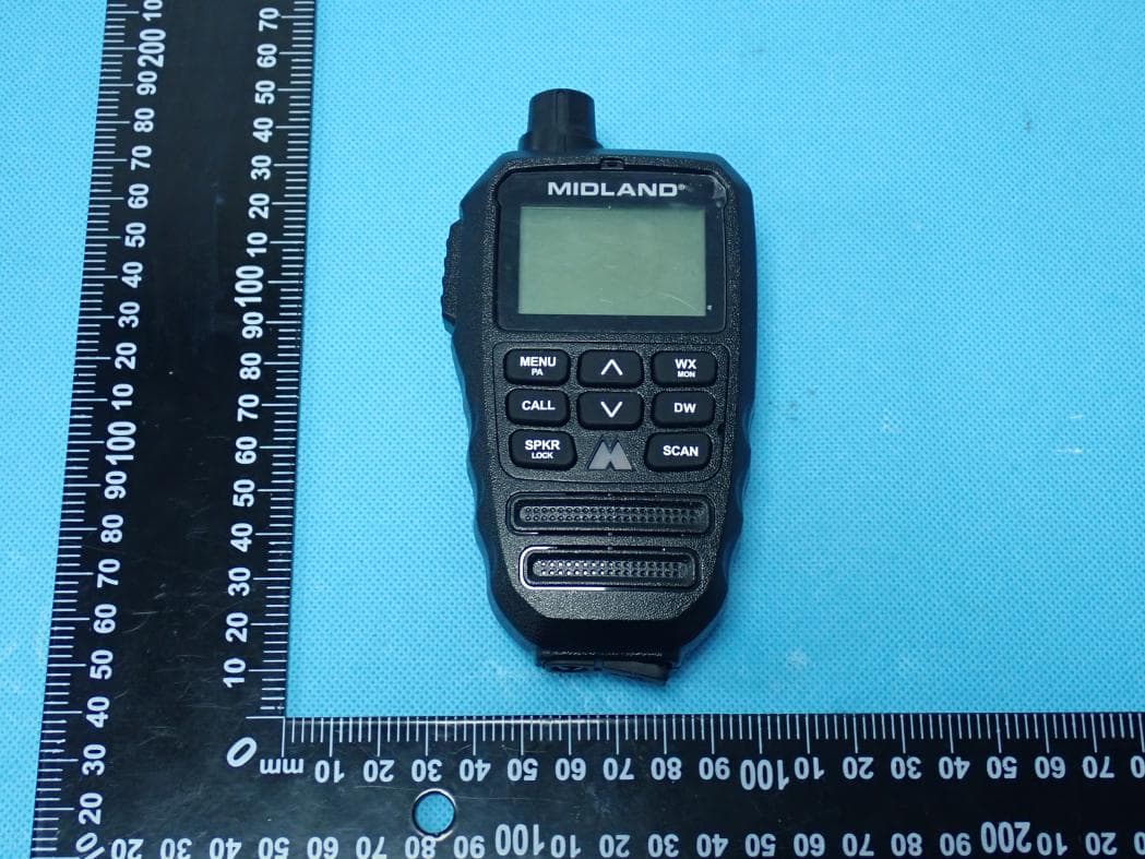
MMAMXMC95
Jun 10, 2026Wireless Bluetooth Microphone
Equipment Class
JAB - Part 15 Class B Digital Device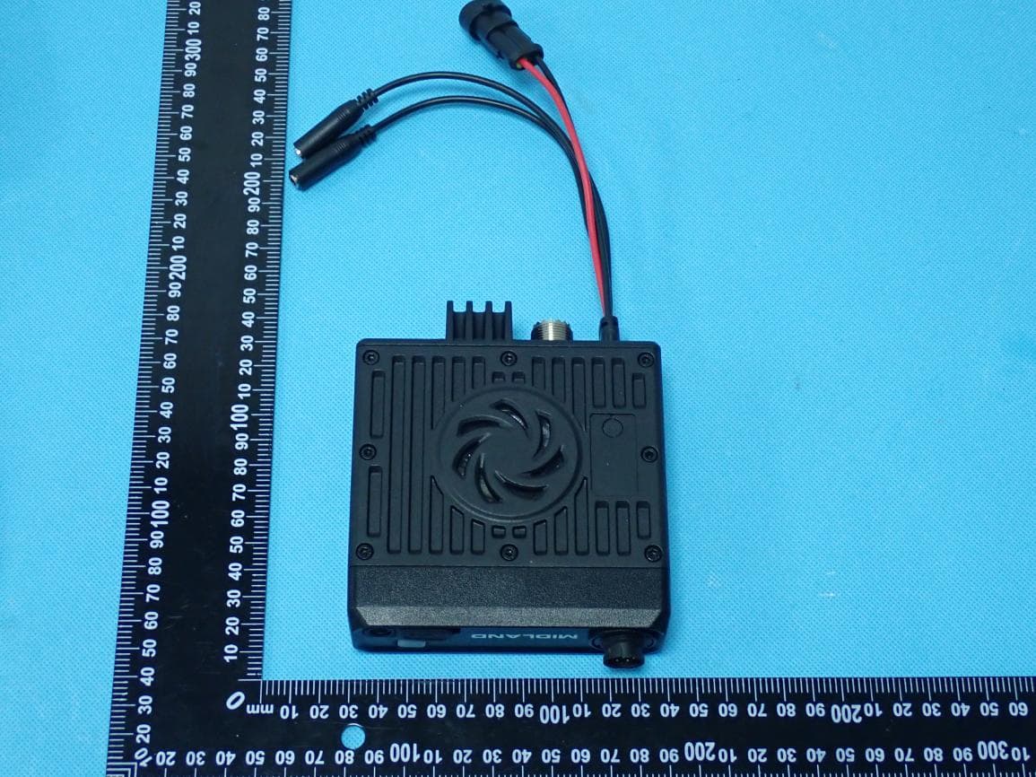
MMAMXT295
Jun 08, 2026GMRS Radio
Equipment Class
TNF - Licensed Non-Broadcast Transmitter Held to Face
MMACLIPTALK
Apr 27, 2026Transceiver
Equipment Class
DTS - Digital Transmission System
MMABR200S
Jan 13, 2026BUSINESS BAND TWO-WAY RADIO
Equipment Class
TNF - Licensed Non-Broadcast Transmitter Held to Face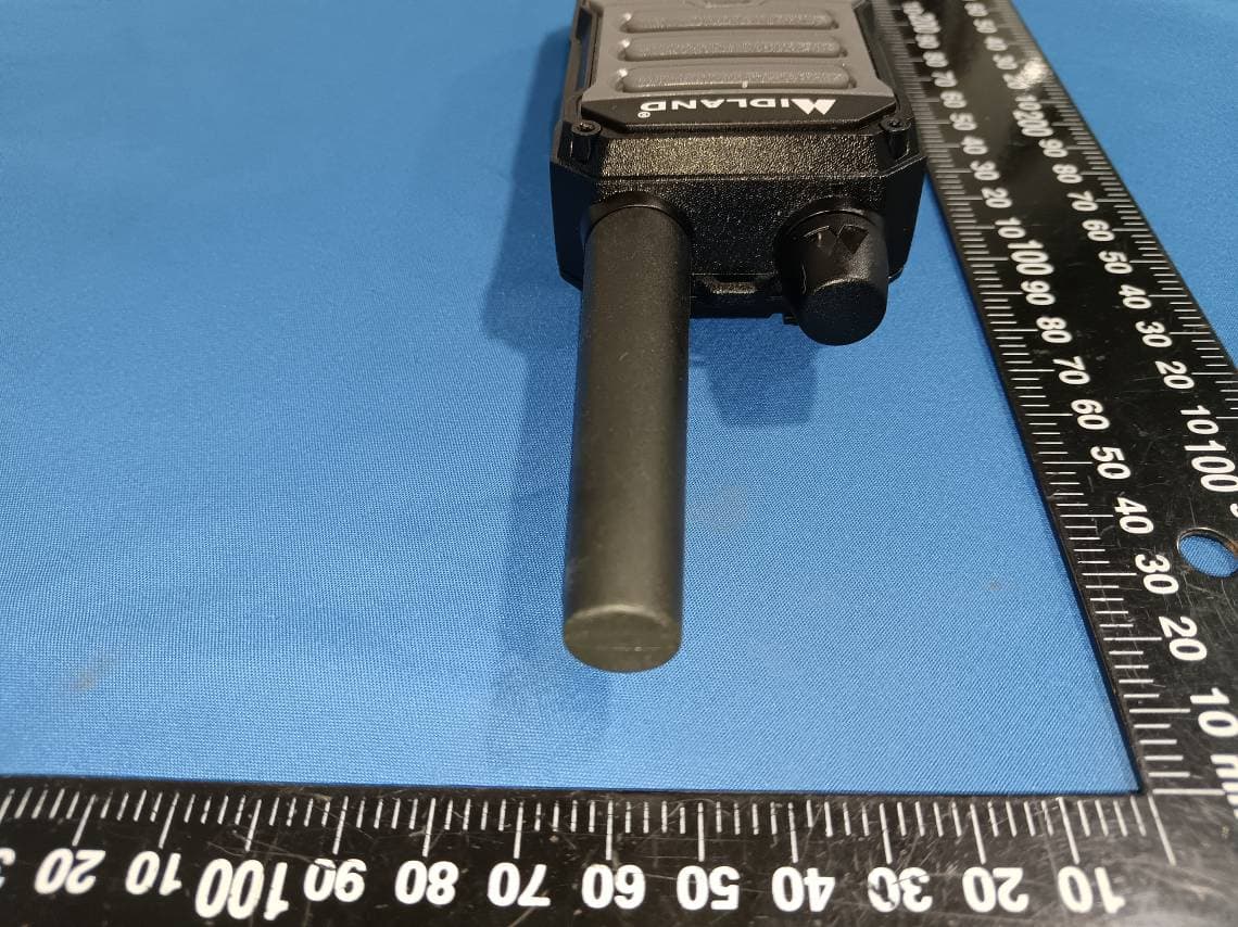
MMAGXT67
Oct 29, 2023GMRS RADIO
Equipment Class
TNF - Licensed Non-Broadcast Transmitter Held to Face