MQXA440Wireless Telemetry Modem
Adcon Telemetry Inc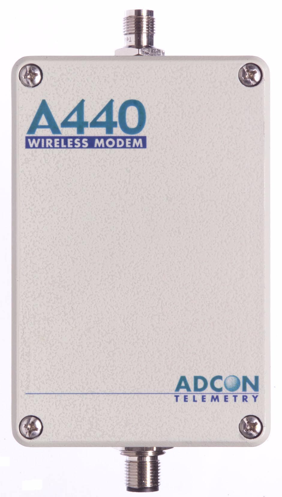
Click to zoom
Application Details
- Equipment Class
- TNB - Licensed Non-Broadcast Station Transmitter
- Date of Grant
- May 22, 2001
- Application Purpose
- Original Equipment
- Date of Application
- May 15, 2001
- Equipment Note
- Wireless Telemetry Modem
- Frequency Range
- 430.00000000 - 470.00000000
- Company
- Adcon Telemetry Inc
- Country
- United States
Documents & Files
Document Text
Text extracted from the exhibit documents filed with the FCC. Open a document above to read the original.
Users Manual
ADCON TELEMETRY SMART WIRELESS SOLUTIONS A440 Wireless Modem Technical Reference Manual ADCON TELEMETRY ADCON TELEMETRY AG INKUSTRASSE 24 A-3400 KLOSTERNEUBURG AUSTRIA TEL: +43 (2243) 38 280-0 FAX: +43 (2243) 38 280-6 http://www.adcon.at ADCON TELEMETRY INC 1001 YAMATO ROAD SUITE #305, BOCA RATON FL 33431 USA TEL: +1 (561) 989-5309 FAX: +1 (561) 989-5310 http://www.adcon.com ADCON TELEMETRY SRL BD. ION IONESCU DELABRAD 8 R-71592 BUCHAREST ROMANIA TEL: +40 (1) 490-6083 FAX: +40 (1) 490-6086 http://www.adcon.ro Proprietary Notice: The Adcon logo, the A730 series, A720 series and addIT™, A440 and add- WAVE, addVANTAGE® and AgroExpert™ are trademarks or registered trade- marks of Adcon Telemetry AG. All other registered names used throughout this publication are trademarks of their respective owners. This publication contains confidential information, property of Adcon Teleme- try AG. Disclosure to third parties of the information contained herein is pro- hibited. Neither the whole nor any part of the information contained in this publication may be reproduced in any material form except with the prior writ- ten permission of Adcon Telemetry AG. Release 1.0, February, 2001 Copyright © 2001 by Adcon Telemetry AG. All rights reserved. 3 Table of Contents Introduction ____________________________________________________7 About the A440 ______________________________________________________________ 7 Hardware _______________________________________________________9 Overview_____________________________________________________________________ 9 The Modem Interfaces ________________________________________________________________ 10 The Microcontroller and the Power Conditioning Sections _________________________________ 10 The Power Supply and Serial Interface ___________________________________________________ 13 External Power Supply_________________________________________________________________ 13 Specifications________________________________________________________________13 PCB Parts Placement (A440) __________________________________________________15 Bills of Materials _____________________________________________________________15 A440MB _____________________________________________________________________________ 16 A440 Device’s Photographs___________________________________________________21 The A431 Radio Module _______________________________________ 27 About the A431 Radio Module ________________________________________________27 Functional description ________________________________________________________27 Receiver Section ______________________________________________________________________ 27 Transmitter Section____________________________________________________________________ 28 Manufacturing Issues _________________________________________________________30 Marking and labeling issues ____________________________________________________________ 30 4 Alignment Range and Switching Range __________________________________________________ 30 Tuning Procedure _____________________________________________________________________ 31 Setting Up the Default Parameters ______________________________________________________ 31 Commands valid for all bands ____________________________________________________ 32 Commands required for band 1 __________________________________________________ 32 Commands required for band 2 __________________________________________________ 32 Commands required for band 3 __________________________________________________ 32 Commands required for band 4 __________________________________________________ 32 Definitions ___________________________________________________________________________ 33 Test Equipment Settings _______________________________________________________________ 34 Network Analyzer (HP 8712 or equivalent)_____________________________________________ 34 Service Monitor (Rohde & Schwarz CMS50 or equivalent) _______________________________ 34 Trimming Elements ____________________________________________________________________ 35 Adjusting the Receiver Front End _______________________________________________________ 35 Adjusting the VCOs ___________________________________________________________________ 36 Adjusting the Crystal Reference _________________________________________________________ 37 Checking the Receiver Parameters ______________________________________________________ 37 Checking the Transmitter Parameters ____________________________________________________ 37 Data Transfer Check ___________________________________________________________________ 38 PCB Parts Placement_________________________________________________________ 39 Bill of Materials (A431) _______________________________________________________ 41 Frequency Reference Specifications ___________________________________________ 45 A431 Module’s Photographs _________________________________________________ 46 Software ______________________________________________________ 49 Short Description ____________________________________________________________ 49 Tasks _______________________________________________________________________ 49 Controlling the Unit__________________________________________________________ 50 Serial Communication Protocol _________________________________________________________ 50 General Format of a Command _________________________________________________________ 50 General Format of an Answer ___________________________________________________________ 51 Commands ___________________________________________________________________________ 51 CMDS _____________________________________________________51 TIME _____________________________________________________51 SR ____________________________________________________________________________ 52 BL ____________________________________________________________________________ 52 FREQ _________________________________________________________________________ 53 DATA ____________________…
Text truncated - open the document above for the full version.
External Photos
21 A440MB 2.5.A440 Device’s Photographs Figure 6. A440, Front view. 551XTAL-MC306 32.76KH z MC-306X1Seiko Epson 56SMD Header1SLY8/SMD/055/4 S2mmJ1Fischer Elektronik 57Jumper1CAB102mmto J1Fischer Elektronik PosDescriptionCountComponent NameValuePatternRef DesManufacturer 22 Hardware Figure 7. A440, Back view. 23 A440MB Figure 8. A440, Top view. Figure 9. A440, Bottom view. 24 Hardware Figure 10. A440, Left and Right views.
ID Label/Location Info
22 Hardware Figure 7. A440, Back view.
Internal Photos
25 A440MB Figure 11. A440, Case opened. Figure 12. A440 Motherboard, top view. 26 Hardware Figure 13. A440 Motherboard, bottom view.
Test Report
TABLE OF CONTENTS LIST APPLICANT: ADCON TELEMETRY INC. FCC ID: MQXA440 TEST REPORT: PAGE 1......COVER SHEET - GENERAL INFORMATION & TECHNICAL DESCR. PAGE 2......TECHNICAL DESCRIPTION CONTINUED & RF POWER OUTPUT PAGE 3......RF POWER OUTPUT, MOD CHARACTERISTICS & OCCUPIED B/W PAGE 4......OCCUPIED BANDWIDTH CONTINUED PAGE 5......OCCUPIED BANDWIDTH PLOT – CW PAGE 6......OCCUPIED BANDWIDTH PLOT – 25 kHz PAGE 7......OCCUPIED BANDWIDTH PLOT – 12.5 kHz PAGE 8......SPURIOUS EMISSIONS AT ANTENNA TERMINALS PAGE 9......METHOD OF MEASURING SPURIOUS EMISSIONS AT ANTENNA TERM. PAGE 10......FIELD STRENGTH OF SPURIOUS EMISSIONS PAGE 11......METHOD OF MEASURING RADIATED SPURIOUS EMISSIONS PAGE 12......FREQUENCY STABILITY PAGE 13-14...TRANSIENT FREQUENCY STABILITY PAGE 15-16...TRANSIENT FREQUENCY RESPONSE PLOTS – 12.5 kHz PAGE 17......LIST OF TEST EQUIPMENT EXHIBITS CONTAINING: EXHIBIT 1A........FCC ID LABEL SAMPLE EXHIBIT 1B........SKETCH OF LOCATION EXHIBIT 2.........SCHEMATIC EXHIBIT 3.........BLOCK DIAGRAM EXHIBIT 4.........CRYSTAL SPECIFICATION EXHIBIT 5.........OPERATIONAL DESCRIPTION EXHIBIT 6.........EXTERNAL PHOTOGRAPHS EXHIBIT 7.........INTERNAL PHOTOGRAPHS EXHIBIT 8.........TUNING PROCEDURE EXHIBIT 9.........TECHNICAL MANUAL APPLICANT: ADCON TELEMETRY INC. FCC ID: MQXA440 REPORT #: T:\CUS\A\ADCON\222AU1\222AU1RPT.DOC PAGE: TABLE OF CONTENTS GENERAL_INFORMATION_REQUIRED FOR_TYPE_ACCEPTANCE 2.1033 ADCON TELEMETRY INC. will sell the (c)(1)(2) MODEL NO. MQXA440 VHF transceiver in quantity, for use under FCC RULES PART 22 & 90. 2.1033 (c) TECHNICAL DESCRIPTION 2.1033 (3) User Manual See Exhibit 14 2.1033 (4) Type of Emission: 7K3F2D For 25KHz 7K3F2D For 12.5KHz For 25KHz & 12kHz Bn = 2M + 2DK M = 4,000 Bits per second D = 1.65KHz (Peak Deviation) K = 1 Bn = 2(4000/2) + 2(1.65K)(1) = 4.0K + 3.3K = 7.3k ALLOWED AUTHORIZED BANDWIDTH = 20.00KHz. For 12.5KHz ALLOWED AUTHORIZED BANDWIDTH = 11.25KHz. 90.209(b)(5) 2.1033 (5) Frequency Range: 430-470 MHz (6) Power Range and Controls:There are NO user Power controls. (7) Maximum Output Power Rating: 0.5 Watts , into a 50 ohm resistive load. (8) DC Voltages and Current into Final Amplifier: POWER INPUT FINAL AMPLIFIER ONLY Vce = 7.8 Volts IC = .55 A (9) Tune-up procedure. The tune-up procedure is given in EXHIBIT 8. APPLICANT: ADCON TELEMETRY INC. FCC ID: MQXA440 REPORT #: T:\CUS\A\ADCON\222AU1\222AU1RPT.DOC PAGE #: 1 2.1033 (10) Complete Circuit Diagrams: The circuit diagram is included as EXHIBIT 2. The block diagram is included as EXHIBIT 3. (11) Function of each electron tube or semiconductor device or other active circuit device: -SEE EXHIBIT 14. (8) Instruction book. The instruction manual is included as EXHIBIT 14. (10) Description of all circuitry and devices provided for determining and stabilizing frequency is included in the circuit description in the instruction manual. 2.1033(c)(11) A photograph or drawing of the equipment identification label is shown in Exhibit 1. 2.1033(c)(12) Photographs of the equipment of sufficient clarity to reveal equipment construction and layout and label location are shown in Exhibit 6-7. 2.1033(c)(13) For equipment employing digital modulation, a detail description of the modulation technique. This UUT uses FSK to modulate the transmitter. 2.1033(c)(14) data required for 2.1046 to 2.1057 SEE Below 2.1046(a) RF_power_output . RF power is measured by connecting a 50 ohm, re- sistive wattmeter to the RF output connector. With a nominal battery voltage of 7.8 VDC, and the transmitter properly adjusted the RF output measures: POWER OUTPUT INPUT POWER - HIGH: (7.8V)(0.550A) = 1.7 Watts INPUT POWER – LOW: (7.8V)(0.2A) = 1.56 Watts OUTPUT POWER: HIGH - .5 Watts LOW - .038 Watts APPLICANT: ADCON TELEMETRY INC. FCC ID: MQXA440 REPORT #: T:\CUS\A\ADCON\222AU1\222AU1RPT.DOC PAGE #: 2 METHOD OF MEASURING RF POWER OUTPUT Transmitter 50 ohm under test Resistive Wattmeter Power Supply 2.1047(a) Voice Modulation_characteristics: NOT APPLICABLE, F2 type of emission. 2.1049 Audio Low Pass Filter This UUT does not have a low pass filter. 2.1049 Occupied_bandwidth: 90.210(c,) For transmitters that are not equipped with an audio low pass filter pursant to S90.211(b), the power of any emission must be attenuated below the unmodulated carrier ouptut power as follows; (1) On any frequency removed from the center of the authorized bandwidth by a displacement frequency(fd in kHz) of more than 5kHz but not more than10 kHz: At least 83 log(fd/5)dB; (2)ON any frequency removed from the center of the authorized bandwidth by a displacement frequency(fd in kHz) of more than 10kHz, but not more than 250% of the authorized bandwidth: At least 29 log(fd2/11)dB or 50dB, whichever is the lesser attenuation; (3) On any frequency removed from the center of the aurthorized bandwidth by more than 250% of the authorized bandwidth: At least 43+10 log(Po)dB. APPLICANT: ADCON TELEMETRY INC. FCC ID: MQXA440 REPORT #: T:\CUS\A\ADCON\222AU1\222AU1RPT.DOC PAGE #: 3 90.210(d) Emission Mask D - 12.5 kHz channel bandwidth equip- ment. For transmitters designed to operate with a 12.5 kHz channel bandwidth, any emission must be attenuated below the power (P) of the highest emission contained within the authorized bandwidth as follows: (1) On any frequency from the center of the authorized bandwidth f0 to 5.625 kHz removed from f0: Zero dB. (2) On any frequency from the center of the authorized bandwdith by a displacement frequency (fd in kHz) of more than 5.625 kHz but no more than 12.5 kHz: At least 7.27 (fd - 2.88 kHz) dB. (3) On any frequency removed from the center of the authroized band- width by a displacement frequency (fd in kHz) of more than 12.5 kHz: At least 50 + 10 log (P) dB or 70 dB, whichever is the lesser attenua- tion. Data in the plots shows that on any frequency removed from the assigned frequency by more than 50%, but not more than 100%: At least 25dB. On any frequency removed from the assigned frequency by more than 100%, but not more than 250%: At lea…
Text truncated - open the document above for the full version.
Test Report
45 Data Transfer Check 3.6.Frequency Reference Specifications
Contact Information
Applicant
Lix Paulian(R&D Systems Designer)
Test Firm
Timco Engineering, Inc.S Sanders
Technical Specifications
| # | Rule Parts | Frequency Range | Power Output | Emission | Tolerance |
|---|---|---|---|---|---|
| 2 | 90.21 | 430 MHz - 470 MHz | 38.00 mW | 7K3F2D | 0.00015 % |
Other Applications from Adcon Telemetry Inc
MQXA840
Jan 16, 2002Telemetry Gateway
Equipment Class
JBP - Part 15 Class B Computing Device Peripheral
MQXB900SS-500
Jan 01, 2002FM Radio Transceiver Module
Equipment Class
DSS - Part 15 Spread Spectrum Transmitter
MQXSMLIP
Nov 14, 2001Wireless Modem
Equipment Class
DSS - Part 15 Spread Spectrum Transmitter
MQX550660-001
Oct 29, 2001Wireless STAT TX
Equipment Class
DXX - Part 15 Low Power Communication Device Transmitter
MQX550205-001
Oct 29, 2001Wireless TTX
Equipment Class
DXX - Part 15 Low Power Communication Device Transmitter