NT3DAB-DAC-1819Dual Amplifier Booster
Communication Components Inc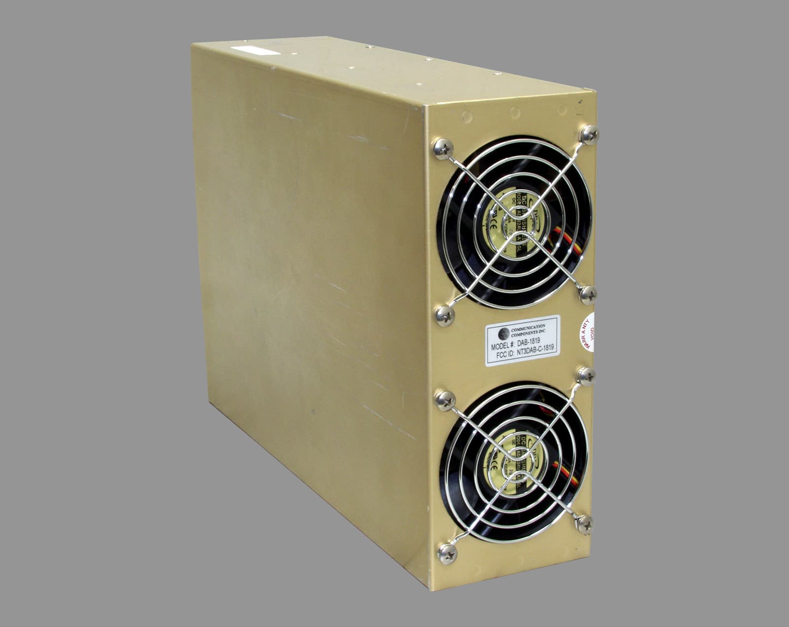
Click to zoom
Application Details
- Equipment Class
- AMP - Amplifier
- Date of Grant
- Jan 22, 2003
- Application Purpose
- Original Equipment
- Date of Application
- Jan 22, 2003
- Equipment Note
- Dual Amplifier Booster
- Frequency Range
- 1930.00000000 - 1990.00000000
- Company
- Communication Components Inc
- Country
- United States
Documents & Files
Document Text
Text extracted from the exhibit documents filed with the FCC. Open a document above to read the original.
Users Manual
GSM Dual Amplifier Booster/ Combiner CCI Model Number DAB-1819 & DAC-1819 USER’S GUIDE Product Description: DAB-1819 & DAC-1819 Dual Amplifier Booster/ Combiner: The CCI GSM Dual Amplifier-Booster Module (DAB) consists of two linear power amplifiers with intermodulation level control circuitry, each capable of generating a 70-75 Watt GSM signal. The Dual Amplifier-Combiner Module (DAC) is identical to the DAB Module with the exception of a passive hybrid combiner at the output which combines both signals to provide two 35-37 Watt GSM signals on a common output. Operation Description: The DAC-1819 and DAB-1819 Dual Amplifier Booster/ Combiner is designed to supply a nominal output power level of 48.5 dBm when used in the uncombined mode. Although the gain of the Dual Amplifier Booster/ Combiner is fixed, the output can be adjusted by setting the input power level. Operation and Installation Instructions: The following instructions should be followed when installing the unit in service: • Apply a 26-28VDC input voltage to the DC Input connector of the Dual Amplifier-Booster/Combiner Module. • Insure that the DC Source is capable of delivering up to 15 Amps at 28VDC. • Apply a GSM signal of up to +41dBm to each RF input port of the Dual Amplifier-Booster/Combiner Module. • The Dual Amplifier-Booster/Combiner Module will provide approximately 7.5dB or less of RF Gain. COMMUNICATION COMPONENTS INC Extending Wireless Coverage 89 Leuning Street Phone: 201-342-3338 2 nd Floor Fax: 201-342-3339 South Hackensack, NJ 07606 www.cciproducts.com z Page 2 • Check the RF output to insure the proper output power is present. {Approximately 70-75 Watts in the uncombined mode (DAB) or 35-37 Watts in the combined mode (DAC)}. • Adjust the input power level to insure the output power level is in compliance with the values indicated in the table on page 2. • Install the Alarm Connector to the Alarm Output connector of the Dual Amplifier-Booster/Combiner Module. Setting the RF Output Power on the DAB & DAC Booster Amplifier The RF output power is not adjustable on the DAB & DAC Booster Amplifier. The user must adjust the RF input power to the Booster Amplifier such that the RF output power level does not exceed the levels shown below in order for the RF output spectral emissions to be compliant with the FCC spurious emissions limit of -13 dBm outside of the assigned frequency block. These levels must not be exceeded. Channel Center Frequency (MHz) Maximum RF 0utput (dBm)* 1930-1930.2 28 1930.2-1989.8 48.8 1989.8-1990 28 *Note: The 28dBm reduced output power will also apply to the first and last channel of any contiguous block of spectrum for any service provider. This equipment complies with Part 24 of the FCC rules. Any changes or modifications not expressly approved by the manufacturer could void the user's authority to operate the equipment. In order to comply with FCC rules for RF exposure, it must be observed that the antenna connected to this equipment be fixed on an outdoor structure and that it must have a minimum separation distance of 10 meters between it and any person."
Cover Letter(s)
REQUEST FOR CONFIDENTIALITY Communication Components Inc. would like to request confidentiality with regard to the following documents in the filing for equipment approval identified by FCC ID. No. NT3DAB-DAC-1819 (1) Schematic diagrams and Parts List contained in electronic file identified as DAB_DAC-1819 Schematics PL.pdf It is the opinion of Communication Components Inc. disclosure of this information would result in significant loss of revenue. This information should be kept confidential for 10 years. Authorized signature: Printed name: Dennis Nathan Company name: Communication Components Inc. Company Address: 89 Leuning Street, South Hackensack, NJ 07606 COMMUNICATION COMPONENTS INC Extending Wireless Coverage 89 Leuning Street Phone: 201-342-3338 2 nd Floor Fax: 201-342-3339 South Hackensack, NJ 07606 www.cciproducts.com
Cover Letter(s)
Barry Quinlan From: "Ruby Dulmage" <[email protected]> To: "Curtis-Straus Certification Dept." <[email protected]> Sent: Friday, December 13, 2002 3:40 PM Attach: DAB_DAC-1819 User's Guide.pdf Sub ject: Re: Communications Components FCC ID: NT3DAB-DAC-1819 Page 1 of 1 1/24/2003 Hi Barry: 1. Regarding the voltage and current for the output stage, the voltage range is 24-30 VDC and the current is 1-6 AMPS. 2. As per section 5 (see summary of test data (note 3)) in the report, the worst case band edge power with margin would be 28dBm (631mW). This only applies to the first and last channel of the frequency block. Attached please find the updated users manual. Thanks, Ruby ----- Original Message ----- From: Curtis -Straus Certification Dept. To: Ruby Dulmage Sent: Friday, December 06, 2002 7:57 PM Subject: Communications Components FCC ID: NT3DAB-DAC-1819 Hi Ruby, The reviewing engineers have identified the following issues: 1. Please supply the DC voltage and current supplied to the final RF stage. 2. We have noted that output power needs to be reduced for the spurious emissions to pass at the bandedges o f each block. What output power is required to achieve this compliance? Also the installation manual needs to reflect that a reduced power is required at the bandedges of each block. Best regards Barry C. Quinlan Certification Manager Curtis-Straus TCB
Operational Description
Tel: 201-342-3338 Fax: 201-342-3339 Email: [email protected] Technical Description General Information CCI’s PCS GSM Cell Booster pro- vides the means to add capacity to existing PCS sites by combining mul- tiple channels onto a common an- tenna port without suffering any com- bining losses. Consequently, capacity of existing sites can be expanded with the existing cabling and antenna infrastructure. The Cell Booster/ Combiner allows the cost efficient implementation of multi-channel high capacity radio networks. The Cell Booster can also be deployed as a booster amplifier without combining, thus increasing the downlink power of the Base Transceiver Station (BTS). When used in conjunction with a Tower Mount Amplifier (TMA), the Cell Booster can significantly in- crease the footprint of rural sites and improve in-building penetration in urban locations. General Info and Technical Description 1 Electrical /Mechanical Specifications 2—3 Mechanical Diagram 4 Contents The PCS Cell Booster was specifically designed to integrate with GSM base stations without any need for retrofitting the original equipment. The system consists of 19” rack mount trays that can accommodate multiple modules. The core modules include a Dual Amplifier-Booster Module and a Dual Amplifier-Combiner Module. The Cell Booster system can be further complemented with a range of Duplexer Modules, Power Supply Modules, and Splitter/VSWR modules. The Cell Booster system can be configured with any combination of the above modules to seamlessly inte- grate with the carriers BTS equipment and achieve the desired performance results. The Dual Amplifier-Booster Module (DAB) consists of two linear power amplifiers with intermodu- lation level control circuitry, each capable of generating a 70 Watt GSM signal. The Dual Ampli- fier-Combiner Module (DAC) is identical to the DAB Module with the exception of a power hybrid combiner at the output which combines both signals to provide two 35 Watt GSM signals on a common output. Both modules incorporate CCI’s proprietary GSM failure-detect circuitry that tracks the amplified GSM signal by timeslot and actively controls and monitors the performance of both amplifiers, providing dry relay contact closures that can be tied into the BTS alarm circuit. Communication Components Inc. PCS GSM Cell Booster/Combiner Model DAB-1819 Model DAC-1819 CCI Confidential Dual Amplifier-Booster (DAB-1819) Module Electrical Specification Operating Frequency: 1930-1990 MHz Rated GSM Output Power: 70 Watts (Per Channel) 1 dB Compression Point: 48.5 dBm Min. Pass Band Ripple: +/-0.5 dB Max. Power Supply Voltage: 28 VDC Nominal Current Consumption: 12 AMPS Typical Dimensions: 8.75”L x 3.5”W x 12”D Number of Inputs/ Outputs: 2 Inputs / 2 Outputs Connectors N or SMA female Weight 13 Lbs. Max. Operating Temperature: -25° to +65° C Ambient Communication Components Inc. Tel: 201-342-3338 Fax: 201-342-3339 Dual Amplifier-Combiner (DAC-1819) Module Electrical Specification Operating Frequency: 1930-1990 MHz Rated GSM Output Power: 35 Watts (Per Channel) 1 dB Compression Point: 45.5 dBm Min. (Per Channel) Pass Band Ripple: +/-0.5 dB Max. Power Supply Voltage: 28 VDC Nominal Current Consumption: 12 AMPS Typical Dimensions: 8.75”L x 3.5”W x 12”D Number of Inputs/ Outputs: 2 Inputs / 1 Outputs Connectors N or SMA female Weight 13 Lbs. Max. Operating Temperature: -25° to +65° C Ambient Communication Components Inc. PCS GSM Cell Booster/Combiner Communication Components Inc. PCS GSM Cell Booster/Combiner Communication Components Inc. Tel: 201-342-3338 Fax: 201-342-3339 89 Leuning Street South Hackensack, NJ 07606 Tel: 201-342-3338 Fax: 201-342-3339 Email: [email protected] W w w . c c i p r o d u c t s . c o m CCI’s Cell Booster/Combiner for PCS Mechanical Drawing Ordering Information Cell Booster 19” Rack Mountable Chassis Cell Booster / Amplifier Plug-in Module Dual Amplifier-Booster Module: CCI Model DAB-1819 Dual Amplifier-Combiner Module: CCI Model DAC-1819 3 . 5 ” 8.75” 1 2 ” 3 . 5 ” 8.75” 1 2 ” 19” 12” 8.75” 19” 12” 8.75”
RF Exposure Info
Exposure of Humans to RF Fields Analysis Performed By: Glen Westwell Date of Test: 14 Nov. 2002 Maximum Permissible Exposure (MPE) Compliance Statement, FCC Radio Frequency Exposure Limit 1.1310 & Industry Canada RSS-102 Communications Components PCS Band Amplifiers DAB-DAC-1819 The DAB-DAC-1819 amplifier has been tested and the performance characterized in accordance with the MPE requirements of FCC 47 CFR and Industry Canada RSS-102. At an operating frequency of 1930-1990MHz the MPE limit for the General Population/Uncontrolled Exposure is 1mW/cm 2 . This device complies with this limit at the following line of sight distances from the antenna element: DAB-DAC-1819 (80W) : 795cm The analysis is provided below. Power Density (S) = EIRP/(4πR 2 ), Therefore, R≥√EIRP/S x 4π Using this calculation: Maximum Antenna Gain (typical installation) = 20dBi Maximum output power (worst case) = 49dBm S = 1.0mW/cm 2 EIRP = 69dBm or 7943.3W(max. worst case) Therefore, R= 795 cm This minimum safe distance for the general population of 10m shall be stated in the installation & operators instruction manual under the RF Safety Exposure Warning Statement. Analysis provided by, Glen Westwell, Nemko Canada Inc. for Communications Componenets.
Test Report
Master: FCC-PR24-E Date: February 13, 2002 Test Report:2W06522.1 Applicant:Communications Components 89 Leuning Street South Hackensack, NJ 07606 U.S.A. Equipment Under Test:PCS BAND, GSM Amplifier FCC ID:NT3DAB-DAC-1819 In Accordance With:FCC Part 24, Subpart E Tested By:Nemko Canada Inc. 303 River Road, R.R. 5 Ottawa, Ontario K1V 1H2 Authorized By: Kevin Carr, EMC Specialist Date:27 November 2002 Total Number of Pages:24 Nemko Canada Inc.FCC PART 24, SUBPART E PROJECT NO.:2W06522.1 EQUIPMENT: PCS BAND, GSM Amplifier Page 2 of 24 Table of Contents Section 1. Summary of Test Results......................................................................................3 Section 2. General Equipment Specification........................................................................5 Section 3. RF Power Output..................................................................................................6 Section 4. Occupied Bandwidth............................................................................................8 Section 5. Spurious Emissions at Antenna Terminals........................................................13 Section 8. Block Diagrams...................................................................................................22 Section 9. Test Equipment List...........................................................................................24 Nemko Canada Inc.FCC PART 24, SUBPART E PROJECT NO.:2W06522.1 EQUIPMENT: PCS BAND, GSM Amplifier Page 3 of 24 Section 1.Summary of Test Results General All measurements are traceable to national standards. These tests were conducted on a sample of the equipment for the purpose of demonstrating compliance with FCC Part 24, Subpart E. THIS TEST REPORT RELATES ONLY TO THE ITEM(S) TESTED. THE FOLLOWING DEVIATIONS FROM, ADDITIONS TO, OR EXCLUSIONS FROM THE TEST SPECIFICATIONS HAVE BEEN MADE. See “ Summary of Test Data”. TESTED BY: ______________________________DATE: 25 November 2002 Glen Westwell, Wireless Technologist Nemko Canada Inc. authorizes the above named company to reproduce this report provided it is reproduced in its entirety and for use by the company’s employees only. Any use which a third party makes of this report, or any reliance on or decisions to be made based on it, are the responsibility of such third parties. Nemko Canada Inc. accepts no responsibility for damages, if any, suffered by any third party as a result of decisions made or actions based on this report. This report applies only to the items tested. Nemko Canada Inc.FCC PART 24, SUBPART E PROJECT NO.:2W06522.1 EQUIPMENT: PCS BAND, GSM Amplifier Page 4 of 24 Summary Of Test Data Name Of TestPara. No.Result RF Power Output2.1046Complies Occupied Bandwidth2.1049Complies Spurious Emissions at Antenna Terminals2.1051Complies Field Strength of Spurious Emissions2.1053Complies Frequency Stability2.1055N/A Notes: (1) This application is for the 80W PCS, GSM inline amplifier. This amplifier is used in the transmit path for a single channel only, and is connected via coaxial connection and operated in an equipment rack at the base station transmitter. (2) This amplifier does not translate the RF input, therefore frequency stability is not applicable. (3) The power levels at the first and last channel of each frequency block must be reduced to achieve compliance. See attached plots in section 5. IndoorTemperature:22 °C Humidity:48 % OutdoorTemperature:7 °C Humidity:52 % Nemko Canada Inc.FCC PART 24, SUBPART E PROJECT NO.:2W06522.1 EQUIPMENT: PCS BAND, GSM Amplifier Page 5 of 24 Section 2.General Equipment Specification Manufacturer: Communications Components Model No.: DAB-1819 DAC-1819 Serial No.: S/N C003929 Date Received In Laboratory: 18 Oct, 2002 Nemko Identification No.: #1 Supply Input Voltage: 120 VAC Frequency Range: Downlink: BLK A: 1930-1945MHz BLK D: 1945-1950MHz BLK B: 1950-1965MHz BLK E: 1965-1970MHz BLK F: 1970-1975MHz BLK C: 1975-1990MHz RF Output (Rated): 80W Amplifier Gain (Rated): 8dB Emission Designator(modulation): GXW Nemko Canada Inc.FCC PART 24, SUBPART E PROJECT NO.:2W06522.1 EQUIPMENT: PCS BAND, GSM Amplifier Page 6 of 24 Section 3.RF Power Output Para. No.: 2.1046 Test Performed By: Glen WestwellDate of Test: 6 Nov 2002 Minimum Standard:Para. No.: 24.232. Test Results:Complies. The maximum RF output power is within ± 1dB of the manufacturer’s rating. This is a base station downlink single channel amplifier only. This result was obtained with an input power of 41.2dBm. Rated Output Power: 49dBm Measured Output Power:48.9dBm Nemko Canada Inc.FCC PART 24, SUBPART E PROJECT NO.:2W06522.1 EQUIPMENT: PCS BAND, GSM Amplifier Page 7 of 24 Nemko Canada Inc.FCC PART 24, SUBPART E PROJECT NO.:2W06522.1 EQUIPMENT: PCS BAND, GSM Amplifier Page 8 of 24 Section 4.Occupied Bandwidth Para. No.: 2.1049 Test Performed By: Glen WestwellDate of Test: 6 Nov 2002 Minimum Standard:Para. No.: 24.238. Test Results:Complies. The occupied bandwidth was measured by comparison of input to the output signal. This was done in order to determine if there was any degradation to the output signal due to the amplification through the repeater. Test Data:See attached graph(s). Nemko Canada Inc.FCC PART 24, SUBPART E PROJECT NO.:2W06522.1 EQUIPMENT: PCS BAND, GSM Amplifier Page 9 of 24 Nemko Canada Inc.FCC PART 24, SUBPART E PROJECT NO.:2W06522.1 EQUIPMENT: PCS BAND, GSM Amplifier Page 10 of 24 Nemko Canada Inc.FCC PART 24, SUBPART E PROJECT NO.:2W06522.1 EQUIPMENT: PCS BAND, GSM Amplifier Page 11 of 24 Nemko Canada Inc.FCC PART 24, SUBPART E PROJECT NO.:2W06522.1 EQUIPMENT: PCS BAND, GSM Amplifier Page 12 of 24 Nemko Canada Inc.FCC PART 24, SUBPART E PROJECT NO.:2W06522.1 EQUIPMENT: PCS BAND, GSM Amplifier Page 13 of 24 Section 5.Spurious Emissions at Antenna Terminals Para. No.: 2.1051 Test Performed By: Glen WestwellDate of Test: 9 Nov 2002 Minimum Standard:Para. No.: 24.238. Test Results:Complies. Note: The power levels at the first and last channel of each…
Text truncated - open the document above for the full version.
Test Setup Photos
Nemko Canada Inc.FCC PART 24, SUBPART E PROJECT NO.:2W06522.1 EQUIPMENT: PCS BAND, GSM Amplifier Page 21 of 24 Radiated Emissions Set-Up Photo Pre-Scan OATS Set-Up
Contact Information
Applicant
Dennis Nathan(President)
Test Firm
Nemko Canada Inc.Stuart Beck
Technical Specifications
| # | Rule Parts | Frequency Range | Power Output | Emission | Tolerance |
|---|---|---|---|---|---|
| 1 | 24 | 1.93 GHz - 1.99 GHz | 80 W | GXW | Amp |
Other Applications from Communication Components Inc
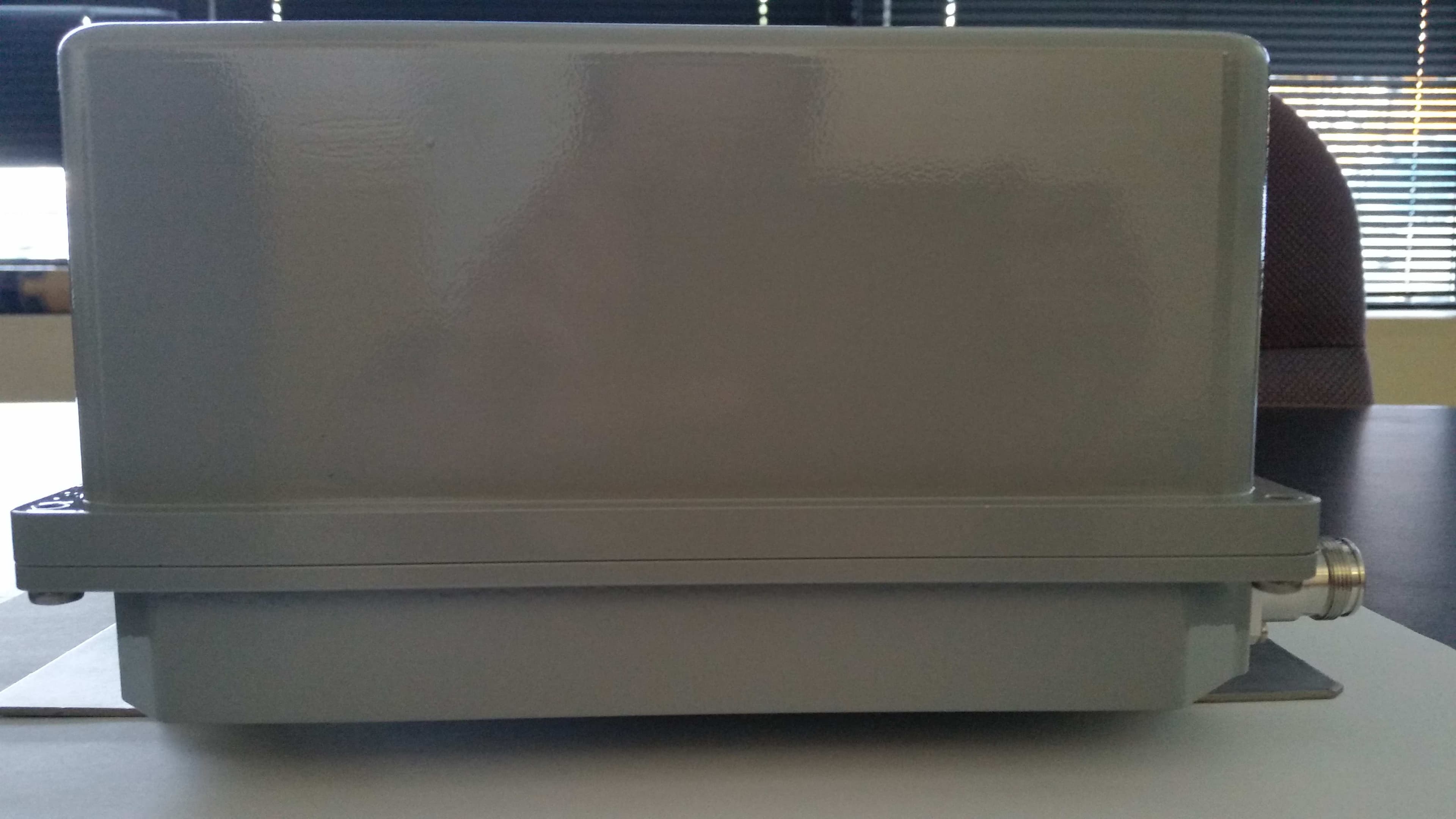
NT3SERRFU8W
Mar 09, 2020SiriusXM SDAR Fiber Repeater
Equipment Class
BOS - All other signal boosters other than 20.21/90.219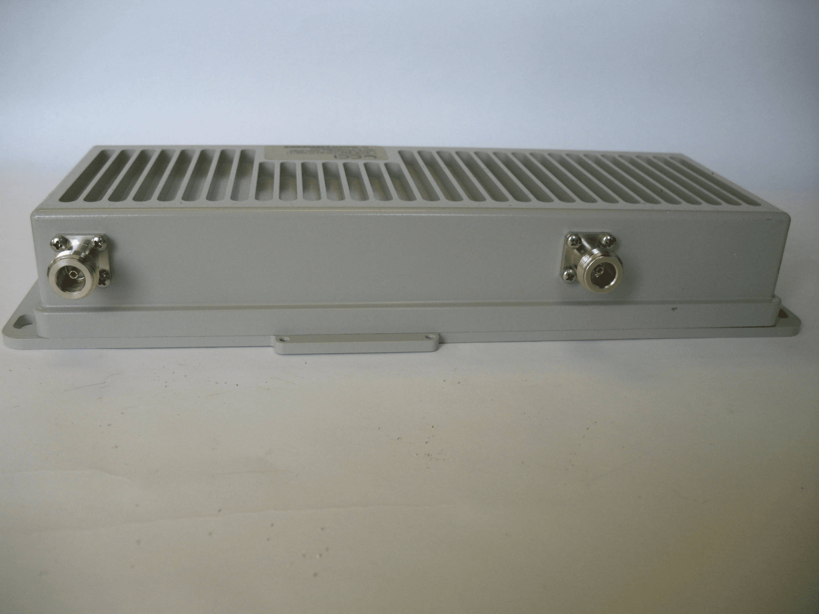
NT3SCB8501WA
Jun 24, 2014Amplifier
Equipment Class
AMP - Amplifier
NT3MCPA2100125
Apr 19, 2011HIGH EFFICIENCY MCPA
Equipment Class
AMP - Amplifier
NT3DAB1819125G2
Jul 28, 2010PCS GSM/EDGE 125W Dual Amplifier Booster
Equipment Class
AMP - Amplifier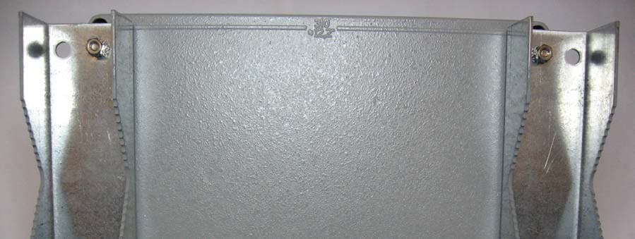
NT3CE-1819-10G2
Jul 03, 2007PCS Multi-Channel Cell Extender
Equipment Class
AMP - Amplifier