NT3DAB-DAC-1819-1PCS Band GSM Amplifer
Communication Components Inc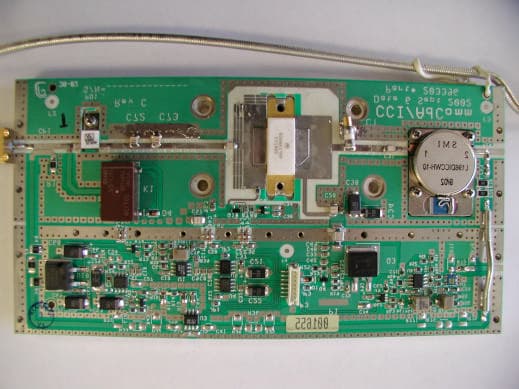
Click to zoom
Application Details
- Equipment Class
- AMP - Amplifier
- Date of Grant
- Dec 08, 2002
- Application Purpose
- Original Equipment
- Date of Application
- Dec 08, 2002
- Equipment Note
- PCS Band GSM Amplifer
- Frequency Range
- 1930.00000000 - 1990.00000000
- Company
- Communication Components Inc
- Country
- United States
Documents & Files
Document Text
Text extracted from the exhibit documents filed with the FCC. Open a document above to read the original.
Users Manual
GSM Dual Amplifier Booster/ Combiner CCI Model Number DAB-1819 & DAC-1819 With Ericsson RBS-2106/2206 GSM Base Transceiver Station USER’S GUIDE Product Description: DAB-1819 & DAC-1819 Dual Amplifier Booster/ Combiner: The CCI GSM Dual Amplifier-Booster Module (DAB) consists of two linear power amplifiers with intermodulation level control circuitry, each capable of generating a 65-70 Watt GSM signal. The Dual Amplifier-Combiner Module (DAC) is identical to the DAB Module with the exception of a passive hybrid combiner at the output which combines both signals to provide two 30-35 Watt GSM signals on a common output. RBS-2106 & RBS-2206 GSM Base Transceiver Station: The Base Transceiver Station (BTS) is a GSM Base Station which serves one cell and is controlled by the Base Station Controller (BSC). The RBS-2106 and RBS 2206 designate the outdoor and indoor versions of the BTS respectively. The BTS contains the radio transceivers and all the digital signal processing equipment. The BTS contains six double Transceiver Radio Unit’s (dTRU’s) for a total of twelve transceivers per BTS. The dTRU consists of two synthesized transmitters (TRX) operating in the frequency band of 1930 to 1990 MHz. There are 299 channels available with a channel spacing of 200 KHz. The transmitter is a constant envelope using 0.3 GMSK modulation, which is MSK filtered with a Gaussian filter, having a BT product of 0.3. The transmitter is capable of operating in a Time Division Multiple Access (TDMA) system. For each channel there are 8 time slots available, each containing digital speech or data. Operation Description: The DAC-1819 and DAB-1819 Dual Amplifier Booster/ Combiner in conjunction with the RBS 2106/2206 BTS are designed to supply a nominal output power level of 47.5 dBm when used in the uncombined mode and 44.5 dBm when used in the combined mode at the antenna connector. A system block diagram is shown on diagram #1 and #2. COMMUNICATION COMPONENTS INC Extending Wireless Coverage 89 Leuning Street Phone: 201-342-3338 2 nd Floor Fax: 201-342-3339 South Hackensack, NJ 07606 www.cciproducts.com z Page 2 COMMUNICATION COMPONENTS INC Extending Wireless Coverage DUPLXR TX1+2/RXA LNA TX3+4/RXB TX1 HC1 TX1+ HC2 TX2 RXA RXB TX 2 dTRU 1 TX1 HC1 TX1+ HC2 TX2 RXA RXB TX 2 dTRU 2 TX1 HC1 TX1+ HC2 TX2 RXA RXB TX 2 dTRU 3 DUPLXR DUPLXR LNA DUPLXR DUPLXR TX9+10/RXB LNA TX11+12/RXA DUPLXR DUPLXR LNA DUPLXR CXU ddTMA ddTMAddTMA ddTMA CXU RBS 2106 BTS DAB-1819 CONFIGURATION CCI Confidential TX CDU-G LNALNA RXARXB DUPLEXERDUPLEXER TXLP TX TXLP 48.5dBm TX CDU-G LNALNA RXARXB DUPLEXERDUPLEXER TXLP TX TXLP 47.5dBm 47.5dBm 41dBm 41dBm 48.5dBm TX CDU-G LNALNA RXBRXA DUPLEXERDUPLEXER TXLP TX TXLP 47.5dBm47.5dBm 41dBm 41dBm DUPLXR TX5+6/RXA LNA TX7+8/RXB DUPLXR DUPLXR LNA DUPLXR ddTMA ddTMA CXU 48.5dBm 41dBm 41dBm 47.5dBm47.5dBm 48.5dBm48.5dBm48.5dBm DIAGRAM 1 DAB- 1819 DAB- 1819 DAB- 1819 COMMUNICATION COMPONENTS INC Extending Wireless Coverage DUPLXR TX1+2/RXA LNA TX3+4/RXB TX1 HC1 TX1+ HC2 TX2 RXA RXB TX 2 dTRU 1 TX1 HC1 TX1+ HC2 TX2 RXA RXB TX 2 dTRU 3 TX1 HC1 TX1+ HC2 TX2 RXA RXB TX 2 dTRU 2 TX1 HC1 TX1+ HC2 TX2 RXA RXB TX 2 dTRU 4 TX1 HC1 TX1+ HC2 TX2 RXA RXB TX 2 dTRU 5 TX1 HC1 TX1+ HC2 TX2 RXA RXB TX 2 dTRU 6 DUPLXR DUPLXR LNA DUPLXR DUPLXR TX9+10/RXB LNA TX11+12/RXA DUPLXR DUPLXR LNA DUPLXR CXU ddTMA ddTMAddTMA ddTMA CXU RBS 2106 BTS DAC-1819 CONFIGURATION CCI Confidential TX CDU-G LNALNA RXARXB DUPLEXERDUPLEXER TXLP TX TXLP DAC- 1819 45.5dBm45.5dBm TX CDU-G LNALNA RXARXB DUPLEXERDUPLEXER TXLP TX TXLP 44.5dBm 44.5dBm 41dBm 41dBm 41dBm 41dBm 45.5dBm45.5dBm TX CDU-G LNALNA RXBRXA DUPLEXERDUPLEXER TXLP TX TXLP 44.5dBm44.5dBm 41dBm 41dBm 41dBm 41dBm DUPLXR TX5+6/RXA LNA TX7+8/RXB DUPLXR DUPLXR LNA DUPLXR ddTMA ddTMA CXU 45.5dBm45.5dBm 41dBm 41dBm 41dBm 41dBm 44.5dBm44.5dBm DIAGRAM 2 DAC- 1819 DAC- 1819 DAC- 1819 DAC- 1819 DAC- 1819 z Page 3 Although the gain of the Dual Amplifier Booster/ Combiner is fixed, the output can be adjusted by setting the input power level. The input to the Dual Amplifier Booster/ Combiner is the Transceiver Radio Unit (TRU) whose output can be set at 16 power levels in 2dB increments. As shown in diagram #1 and #2, setting the output level of the TRU to 41 dBm will result in a power level at the output of the Dual Amplifier Booster/ Combiner of 48.5 dBm in the uncombined mode and 45.5 dBm in the combined mode. The Dual Amplifier Booster/ Combiner is followed by a CDU-G module which contains both a low-pass filter and duplex filter. The low-pass filter secures the required reverse isolation and provides spurious and harmonic suppression of the output signal. The duplex filter allows a single antenna to be used for both transmitting and receiving. Due to the insertion loss of the CDU-G, the maximum output power at the antenna connector of the radio base station is 47.5 dBm in the uncombined mode and 44.5 dBm in the combined mode. Operation and Installation Instructions: The following instructions should be followed when installing the unit in service: • Apply a 26-28VDC input voltage to the DC Input connector of the Dual Amplifier-Booster/Combiner Module. • Insure that the DC Source is capable of delivering up to 15 Amps at 28VDC. • Apply a GSM signal of up to +41dBm to each RF input port of the Dual Amplifier-Booster/Combiner Module. • The Dual Amplifier-Booster/Combiner Module will provide approximately 7.5dB or less of RF Gain. • Check the RF output to insure the proper output power is present. {Approximately 65-70 Watts in the uncombined mode (DAB) or 30-35 Watts in the combined mode (DAC)}. • Adjust the input power level to insure the output power level is in compliance with the values indicated in the table on page 2. • Install the Alarm Connector to the Alarm Output connector of the Dual Amplifier-Booster/Combiner Module. z Page 4 Setting the RF Output Power on the DAB & DAC Booster Amplifier The RF output power is not adjustable on the DAB & DAC Booster Amplifier. The user must adjust the RF …
Text truncated - open the document above for the full version.
Cover Letter(s)
REQUEST FOR CONFIDENTIALITY Communication Components Inc. would like to request confidentiality with regard to the following documents in the filing for equipment approval identified by FCC ID. No. NT3DAB-DAC-1819-1 (1) Schematic diagrams and Parts List contained in electronic file identified as DAB_DAC-1819 sch.pdf and DAB_DAC-1819 bom.pdf It is the opinion of Communication Components Inc. disclosure of this information would result in significant loss of revenue. This information should be kept confidential for 10 years. Authorized signature: Printed name: Dennis Nathan Company name: Communication Components Inc. Company Address: 89 Leuning Street, South Hackensack, NJ 07606 COMMUNICATION COMPONENTS INC Extending Wireless Coverage 89 Leuning Street Phone: 201-342-3338 2 nd Floor Fax: 201-342-3339 South Hackensack, NJ 07606 www.cciproducts.com
Cover Letter(s)
American Telecommunications Certification Body Inc. 6731 Whittier Ave, McLean, VA 22101 December 9, 2002 RE: Communication Components Inc. FCC ID: NT3DAB-DAC-1819-1 I have a few comments on this Application. 1.) Please provide a Form 731 for this Application. 2.) Internal photos show insufficient views. Please re-do all Internal photos, preferably one to a page, of sufficient detail to read the designators on the circuit boards. Please remember to show top and bottom of all photographs. Please show differences between the Amp/Booster and Amp/Combiner products. 3.) External Photos must show front, back, and sides of each unit. 4.) Please separate Parts and Schematics into separate Exhibits. The Exhibit currently uploaded is unsatisfactory. 5.) Please provide plots of BOTH the input and output occupied bandwidth signals fed to this equipment. 6.) Please demonstrate input vs. output power for this device. 7.) Users guide can not be held Confidential. Please review with your client and make changed to the Confidentiality Request letter. 8.) Please provide an operational description with greater detail. The specification literature provided is of insufficient detail. Please refer to Part 2.1033(c) for guidance. Thank you, William H. Graff President and Examining Engineer mailto: [email protected] The items indicated above must be submitted before processing can continue on the above referenced application. Failure to provide the requested information may result in application termination. Correspondence should be considered part of the permanent submission and may be viewed from the Internet after a Grant of Equipment Authorization is issued. Please do not respond to this correspondence using the email reply button. In order for your response to be processed expeditiously, you must submit your documents through the AmericanTCB.com website. Also, please note that partial responses increase processing time and should not be submitted. Any questions about the content of this correspondence should be directed to the sender.
External Photos
DAC1819 - Front View DAB1819 - Front View DAB- 1819 - Top View DAC-1819 - Top View DAB-DAC-1819 - Rear View
External Photos
Amplifier Front Amplifier Rear Amplifier B Front Amplifier B Rear DAB Front View DAB Rear View DAB Side View DAB Top View DAC Front View DAC Rear View DAC Rear View DAC Top View
ID Label/Location Info
FCC PRODUCT LABELING AND WARNING STATEMENT FCC ID Label Specifications: Text is black or white in color and is left justified. Labels are silk-screened and shall be “permanently affixed” at a conspicuous location on the EUT. Proposed Label Location on EUT FCC Warning Statement A FCC Warning Statement is provided in the product manual. FCC ID: NT3DAB-DAC-1819-1
Operational Description
Tel: 201-342-3338 Fax: 201-342-3339 Email: [email protected] Technical Description General Information CCI’s PCS GSM Cell Booster pro- vides the means to add capacity to existing PCS sites by combining mul- tiple channels onto a common an- tenna port without suffering any com- bining losses. Consequently, capacity of existing sites can be expanded with the existing cabling and antenna infrastructure. The Cell Booster/ Combiner allows the cost efficient implementation of multi-channel high capacity radio networks. The Cell Booster can also be deployed as a booster amplifier without combining, thus increasing the downlink power of the Base Transceiver Station (BTS). When used in conjunction with a Tower Mount Amplifier (TMA), the Cell Booster can significantly in- crease the footprint of rural sites and improve in-building penetration in urban locations. General Info and Technical Description 1 Electrical /Mechanical Specifications 2—3 Mechanical Diagram 4 Contents The PCS Cell Booster was specifically designed to integrate with GSM base stations without any need for retrofitting the original equipment. The system consists of 19” rack mount trays that can accommodate multiple modules. The core modules include a Dual Amplifier-Booster Module and a Dual Amplifier-Combiner Module. The Cell Booster system can be further complemented with a range of Duplexer Modules, Power Supply Modules, and Splitter/VSWR modules. The Cell Booster system can be configured with any combination of the above modules to seamlessly inte- grate with the carriers BTS equipment and achieve the desired performance results. The Dual Amplifier-Booster Module (DAB) consists of two linear power amplifiers with intermodu- lation level control circuitry, each capable of generating a 70 Watt GSM signal. The Dual Ampli- fier-Combiner Module (DAC) is identical to the DAB Module with the exception of a power hybrid combiner at the output which combines both signals to provide two 35 Watt GSM signals on a common output. Both modules incorporate CCI’s proprietary GSM failure-detect circuitry that tracks the amplified GSM signal by timeslot and actively controls and monitors the performance of both amplifiers, providing dry relay contact closures that can be tied into the BTS alarm circuit. Communication Components Inc. PCS GSM Cell Booster/Combiner Model DAB-1819 Model DAC-1819 CCI Confidential Dual Amplifier-Booster (DAB-1819) Module Electrical Specification Operating Frequency: 1930-1990 MHz Rated GSM Output Power: 70 Watts (Per Channel) 1 dB Compression Point: 48.5 dBm Min. Pass Band Ripple: +/-0.5 dB Max. Power Supply Voltage: 28 VDC Nominal Current Consumption: 12 AMPS Typical Dimensions: 8.75”L x 3.5”W x 12”D Number of Inputs/ Outputs: 2 Inputs / 2 Outputs Connectors N or SMA female Weight 13 Lbs. Max. Operating Temperature: -25° to +65° C Ambient Communication Components Inc. Tel: 201-342-3338 Fax: 201-342-3339 Dual Amplifier-Combiner (DAC-1819) Module Electrical Specification Operating Frequency: 1930-1990 MHz Rated GSM Output Power: 35 Watts (Per Channel) 1 dB Compression Point: 45.5 dBm Min. (Per Channel) Pass Band Ripple: +/-0.5 dB Max. Power Supply Voltage: 28 VDC Nominal Current Consumption: 12 AMPS Typical Dimensions: 8.75”L x 3.5”W x 12”D Number of Inputs/ Outputs: 2 Inputs / 1 Outputs Connectors N or SMA female Weight 13 Lbs. Max. Operating Temperature: -25° to +65° C Ambient Communication Components Inc. PCS GSM Cell Booster/Combiner Communication Components Inc. PCS GSM Cell Booster/Combiner Communication Components Inc. Tel: 201-342-3338 Fax: 201-342-3339 89 Leuning Street South Hackensack, NJ 07606 Tel: 201-342-3338 Fax: 201-342-3339 Email: [email protected] W w w . c c i p r o d u c t s . c o m CCI’s Cell Booster/Combiner for PCS Mechanical Drawing Ordering Information Cell Booster 19” Rack Mountable Chassis Cell Booster / Amplifier Plug-in Module Dual Amplifier-Booster Module: CCI Model DAB-1819 Dual Amplifier-Combiner Module: CCI Model DAC-1819 3 . 5 ” 8.75” 1 2 ” 3 . 5 ” 8.75” 1 2 ” 19” 12” 8.75” 19” 12” 8.75”
Parts List/Tune Up Info
10/25/02 CCI/AdComm Inc. Page: 1 15:13:22 Bill of Material Parent part: DRASSY203403 Assy,DualAmpBooster,80WattGEN2 Type : A Rev A Level Component Description Qty Required UM T Scrap Seq RtNum Reference Lin ---------- --------------- ------------------------------ ---------------- --- - ------ --- ----- -------------------- --- .1 DRMPEN203088 Enclsr,Dual Amp Bstr&Comb Opt. 1.00 EA R 0.00 0 0 ITEM 2 1 Rev A .1 DRMPCV203089 Cover,DualAmpBster&PwrSupplys 1.00 EA R 0.00 0 0 ITEM 3 2 Rev - .1 DRFNSH203388 Finished Heatsink,DulAmpBstr 1.00 EA M 0.00 0 0 ITEM 4 3 GEN2,Rev - .1 DRSILK203393 Silkscreen,Frt Pnl,DualAmpBstr 1.00 EA M 0.00 0 0 ITEM 6 5 Rev - .1 DRMPRT203389 Isolation Wall,Top & Bottom, 2.00 EA R 0.00 0 0 ITEM 7 6 D.A.B,80Watt-GEN2,Rev A .1 DRMPRT203390 Isolation Wall,Front & Rear, 2.00 EA R 0.00 0 0 ITEM 8 7 Dual Amp Bstr,80Watt,GEN2,Rev- .1 DRMPRT203391 RF Shield,Top,Dual Amp Bstr 1.00 EA R 0.00 0 0 ITEM 10 8 80Watt,GEN2,Rev - .1 DRMPRT203392 RF Shield,Bottom,Dual Amp Bstr 1.00 EA R 0.00 0 0 ITEM 11 9 80Watt,GEN2,Rev - .1 DRASSY203382 Assy,Amp.,80 Watt,Top,GEN 2 1.00 EA A 0.00 0 0 ITEM 12 10 Rev E .1 DRASSY203394 Assy,Amp.,80 Watt,Bottom,GEN 2 1.00 EA A 0.00 0 0 ITEM 13 11 Rev E .1 DRASSY202992 Assy,LED Brd,Cell Bstr/Cmbnr 1.00 EA M 0.00 0 0 ITEM 14 12 Rev - .1 DRASSY203397 Assy,Dual Alrm Brd,D.A.B.GEN 2 1.00 EA M 0.00 0 0 ITEM 15 13 Rev - .1 DRASSY203527 Assy,Front Pallet,DualAmpBstr 1.00 EA A 0.00 0 0 ITEM 16 14 GEN2,Rev - .1 DRCSET203015-2 Cable Set,RF,Dual Amp Combiner 1.00 SET M 0.00 0 0 ITEM 17 15 Rev A .1 DRCABL203017 Cable,Ribbon15PinD,F-15PinConn 1.00 EA R 0.00 0 0 ITEM 18 16 Rev A .1 DRCABL203016 Cable Assy,Ribbon,10Pin-10Pin 1.00 EA R 0.00 0 0 ITEM 19 17 Rev - .1 DRASSY203028 Assy,Fan,Rework Extension,BTS 2.00 EA A 0.00 0 0 ITEM 20 18 Cell Booster,Rev - .1 EN0899FG08 FanGuard,Metal,3 1/8"Fan size 2.00 EA R 0.00 0 0 ITEM 21 19 2.81"Mnt.Hole Ctr,0.195"Thknss .1 MP05008106632A2 Handle,Alu.,Black,0.250 Dia. 1.00 EA R 0.00 0 0 ITEM 22 20 6-32 THD. .1 EN0330B8C102D4 Cap,FeedThru,1000pF,200V,15A 2.00 EA R 0.00 0 0 ITEM 23 21 #8-32 THD,500W .1 DRCSET203019-2 Cable Assy,DC Pwr,DualAmpCombr 1.00 EA R 0.00 0 0 ITEM 24 22 Rev B .1 DRCSET203528 Cable Assy,DualAmpBooster-GEN2 2.00 EA R 0.00 0 0 ITEM 25 23 Rev - .1 CN0100F172117 Conn,N-Type,F,Sm Flg,4 Hole 2.00 EA R 0.00 0 0 ITEM 26 24 .1 CN0802VLP02-1 Conn,Housing,Plug,2-Pin 1.00 EA R 0.00 0 0 ITEM 27 25 VL Series .1 CN1100FSVF81TP2 Terminal,Contact,Socket,12 AWG 2.00 EA R 0.00 0 0 ITEM 28 26 For JST VL Plug .1 HD0404375HC Screw,4-40x3/8",SHCS,S/S 4.00 EA R 0.00 0 0 ITEM 29 27 .1 HD0404250HC Screw,4-40x1/4",CAP,HEX,UNC-3A 4.00 EA R 0.00 0 0 ITEM 30 28 10/25/02 CCI/AdComm Inc. Page: 2 15:13:22 Bill of Material Parent part: DRASSY203403 Assy,DualAmpBooster,80WattGEN2 Type : A Rev A Level Component Description Qty Required UM T Scrap Seq RtNum Reference Lin ---------- --------------- ------------------------------ ---------------- --- - ------ --- ----- -------------------- --- S/S .1 HD0410500PPSMSS Screw,#10x1/2"PH,PAN HD,SM,S/S 8.00 EA R 0.00 0 0 ITEM 31 29 Type B .1 HD0402250PPSS Screw,2-56x1/4"LG,PH PAN,S/S 8.00 EA R 0.00 0 0 ITEM 33 31 UNC-2A .1 HD0406625PPSS Screw,6-32x5/8"PH,PAN HD,S/S 8.00 EA R 0.00 0 0 ITEM 34 32 .1 HD04021125PPSS Screw,2-56x1 1/8",PH PAN,S/S 36.00 EA R 0.00 0 0 ITEM 35 33 .1 HD0604MLKSS Washer,#4,Med.Split Lock S/S 31.00 EA R 0.00 0 0 ITEM 26 34 .1 HD0404250PPSS Screw,4-40x1/4",PH PAN HD,S/S 10.00 EA R 0.00 0 0 ITEM 37 35 .1 HD0404375PPSS Screw,4-40x3/8"PH,Pan Hd,S/S 8.00 EA R 0.00 0 0 ITEM 38 36 .1 HD0404312PF1SS Screw,4-40x5/16"PH,Flat100,S/S 23.00 EA R 0.00 0 0 ITEM 39 37 .1 HD0406312PF1SS Screw,6-32x5/16"PH,Flat100,S/S 2.00 EA R 0.00 0 0 ITEM 40 38 .1 HD0602MLKSS Washer,#2,Med.Split Lock S/S 44.00 EA R 0.00 0 0 ITEM 41 39 .1 HD0606HLKSS Washer,#6,SpltLock,Helical S/S 8.00 EA R 0.00 0 0 ITEM 42 40 .1 HD0408375PPSS Screw,8-32x3/8",PH,PAN HD,S/S 1.00 EA R 0.00 0 0 ITEM 43 41 .1 HD0608SPLKSS Washer,#8,Split Lock,S/S 1.00 EA R 0.00 0 0 ITEM 44 42 .1 HD0404625PPSS Screw,4-40x5/8",PH,PAN HD,S/S 5.00 EA R 0.00 0 0 ITEM 45 43 .1 HD0608281FSS Washer,#8,Flat,0.281 O.D.,S/S 1.00 EA R 0.00 0 0 ITEM 46 44 .1 HD0704HLK Nut,#4-40,HEX,Self-Locking 2.00 EA R 0.00 0 0 ITEM 47 45 .1 HD0604F025SS Washer,#4,Flat 1/4" OD S/S 2.00 EA R 0.00 0 0 ITEM 48 46 .1 HD03004BKE2 Wire,14 AWG Teflon Ins.,Red 0.50 FT R 0.00 0 0 47 19 Strand,M16878/4-B-K-E-2 .1 EN03232200U50 Cap,Electrolytic,2200uF,50V 2.00 EA R 0.00 0 0 ITEM 50 48 Hi-Temp Radial,105C .1 CN140454112 Lug,#2,Terminal,Solder,TinPlat 2.00 EA R 0.00 0 0 ITEM 51 49 .1 HD1401ES221125B Insulation,ShrinkTubing,1/8"BL 0.19 FT R 0.00 0 0 ITEM 52 50 .1 HD1402TFT25020 Insulation,Teflon Tubing,20AWG 0.17 FT R 0.00 0 0 ITEM 53 51 Natural Color .1 HD030020AWGBUSS Wire,20 AWG Buss,CopprTinPlate 0.17 FT R 0.00 0 0 ITEM 54 52 10/25/02 CCI/AdComm Inc. Page: 1 12:38:04 Bill of Material Parent part: DRASSY203527 Assy,Front Pallet,DualAmpBstr Type : A GEN2,Rev - Level Component Description Qty Required UM T Scrap Seq RtNum Reference Lin ---------- --------------- ------------------------------ ---------------- --- - ------ --- ----- -------------------- --- .1 DRMPPT203526 Pallet,Frt,DualAmpBster,GEN2 1.00 EA R 0.00 0 0 C2 1 Rev - .1 DRPCBD203402 PCB,Front Pallet,D.A.B.- GEN 2 1.00 EA M 0.00 0 0 ITEM 3 2 Rev - .1 HD0402250PPSS Screw,2-56x1/4"LG,PH PAN,S/S 24.00 EA R 0.00 0 0 ITEM 4 3 UNC-2A .1 HD0602MLKSS Washer,#2,Med.Split Lock S/S 24.00 EA R 0.00 0 0 ITEM 5 4 .1 ES160618110 Res,Chip,110,2512,5%,1W 4.00 EA R 0.00 0 0 ITEM 11 5 10/25/02 CCI/AdComm Inc. Page: 1 15:22:03 Bill of Material Parent part: DRASSY203404 Assy,DualAmpCombiner80WattGEN2 Type : A Rev A Level Component Description Qty Required UM T Scrap Seq RtNum Reference Lin ---------- --------------- ------------------------------ ---------------- --- - ------ --- ----- -------------------- --- .1 DRMPEN203088 Enclsr,Dual Amp Bstr&Comb Opt. 1.00 EA R 0.00 0 0 ITEM 2 1 Rev A .1 DRMPCV203089 Cover,DualAmpBster&PwrSupplys 1.00 EA R 0.00 0 0 I…
Text truncated - open the document above for the full version.
Test Report
Note: This test report is specially limited to the above client company and the product model only. It may not be duplicated without prior written consent of Bay Area Compliance Laboratory Corporation. This report must not be used by the client to claim product endorsement by NVLAP or any agency of the U.S. Government. FCC PART 24 TYPE APPROVAL EMI MEASUREMENT AND TEST REPORT For Communication Components Inc. 89 Leuning Street 2 nd Floor South Hackensack, NJ 07606 FCC ID: NT3DAB-DAC-1819-1 November 15, 2002 This Report Concerns: Original Report Equipment Type: GSM Amplifier Test Engineer:Benjamin Jing Report No.:R0211011 Test Date:November 1, 2002 Reviewed By:Jeff Lee Prepared By:Bay Area Compliance Laboratory Corporation 230 Commercial Street Sunnyvale, CA 94085 Tel: (408) 732-9162 Fax: (408) 732 9164 Communication Components Inc. FCC ID: NT3DAB-DAC-1819-1 Report # R0211011RptPage 2 of 26FCC Part 24 Type Approval report TABLE OF CONTENTS 1 - GENERAL INFORMATION.................................................................................................................................................4 1.1 PRODUCT DESCRIPTION FOR EQUIPMENT UNDER TEST (EUT).........................................................................................4 1.2 OBJECTIVE................................................................................................................................................................................4 1.3 RELATED SUBMITTAL(S)/GRANT(S)......................................................................................................................................4 1.4 TEST METHODOLOGY.............................................................................................................................................................4 1.5 TEST FACILITY.........................................................................................................................................................................5 1.6 TEST EQUIPMENT LIST............................................................................................................................................................5 1.7 LOCAL SUPPORT EQUIPMENT LIST AND DETAILS...............................................................................................................6 1.8 EXTERNAL I/O CABLING LIST AND DETAILS......................................................................................................................6 2 - SYSTEM TEST CONFIGURATION..................................................................................................................................7 2.1 JUSTIFICATION.........................................................................................................................................................................7 2.2 SCHEMATICS/BLOCK DIAGRAM............................................................................................................................................7 2.3 TEST SETUP BLOCK DIAGRAM..............................................................................................................................................7 2.4 EQUIPMENT MODIFICATIONS.................................................................................................................................................7 3 - SUMMARY OF TEST RESULTS........................................................................................................................................8 4 - RF POWER OUTPUT..............................................................................................................................................................9 4.1 APPLICABLE STANDARD.........................................................................................................................................................9 4.2 TEST PROCEDURE....................................................................................................................................................................9 4.3 TEST EQUIPMENT.....................................................................................................................................................................9 4.4 TEST RESULTS..........................................................................................................................................................................9 5 - EMISSION BANDWIDTH...................................................................................................................................................10 5.1 APPLICABLE STANDARDS.....................................................................................................................................................10 5.2 TEST PROCEDURE..................................................................................................................................................................10 5.3 TEST EQUIPMENT..................................................................................................................................................................10 5.4 PLOTS OF OCCUPIED BANDWIDTH......................................................................................................................................10 6 - OUT OF BAND EMISSIONS AT ANTENNA TERMINALS....................................................................................13 6.1 APPLICABLE STANDARDS.....................................................................................................................................................13 6.2 TEST PROCEDURE..................................................................................................................................................................13 6.3 TEST EQUIPMENT..................................................................................................................................................................13 6.4 T…
Text truncated - open the document above for the full version.
Test Setup Photos
TEST SETUP PHOTOGRAPHS Conducted Emission - Front View Conducted Emission - Rear View Radiated Emission - Front View Radiated Emission - Rear View Base Station Antenna View
Contact Information
Applicant
Dennis Nathan(President)
Technical Contact
Baay Area Compliance LaboratoryJennifer Song
[email protected]201 342 3338
230 Commercial St. · Sunnyvale, California · United States
Test Firm
Bay Area Compliance LaboratoryJohn Chan
Technical Specifications
| # | Rule Parts | Frequency Range | Power Output | Emission |
|---|---|---|---|---|
| 1 | 24 | 1.93 GHz - 1.99 GHz | 35.48 W | AMP |
Other Applications from Communication Components Inc
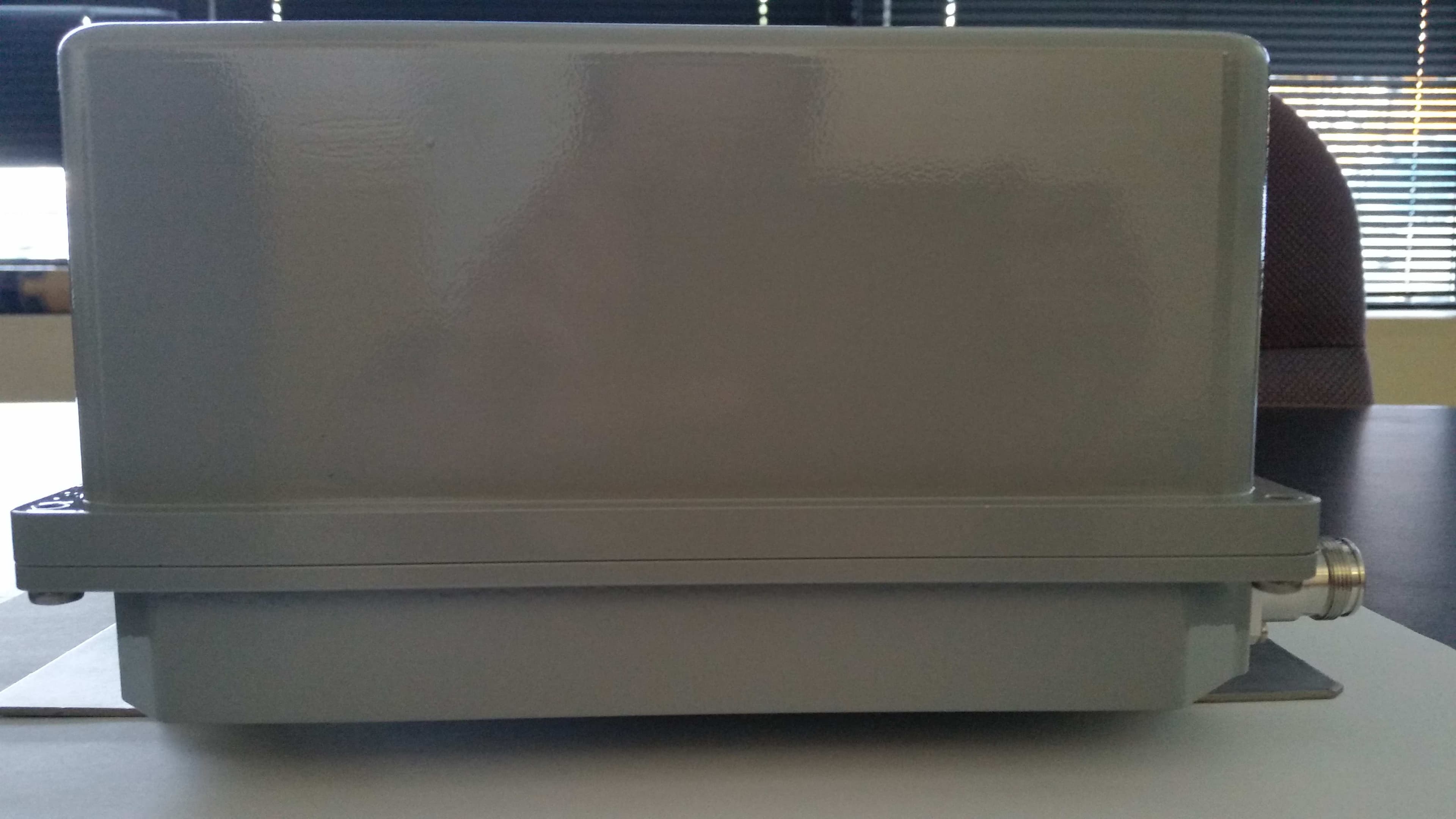
NT3SERRFU8W
Mar 09, 2020SiriusXM SDAR Fiber Repeater
Equipment Class
BOS - All other signal boosters other than 20.21/90.219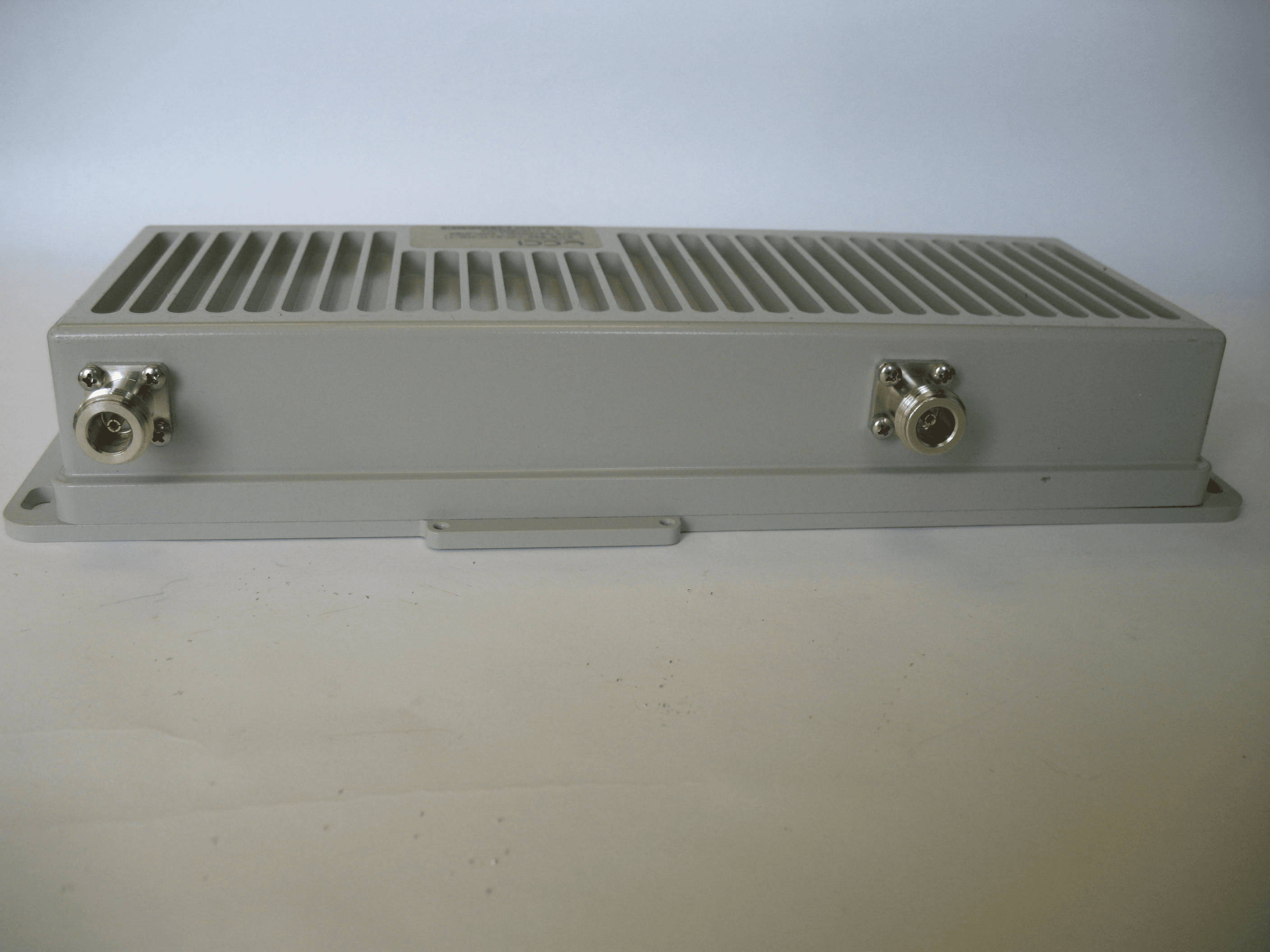
NT3SCB8501WA
Jun 24, 2014Amplifier
Equipment Class
AMP - Amplifier
NT3MCPA2100125
Apr 19, 2011HIGH EFFICIENCY MCPA
Equipment Class
AMP - Amplifier
NT3DAB1819125G2
Jul 28, 2010PCS GSM/EDGE 125W Dual Amplifier Booster
Equipment Class
AMP - Amplifier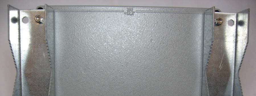
NT3CE-1819-10G2
Jul 03, 2007PCS Multi-Channel Cell Extender
Equipment Class
AMP - Amplifier