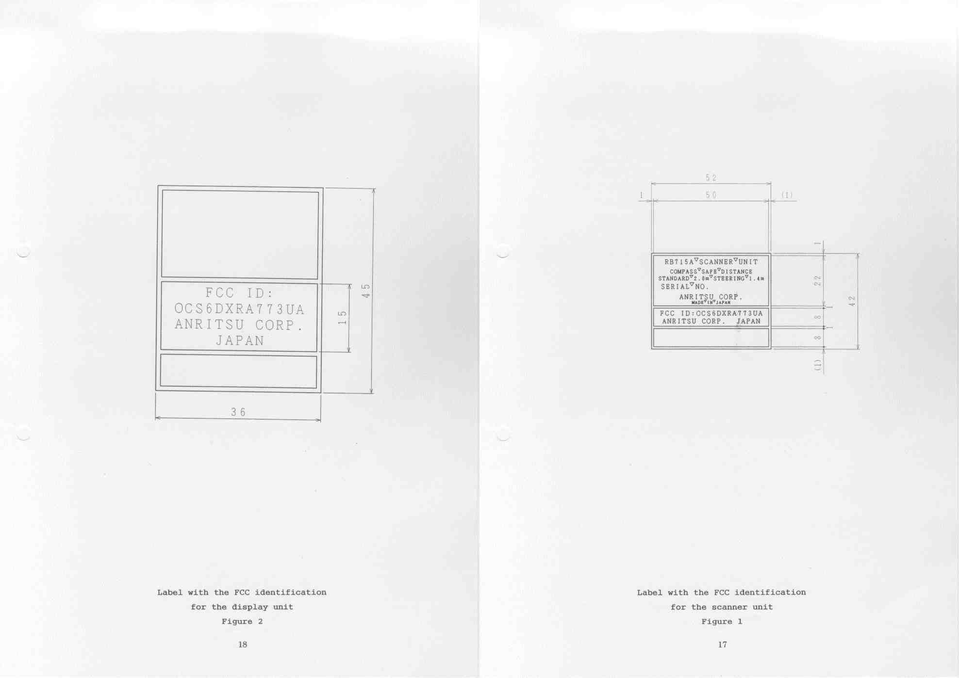
OCS6DXRA773UAMarine Radar RA773UA
Anritsu Corporation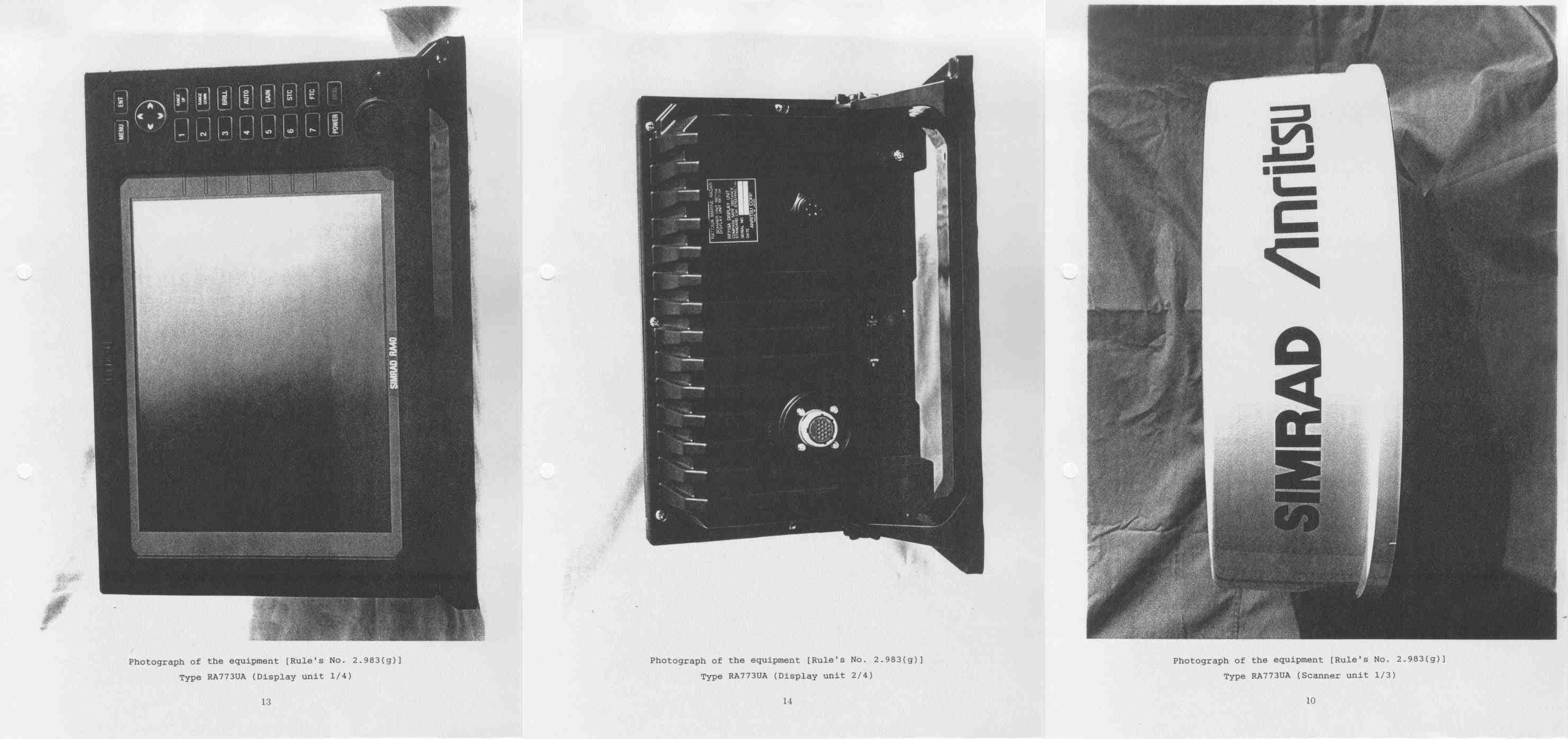
Click to zoom
Application Details
- Equipment Class
- MRD - Marine Radar
- Date of Grant
- Mar 30, 1999
- Application Purpose
- Original Equipment
- Date of Application
- Jan 03, 1999
- Equipment Note
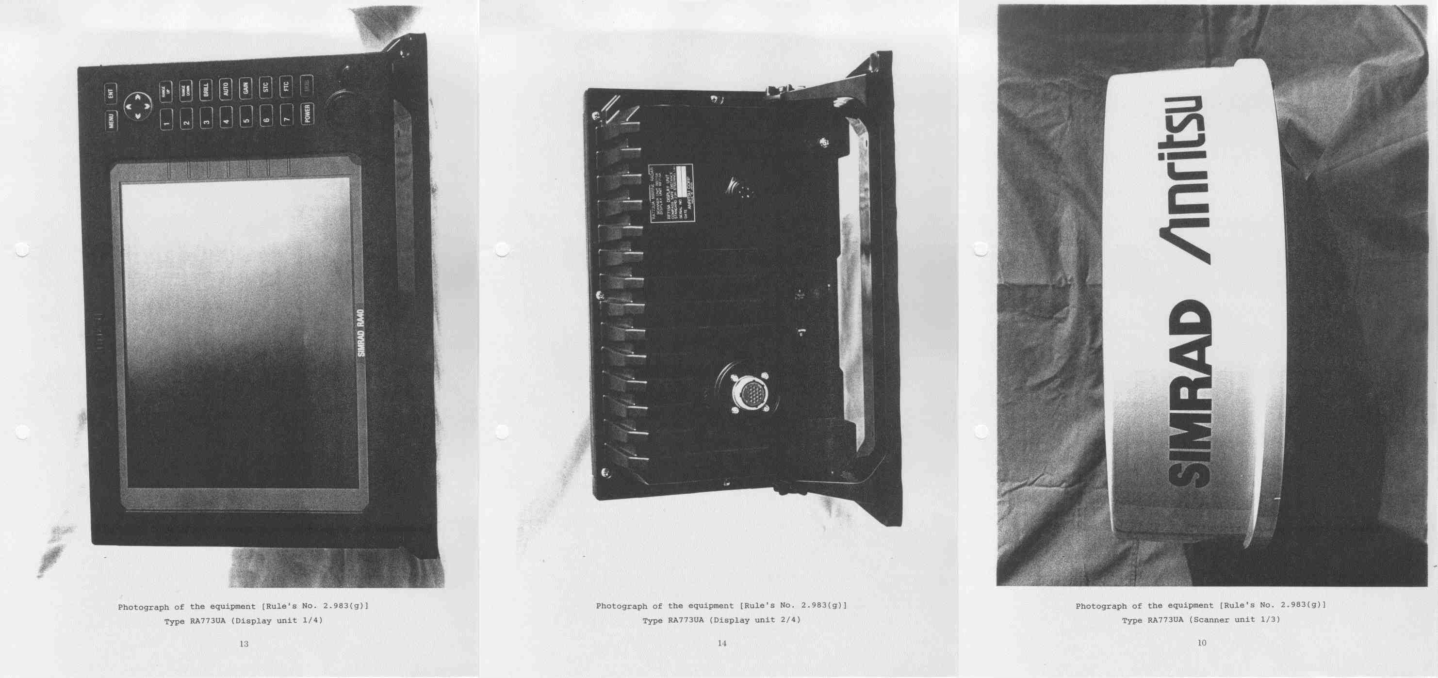
- Marine Radar RA773UA
- Frequency Range
- 9300.00000000 - 9500.00000000
- Company
- Anritsu Corporation
- Country
- Japan
Documents & Files
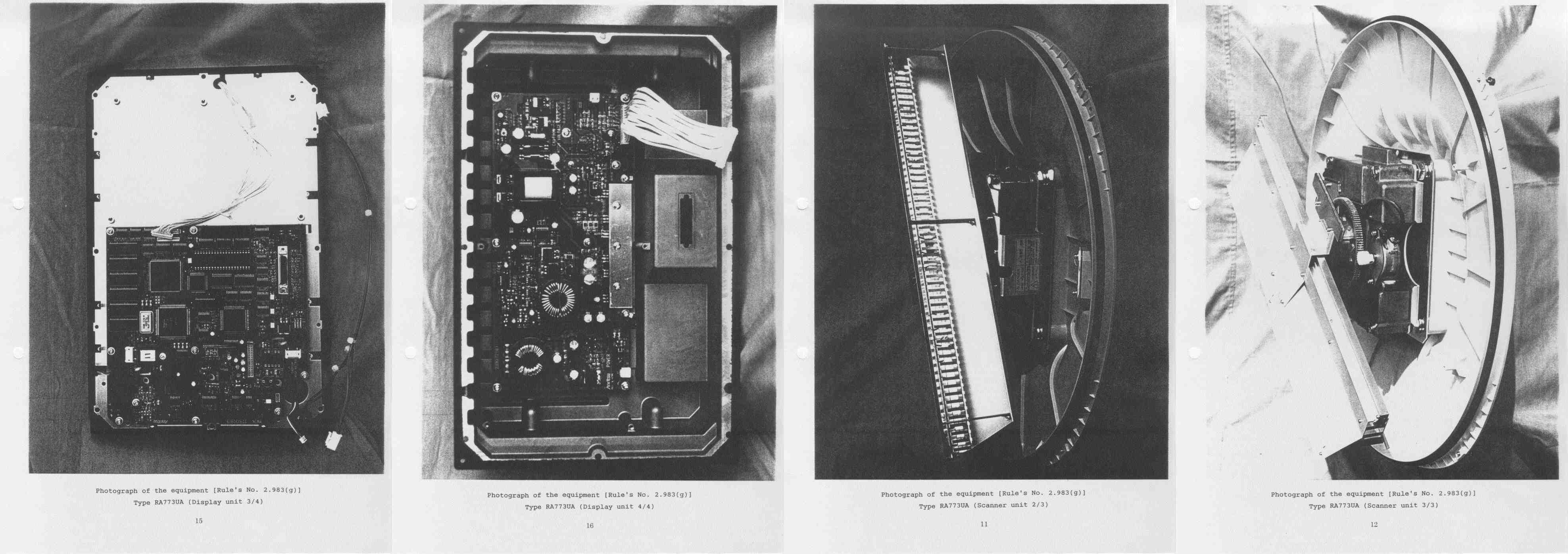
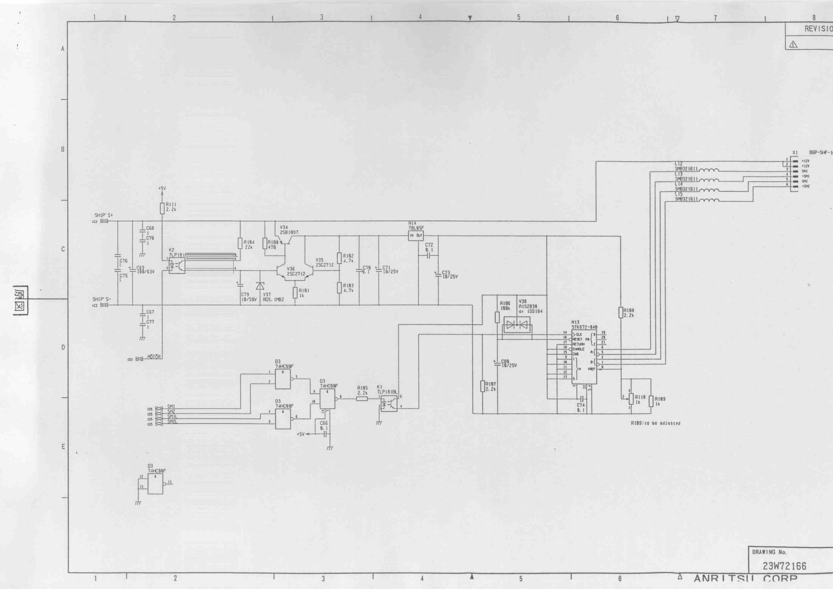
Document Text
Text extracted from the exhibit documents filed with the FCC. Open a document above to read the original.
Operational Description
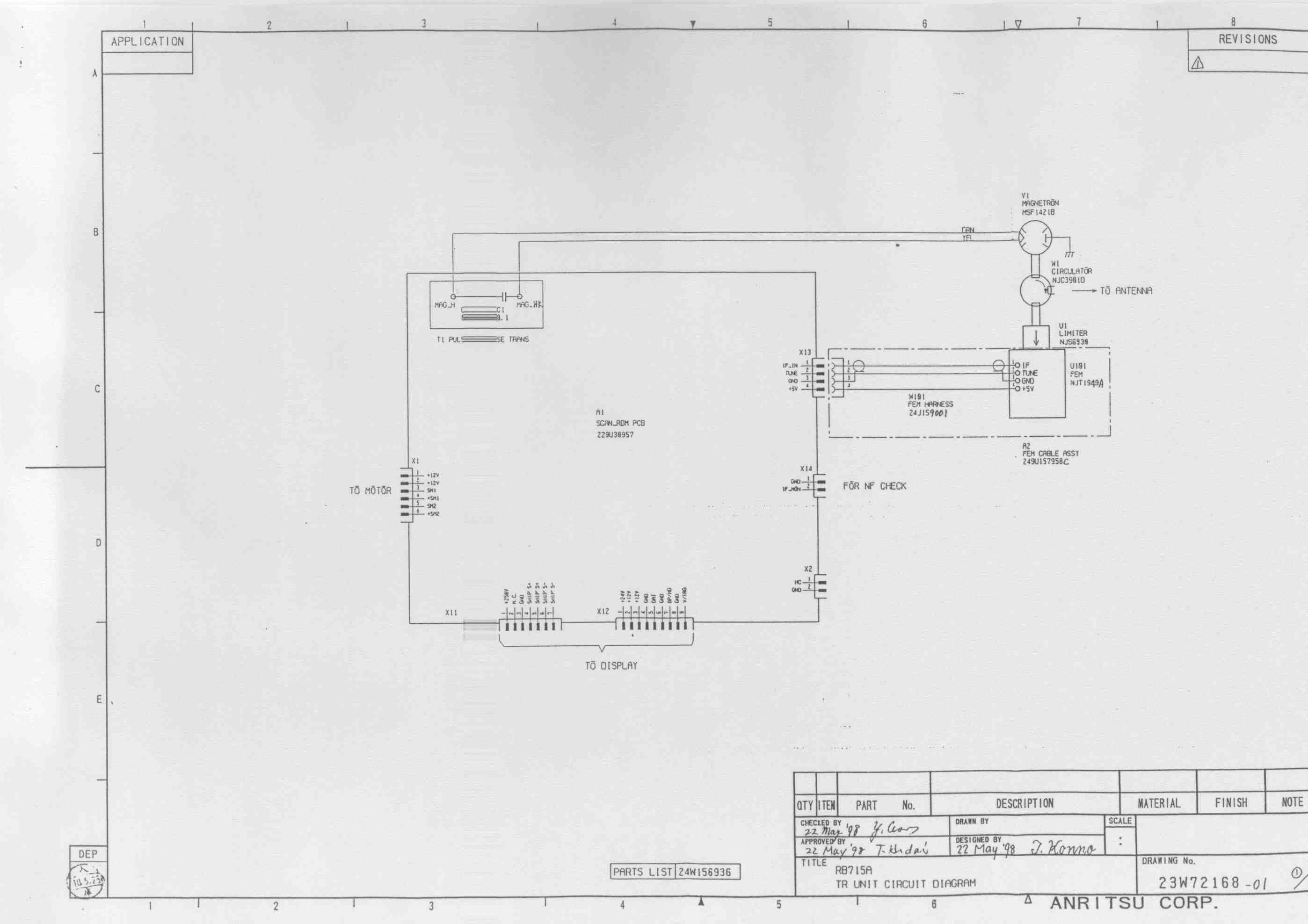
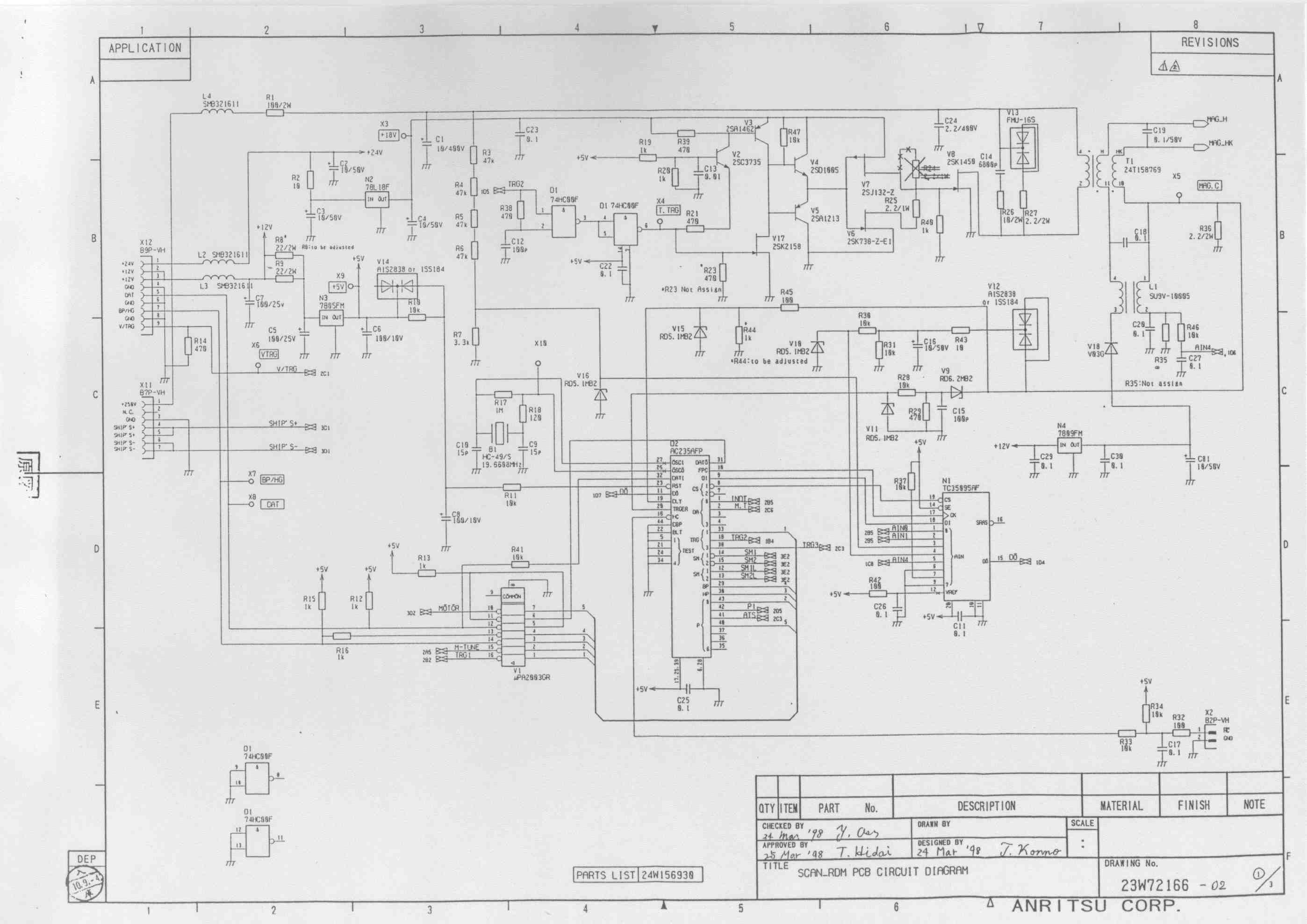
Operational Description MARINE RADAR RA773UA 2 1. A description of all circuitry and devices provided determining and stabilizing frequency. Rule's No. 2.983(d)-(10) 1.1 The oscillating frequency stability of pulsing magnetron depends upon the load characteristics. In this radar, the load of the magnetron consists of a duplexer, a waveguide feeder and an antenna, and the load is matched to the magnetron. The VSWR of the load is better than 1.25 within the specified frequency range. 1.2 Receiver The oscillating frequency stability of FET local oscillator depends upon the supply voltage and ambient temperature. For obtaining the desired frequency stability of oscillator, following means are provided. In addition this radar equips an automatic tuning circuit to coincide the receiver frequency with the transmission frequency. 1.2.1 Temperature compensation High Q strip line of the oscillator circuitry is employed in the Front-End module due to temperature compensation. 1.2.2 Stabilizing the power supply DC voltage supplied to the FET local oscillator is stabilized by the regulator. DC voltage across the varactor diode for tuning is supplied from a D/A converter. The voltage across the D/A converter is made by dividing the regulated 24 volts DC. The regulated voltage is generated by regulator on power supply unit. Therefore stable oscillation can be obtained. 2. A description of any circuits or devices employed for suppression of spurious radiation , for limiting modulation, and for limiting the operating power. Rule's No. 2.983(d)-(11) 2.1 Circuits or devices employed for suppression of spurious radiation. 2.1.1 Suppression of spurious radiation from antenna A duplexer, a waveguide feeder and an antenna perform the narrow band-pass filter and all the spurious signals outside the radar 3 frequency band are suppressed -50dB lower than main radiation level. 2.1.2-1 Line filters The line filters are provided on the ship's power supply line as follows; Line filter L4 and capacitors C1-C4,C18-C19,C68-C69 and C77 on POWER PCB in the display unit. 2.1.2-2 Special interunit connection cable A special 12 cores cable shielded by the metal braid is employed for the interunit connection and the grounding of the braid are made surely at both ends. 2.2 Circuits or devices for limiting the modulation and operating power Transmitting tube, pulsing magnetron, operates with negative going high voltage pulse in the modulator. DC 250 volts as the modulator source generated by the DC-DC converter with voltage regulator(power supply unit) is supplied to the modulator to generate the modulating pulse with constant amplitude. Accordingly, modulation and transmitter power level are maintained constant.
Operational Description
i RA773UA RA774UA Marine Radar Instruction Manual 1st Edition Communication Systems Division Information & Communications Group ANRITSU CORPORATION Document : E-A773/4UA-2-00 i Contents For safety CHAPTER 1 OVERVIEW................................................................................................1 1.1 Introduction ..........................................................................................................................1 1.2 Organization of This Manual ...............................................................................................1 CHAPTER 2 USING RADAR FOR THE FIRST TIME..................................................2 2.1 What is a radar ?...................................................................................................................2 2.2 Characteristics of Radar Wave .............................................................................................3 2.3 Terms Specific to Radars .....................................................................................................6 CHAPTER 3 INSTALLATION ........................................................................................10 3.1 Checking Contents of Your Package....................................................................................10 3.2 Checking Power Supply Voltage .........................................................................................11 3.3 Determining Place of Installation.........................................................................................11 3.3.1 Scanner unit.....................................................................................................................11 3.3.2 Display unit .....................................................................................................................12 3.3.3 Shifting away from obstacles ..........................................................................................13 3.4 Installing Scanner Unit.........................................................................................................14 3.5 Installing Antenna Unit ........................................................................................................16 3.6 Installing Display Unit .........................................................................................................16 3.7 Connecting Cables................................................................................................................17 3.7.1 Interconnecting cable (RA773UA Radome scanner) ......................................................17 3.7.2 Interconnecting cable (RA774UA Open scanner)...........................................................19 3.7.3 Grounding wire ...............................................................................................................20 3.7.4 Power supply cable..........................................................................................................21 3.8 Adjustment ...........................................................................................................................21 3.9 Connecting External Equipment to Display Unit .................................................................22 3.10 When Discarding Your Radar ............................................................................................22 CHAPTER 4 FUNCTIONS AND NAMES ......................................................................24 4.1 Key layout ............................................................................................................................24 4.2 Rear panel ............................................................................................................................25 4.3 Radar screen (Single screen) ................................................................................................25 4.4 Radar screen (Dual screen)...................................................................................................26 4.5 Navigation screen .................................................................................................................26 CHAPTER 5 OPERATION ..............................................................................................28 Basic operation of Radar ............................................................................................................28 5.1 Powering On and Off ...........................................................................................................28 5.2 Adjusting contrast and brilliance of the screen, and key-backlight ......................................28 5.3 Basic Operations ..................................................................................................................29 5.3.1 Powering On and Off ......................................................................................................29 5.3.2 Transmitting ....................................................................................................................29 5.3.3 Adjusting contrast and brilliance of the screen, and key-backlight .................................30 5.3.4 Changing Distance Range (RANGE UP, RANGE DOWN) ...........................................30 5.3.5 Automatic adjustment (AUTO).......................................................................................30 5.3.6 Sensitivity adjustment (GAIN) ........................................................................................ 31 5.3.7 Removing sea clutter (STC) ............................................................................................ 31 5.3.8 Removing rain and snow clutter (FTC) ........................................................................... 32 5.3.9 Man Over Board (MOB) .................................................................................................32 5.4 Functions of Soft Keys ...................................................…
Text truncated - open the document above for the full version.
Parts List/Tune Up Info
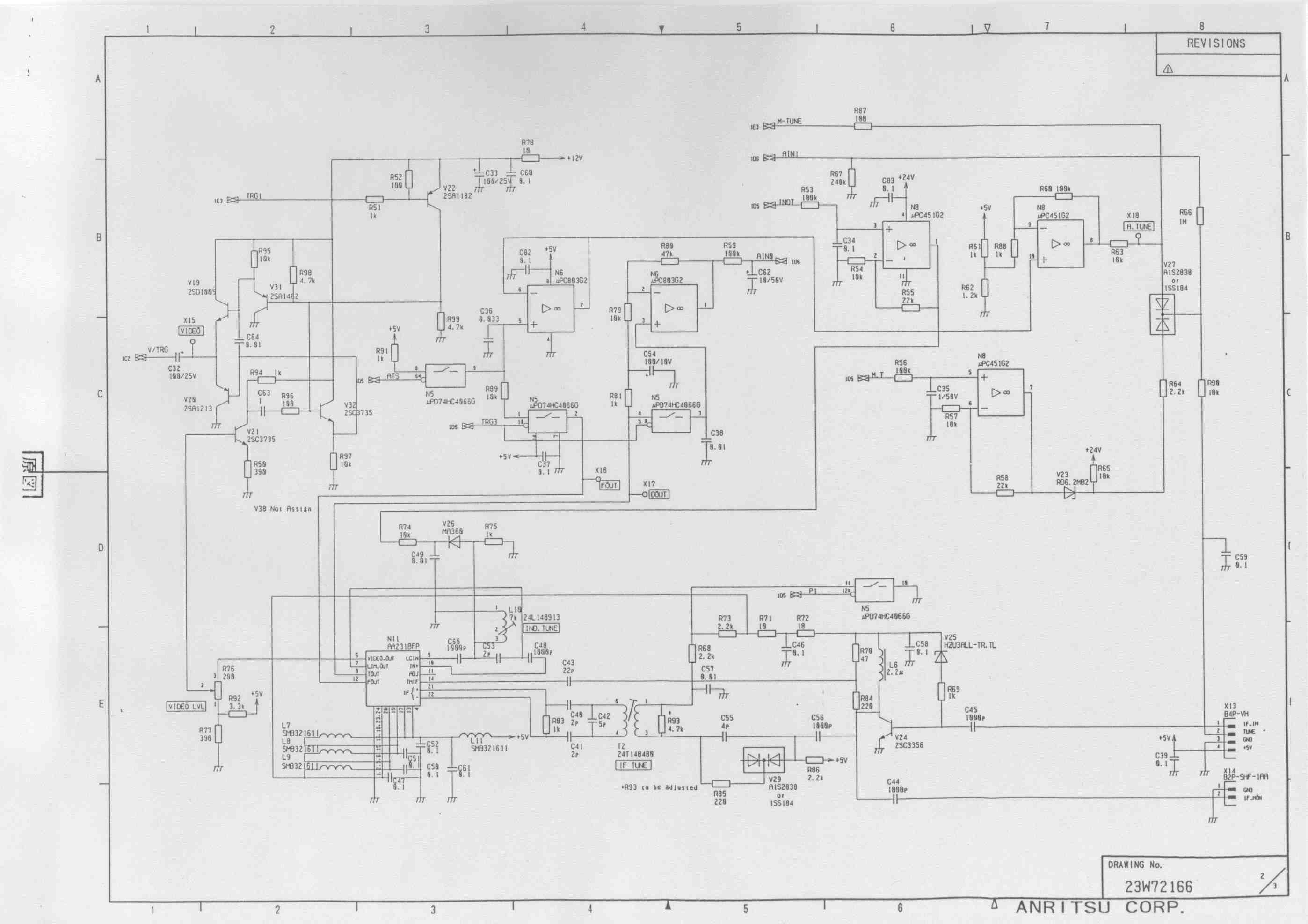
Parts List/Tune Up Info MARINE RADAR RA773UA 2 Technical description that is not described on FCC Form 731 and an attached instruction book for Type RA773UA. 1. Function of each electron tube, semiconductor or other active circuit device Rule's No.2.983 (d) - (6) 1.1 Electron tubes Symbol No.DescriptionTypeFunction V1MagnetronMSF1421BTransmitting tube 1.2 Semiconductor in the chassis of the scanner unit Symbol No.DescriptionTypeFunction U101Front end with X-band amplifier NJT1959RF amplifier, local oscillator and mixer U1Limiter diodeNJS6930Receiver protector at X-band 1.3Semiconductoron SCAN_RDM PCB Symbol No.DescriptionTypeFunction D1,D3IC74HC00FQuadruple 2 input NAND D2ICAC235AFPScanner controller K1,K2Photo couplerTLP181BLIsolator N1ICTC35095AF8ch A/D converter N2IC78L18FVoltage regulator N3IC7805FMVoltage regulator N4IC7809FMVoltage regulator N5ICuPD74HC4066 G Analog switch N6ICuPC803G2Dual Op-amp N8ICuPC451G2Dual Op-amp N11ICAA231BFPLogarithmic amplifier N13ICSTK672-040Motor driver 3 N14IC78L15FVoltage regulator Symbol No.DescriptionTypeFunction V1ICuPA2003GRTransistor array V2,V21,V32Transistor2SC3735Buffer amplifier V3,V31Transistor2SA1462Pulse amplifier V4Transistor2SD1005Switching high voltage V5Transistor2SA1213Switching high voltage V6FET2SK738-Z-E1Switching high voltage V7FET2SJ132-ZSwitching high voltage V8FET2SK1450Switching high voltage V9,V23Zener diodeRD6.2MB2Rectifier for magnetron current V10-V11,V15Zener diodeRD5.1MB2Rectifier for magnetron current V12,V27DiodeA1S2838Rectifier for magnetron current V13DiodeFMU-16SDamping diode V14DiodeA1S2838Switching diode V16,V37Zener diodeRD5.1MB2Limiter V17FET2SK2158Pulse Amplifier V18DiodeV03GRectifier for magnetron current V19Transistor2SD1005Output buffer for video V20Transistor2SA1213Output buffer for video V22Transistor2SA1182Amplifier V24Transistor2SC3356Pre-amplifier V25Zener diodeHZU3ALL- TR,TL Limiter V26DiodeMA360Temperature compensator V29DiodeA1S2838Switching of band width V34Transistor2SB1097Voltage regulator V35-V36Transistor2SC2712Differential amplifier V38DiodeA1S2838Switching diode 4 1.4 Semiconductor in the chassis of the display unit Symbol No.DescriptionTypeFunction H1LCD moduleLM64P302LCD display U1EncoderRECW20D-50- 201-1D Encoder 1.5 Semiconductor of MAIN PCB Symbol No.DescriptionTypeFunction D1-D2,D24,D26IC74HC541FOctal 3-state buffer D3ICAC233CFPGraphic memory controller D4ICuPD72020GC- 8-3B6 Graphic controller D5-D8,D13-D14ICVRAM2M70J256kX8 VRAM D9-D12IC74HC166F8-bit shift register D15ICSRAM32KX8- 12CF 32kX8 SRAM D16ICHD6413003TF1 6 16bit CPU D17-D18IC74HC138FDecoder D19,D28IC74HC273FOctal D-flip-flop D20ICEPROM256kX1 6-12C 256kX16 EPROM D21IC24LC04B/SN512kX8FRAM D22IC74HC74FDual D-flip-flop D23,D39IC74HC14FSchmitt-trigger inverter D25,D33IC74HC245FOctal bus transceivers D27IC74HC05FHex. Inverter D29-D30IC74HC595F8-bit shift register D31ICMB89251A-PFSerial data transmitter/Receiver D32IC74HC123FDual Multivibrators D34ICTC35095AF8ch A/D converter Symbol No.DescriptionTypeFunction 5 D35ICAC232CFPVideo signal processor D36ICHM62832HJP- 25 32kX8 SRAM D37ICMC14046BFPhase locked loop D38ICuPD485505G- 25 Line buffer D40IC74HC74FDual D-flip-flop K1-2,4-6Photo couplerTLP181BLIsolator K3Photo couplerPC356TIsolator N1ICTL7759CPSVoltage detector N2-5ICTHS124Hole IC N6,N9ICuPC451G2Quadruple Op-amp N7IC78L05FVoltage regulator N8ICMB88346BPF12ch 8bit D/A converter N10ICAA239BFPVideo controller V1FET2SK1419Switch V2Thyristor03P2JOver current protector V3Zener diodeRD10MB2Voltage regulator V4DiodeDF10LC20UVoltage protector V5,V36TransistorUN211FBuffer amplifier V6-V7,V39- V40,V43 Diode1SS123Switching diode V8,V10- V11,V17- V18,V25 Diode1SS184Switching diode V9,V34TransistoruPA2003GRTransistor array V12Zener diodeRD5.1MB2Voltage regulator V13,V19,V22,V2 6,V38,V42 TransistorUN221LBuffer amplifier V14Transistor2SA1213CFL amplifier V15-V16Transistor2SD1000CFL amplifier V20-V21Transistor2SC2712Buffer amplifier 6 Symbol No.DescriptionTypeFunction V23,V27-V33LEDTLG260Illuminator V24Transistor2SA1213Buffer amplifier V35Transistor2SD1000Trigger amplifier V37Transistor2SB799Output buffer for video V41FET2SK2158Switch 1.6 Semiconductor of POWER PCB Symbol No.DescriptionTypeFunction D1ICTC4011BF(N)Quadruple 2 input NAND K1Photo couplerTLP181BLIsolator K2Photo couplerPC356TIsolator N1-2ICuPC494GSwitching controller N3ICuPC1093TVoltage regulator V1Transistor2SC2873Voltage regulator V2,V19-V20,Transistor2SC2712Buffer amplifier V3,V8DiodeDE5SC6M- 4061 Rectifier V4-V5DiodeD1FL20U-4063Rectifier V6-V7DiodeRU4ARectifier V9,V11Zener diodeRD20MB2Voltage protector V10Zener diodeRD10MB2Voltage regulator V12,V14,V17,V2 2 Transistor2SA1213Buffer amplifier V13,V15,V18,V2 6 DiodeD1FS4-4063Switching diode V16,V25,V28FET2SK1419Switch V21Transistor2SC2873Buffer amplifier V23-V24FET2SK2010Switch V27Transistor2SA1162Switch V29Transistor2SB1097Voltage regulator 7 V30-V31Transistor2SC2712Voltage regulator Symbol No.DescriptionTypeFunction V32,V42Zener diodeRD5.1MB2Voltage regulator V33TransistorUN221LBuffer amplifier V34-V36DiodeDF10LC20U- 4062 Voltage protector V37Transistor2SC3631-ZSwitch of H.T. V38TransistorUN2113Buffer amplifier V39DiodeA1SS123Switching diode V40Transistor2SA1413-ZSwitch of H.T. V41Transistor2SA1213Switch of H.T. 8 2. Tune up procedure over the power range or at specific operating power levels. Rule's No. 2.983(d)-(9) 2.1 Transmitter Pulse radars employ a pulse-excited magnetron as the transmitter tube. The magnetron used in this radar has a fixed cavity resonator which determines the oscillating frequency. Accordingly, this radar transmitter has no more frequency-adjust circuitry. 2.2 Receiver Pulse radars receive the reflected signal from targets, therefor receiving signal has the same frequency as the transmitter power output. Thus, the radar receiver is tuned to the transmitting frequency. This radar has a super heterodyne type receiver with a Front-End module. The Front-End module consists of a GaAs FET low noise amplifier, a do…
Text truncated - open the document above for the full version.
Test Report
TEST REPORT MARINE RADAR RA773UA 2 Foreword The following information is being submitted in compliance with paragraphs 2.983, 2.985, 2.987, 2.989, 2.991, 2.993 and 2.995 as provided by part 83 of the FCC Rules and Regulations for Type Acceptance of the Anritsu Marine Radar, Type RA773UA. All testing was performed by the Anritsu Corporation Atsugi Factory, 1800, Onna, Atsugi-shi, Kanagawa 243-8555, Japan. 3 STANDARD TEST CONDITIONS and ENGINEERING PRACTICES Except as noted herein, the following conditions and procedure were observed during the testing: ROOM TEMPERATURE =255 ROOM HUMIDITY =20-50% Prior to testing, the E.U.T. was tuned up in accordance with the manufacturer's alignment procedures. All external gain controls were maintained at the position of maximum and/or optimum gain throughout the testing. MEASUREMENT DATA, unless otherwise noted, are WORST CASE measurements. 4 Table of contents Data for the acceptance of the Anritsu Marine Radar Type RA773UA List of Exhibit Exhibit Number 1 RF Power Output (2.985) 2 Modulation Characteristics (2.987) 3 Occupied Bandwidth (2.989) 4 Spurious Emissions at Antenna Terminal (2.991) 5 Spurious Emissions Field Strength (2.993) 6 Frequency Stability (2.995) 5 Exhibit 1 RF POWER OUTPUT (2.985) Type of Transmission: P0N Type of Modulation: Pulse Frequency Band: 9410 MHz 30 MHz Frequency Source: Fixed Cavity Resonator Pulse Rate: 600 Hz to 2000 Hz, Selectable as a function of Range Pulse Width: 0.11 us to 0.8 us, Selectable as a function of Range TEST EQUIPMENT Equipment ManufacturerModel 1. X-Band Directional Coupler Hewlett-Packard X752D 2. Variable Attenuator Hewlett-Packard X382A 3. Power Meter ANRITSU ML83A 4. Crystal Detector Hewlett-Packard 423B 5. Oscilloscope TEKTRONIX 2445 6. Frequency meter Hewlett-Packard X532B 7. X-Band Dummy Load NIHON KOSHUHA WDL095 TEST PROCEDURE The Marine Radar is capable of generating the following pulses: 110ns 2000Hz, 250ns 1500Hz, 0.8 600Hz The Power output for each of these combinations was measured by using the following procedure: (1) Set up the equipment as shown in Fig.1. (2) Record reading of Power Meter. (3) Calculate mean power according to attenuation. (4) Measure and record pulse width and P.R.F. by using oscilloscope and frequency counter. (5) Calculate peak power as follows: P0=Pm/(FrxT) P0:PeakPower,Pm:MeanPower,Fr:P.R.F.* T : Pulse Width, * P.R.F. : Pulse Repetition Frequency 6 7 Exhibit 1 TEST RESULT Transmit Pulse width and P.R.F. Measured Mean Power Measured Pulse width Measured P.R.F. Calculated Peak power Output 110ns2000Hz 0.97W 124.0nS 2008Hz 3.90kW 250ns1500Hz1.53W243.7nS1473Hz4.26kW 800ns600Hz2.02W773.0nS583Hz4.48kW 8 Exhibit 2 MODULATION CHARACTERISITICS (2.987) Type of Transmission: P0N Type of Modulation: Pulse Frequency Band: 9410 MHz 30MHz Frequency Source: Fixed Cavity Resonator Pulse Rate: 600 to 2000 Hz, Selectable as a function of Range Pulse Width: 0.11 us to 0.8 us, Selectable as a function of Range TEST EQUIPMENT Equipment ManufacturerModel 1. X-Band Directional Coupler Hewlett-Packard X752D 2. Variable Attenuator Hewlett-Packard X382A 3. Power Meter ANRITSU ML83A 4. Crystal Detector Hewlett-Packard 423B 5. Oscilloscope TEKTRONIX 2445 6. Frequency meter Hewlett-Packard X532B 7. X-Band Dummy Load NIHON KOSHUHA WDL095 TEST PROCEDURER The Marine Radar is capable of generating the following pulses: 0.11usx2000Hz,0.25usx1500Hz,0.8usx600Hz The Modulation characteristics for each of these combinations was measured by using the following procedure: (1) Set up the equipment as shown in Fig.1. (2) Obtain a convenient display on the oscilloscope and adjust peak to the suitable cursor line. (3) Decrease variable attenuator 3 dB, and measure the pulse width at the cursor line. (4) Photograph the oscilloscope display. (5) Note and record the Frequency Readout of the counter as "Pulse Repetition Frequency". 9 Exhibit 2 TEST RESULT Modulation Characteristics (Detected Pulse) (1) Short Pulse Pulse width (-3 dB) = 124 ns Pulse repetition Frequency = 2008 Hz 50 ns/div. 10 Exhibit 2 TEST RESULT Modulation Characteristics (Detected Pulse) (2) Middle Pulse Pulse width (-3 dB) = 244 ns Pulse repetition Frequency = 1473 Hz 50 ns/div. 11 Exhibit 2 TEST RESULT Modulation Characteristics (Detected Pulse) (3) Long Pulse Pulse width (-3 dB) = 773 ns Pulse repetition Frequency = 583 Hz 100 ns/div. 12 Exhibit 3 OCCUPIED BANDWIDTH (2.989) Type of Transmission: P0N Type of Modulation: Pulse Frequency Band: 9410 MHz 30 MHz Frequency Source: Fixed Cavity Resonator Pulse Rate: 600 to 2000 Hz, Selectable as a function of Range Pulse Width: 0.11 us to 0.8 us, Selectable as a function of Range TEST EQUIPMENT Equipment ManufacturerModel 1. X-Band Directional Coupler Hewlett-Packard X752D 2. Variable Attenuator Hewlett-Packard X382A 3. X-Band Dummy Load NIHON KOSHUHA WDL095 4. Spectrum Analyzer Anritsu MS710C TEST PROCEDURE The Marine Radar is capable of generating the following pulses: 110 ns 2000 Hz, 250 ns 1500 Hz, 800 ns 600 Hz The occupied bandwidth for each of these combinations was measured by using the following procedure: (1) Connect the equipment as shown in Fig.3. (2) Adjust center frequency, span reference level of spectrum analyzer and attenuator if necessary, such that the display nearly fills the screen. (3) Measure and record spectrum and bandwidth The bandwidth is calculated so that the total powers lower than the lowest frequency in the bandwidth and higher than the highest frequency in the bandwidth occupy 0.5% of the transmitted total power respectively. 13 14 Exhibit 3 TEST RESULT Transmission Spectrum of 110 ns 2000 Hz Center frequency : 9.4179GHz Frequency span : 20.0 MHz/div. Level : 10 dB/div. Resolution band width : 300 kHz/div. Video band width : 1 MHz/div. Sweep time : 200 msec/div. Occupied band width : 54.4 MHz 15 Exhibit 3 TEST RESULT Transmission Spectrum of 250 ns 1500 Hz Center frequency : 9.4179GHz Frequency span : 10.0 MHz/div. Level : 10 dB/div. Resolution band width : 300 kHz/d…
Text truncated - open the document above for the full version.
Contact Information
Applicant
Yasuyuki Oishi(R&D Engineer)
Technical Contact
Anritsu Corporation, Atsugi FactoryYuji Sekine
[email protected]+81-462-96-6592
1800, Onna, Atsugi-shi, Kanagawa · Japan
Non-Technical Contact
Anritsu Corporation, Americas DivisionHiroshi Miki
[email protected]+81-3-3473-7203
Technical Specifications
| # | Rule Parts | Frequency Range | Power Output | Emission |
|---|---|---|---|---|
| 1 | 80 | 9.30 GHz - 9.50 GHz | 4000 W | 27M0PON |
Other Applications from Anritsu Corporation
OCS-MT1100A
Oct 08, 2014Network Master Flex
Equipment Class
DSS - Part 15 Spread Spectrum Transmitter
OCS-MT1000A
Jun 24, 2014Network Master Pro
Equipment Class
DSS - Part 15 Spread Spectrum Transmitter
OCS6DXRA775UA
Feb 22, 2000Marine Radar RA775UA
Equipment Class
MRD - Marine Radar
OCS6DXRA774UA
Apr 28, 1999Marine Radar RA774UA
Equipment Class
MRD - Marine Radar