OK8IBM38502.4 GHz Cordless Phone
Shenzhen Baoan Hantong Electronics Factory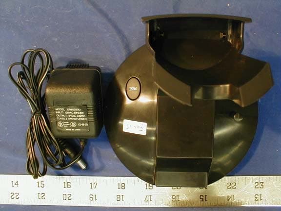
Click to zoom
Application Details
- Equipment Class
- DXX - Part 15 Low Power Communication Device Transmitter
- Date of Grant
- Nov 11, 2001
- Application Purpose
- Original Equipment
- Date of Application
- Nov 11, 2001
- Equipment Note
- 2.4 GHz Cordless Phone
- Frequency Range
- 2472.21000000 - 2476.94000000
- Country
- China
Documents & Files
Document Text
Text extracted from the exhibit documents filed with the FCC. Open a document above to read the original.
Users Manual
1 OPERATION MANUAL FOR IBM 3850 DRAFT 2 Table of Contents The Handset and Base Unit Drawing....................................................................................................................3 A.The Standby Display...................................................................................................................4 B.Cordless Telephone Operation.......................................................................................................5 B.1Preparing for Use..............................................................................................................5 B.2Receiving Calls..................................................................................................................5 B.3Placing Calls......................................................................................................................5 B.4Extension Phones.............................................................................................................6 B.5Using the Headset Feature.............................................................................................................6 B.6Redial Feature...............................................................................................................................6 B.7Out of Range Warning....................................................................................................................6 B.8Handset Paging............................................................................................................................6 C.Caller ID System.....................................................................................................................................7 C.1Viewing Caller Information During Incoming Calls..............................................................................7 C.2“MSG WAITING” (Message Waiting)...............................................................................................7 C.3Call Waiting..................................................................................................................................8 C.4Voice Mail Function.......................................................................................................................8 C.5“C-F” (Forwarded Call)....................................................................................................................8 C.6“L-D-C” (Long Distance Call)...........................................................................................................8 C.7Caller List.....................................................................................................................................8 C.7.1Viewing the Caller List.............................................................................................................9 C.7.2Placing a Call from the Caller List..............................................................................................9 C.7.3Saving the Name and Number in the Caller List into the DIRECTORY............................................9 C.7.4Deleting All Records in the Caller List........................................................................................9 C.7.5Selective Deleting in the Caller List...........................................................................................9 C.8Name and Telephone Number DIRECTORY.....................................................................................10 C.8.1Viewing the DIRECTORY.........................................................................................................10 C.8.2Speed Viewing the DIRECTORY...............................................................................................10 C.8.3Saving in the DIRECTORY........................................................................................................10 C.8.4PREFERRED CALLS............................................................................................................11 C.8.5BLOCKED CALLS..................................................................................................................11 C.8.6Editing the Name and Number in the DIRECTORY.....................................................................11 C.8.7Editing the Number in the DIRECTORY before Dialing.................................................................12 C.8.8Placing Calls from the DIRECTORY..........................................................................................12 C.8.9Selective Deleting in the Directory.............................................................................................12 C.9Function Operation.......................................................................................................................13 C.9.1SILENT ON/OFF.....................................................................................................................13 C.9.2LANGUAGE....................................................................................................................14 C.9.3TIME SET..............................................................................................................................14 C.9.4RINGER VOLUME.................................................................................................................14 C.9.5LCD CONTRAST.....................................................................................................................14 C.9.6PBX NUMBER........................................................................................................................15 C.9.7FLASH TIME..........................................................................................................................15 C.9.8PAUSE TIME.........................................................................................................................15 C.9.9VOICE MAIL..............................................................…
Text truncated - open the document above for the full version.
Block Diagram
IBM3850bbd.sch-1 - Tue Oct 09 09:02:49 2001 IBM3850hbd.sch-1 - Tue Oct 09 09:01:24 2001
Cover Letter(s)
I.I8NDA TECHNOLOGY CO., LTD. ~ :9t j;5: ~+ tt fl ~ i-;:: TiJ Block 2. L8Odong2nd bldu81r1a1 Area. XIxJan. eaoan. Shenzhen. China Tel.: +86-755-7917824 Fax: +88-156-7917944 1'0 : Bay Area Cornpliancc LaOOratory C.orporation 230 Commcrt;ial St.. Sirc 2. Sunnyvale, CA 94086 USA : NovembCl' 13. ~t Date Dear Sir/Madam, As the oy,ner of the product model nwnber ffiM-3850. PMP-3850XX.1T -3855XX. and BE-3850x.x we, hereby grant penPission and authorize SAm:lu'n BIIotUI H...to18g Ekctroftics Fadoty to ~ 1he LIoII8 T«bolORJ' Compuy ~ relevant documents in appJying for FCC Part 1 S Standard. We, LiDad4 Tec6ft1Jlogy COmpGRJ.' Lilfliled will provide aJl1echnical suppon concerning [his product. r "J : ~~Iar Enai1Xcr Name I Title By : I.ionda T ~~ ComPIIDV Limited Company =~ I~=~ ~D-rDI ~JGa: J ~ t. : Ol. t:d
External Photos
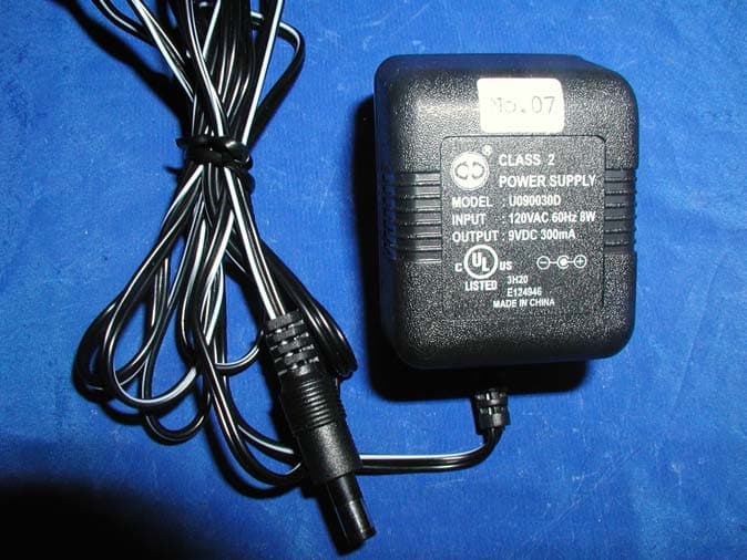
EUT Handset - Top View EUT Handset – Bottom View EUT Base – Top View EUT Base – Front View EUT Base – Rear View
ID Label/Location Info
FCC ID Label Specifications : Text is black or white in color and is left justified. Labels are silk-screened and shall be “permanently affixed” at a conspicuous location on the EUT. Proposed Label Location on EUT Rear Side of EUT Base/Proposed FCC ID Label Location / Top Side of Handset FCC Warning Statement According to FCC 15.19 (a) (3) and (5), all device shall bear the following statement in a conspicuous location on the device: “This device complies with Part 15 of The FCC Rules. Operation is subject to the following two conditions: (1) this device may not cause harmful interference, and (2) this device must accept any interference received, including interference that may cause undesired operation.” When the device is so small or for such use that it is not practicable to place the statement specified on it, the information required shall be placed in a prominent location in the instruction manual or pamphlet supplied to the user or, alternatively, shall be placed on the container in which the device is marketed. However, the FCC identifier or the unique identifier, as appropriate, must be displayed on the device. According to FCC 15.214 (c), the label shall also contain the following statement: “Privacy of communications may not be ensured when using this phone.”
Internal Photos
EUT Handset - Main Board Component View EUT Handset – Main Board Solder View EUT Handset – Transmitter View 1 EUT Handset – Transmitter View 2 EUT Base – Component View EUT Base – Main Board Solder View EUT Base – Transmitter View 1 EUT Base – Transmitter Solder View
Operational Description
LIONDA TECHNOLOGY COMPANY LIMITEDLIONDA TECHNOLOGY COMPANY LIMITED ENGINEERING DEPARTMENTENGINEERING DEPARTMENT IBM3850desc Page 1 10-Oct-01 CIRCUIT DESCRIPTION Model: IBM-3850 Base a. RF Transmitter Section – RF Board Compressed audio signal is frequency modulated through the varactor diode D3, D4. Diode D3, D4, L4 and Q5 the external components formed the voltage controlled oscillator circuit for the transmitter part. This circuit generates the TX VCO frequency. A portion of this signal is fed back to the PLL IC’s pin1 (FIN1) for phase comparison. Once the phase of oscillation stabilized, the PLL circuit generates the error voltage necessary for the VCO to oscillate at the desired transmitter’s RF frequency. The VCO circuit impedance is matched with the succeeding circuit through the transistor Q2 that also acts as the buffer amplifier. RF amplifier Q7 boosts the signal for transmission. This amplified RF signal is trimmed to the desired frequency band by BPF2403 so as not to interfere with the receiver circuit. The transmitter RF signal is then propagated through the antenna. b. RF Receiver Section - RF Board The Base Unit antenna receives RF signal. Band Pass Filter BPF2475 trims the signal to the desirable frequency band. Transistor Q6 & Q3 is a low noise amplifier that boosts the RF signal to a specific level for mixing. PLL IC1 (KB8825B) is used as a Universal Phase Lock Loop circuit. The frequency from the Voltage Controlled Oscillator (VCO) D1, L5 and Q4, is fed back to the PLL IC through pin 16 (FIN2) for phase comparison. During channel scanning or turning the unit on, once the phase of oscillation stabilized (locked), the PLL circuit generates the first local oscillator frequency for down-converting the received RF signal into the first IF frequency 10.7MHz. This process is accomplished through the IF mixer circuit Q1. Q1 is used for matching the impedance of the mixer circuit with the succeeding circuits. The resulting IF signal is kept constant by the IF Filter FL1 to 10.7MHz which is then mixed with the second local oscillator frequency 11.150MHz (derived from X1 & C47) to produced a much lower IF frequency. This lower IF frequency if further filtered by IF Filter FL4 to produce a more stable signal of 450AKHz. Quadrature signal detection is accomplished internally by the Narrow-band Detector IC2 (KA3361) with the IF coil L7. The recovered audio frequency can be taken from IC2 audio output pin9. Double conversion of received signal is utilized to improve the image frequency rejection of the unit. c. Transmitter Audio Section – Main Board Audio Frequency signal from the telephone line is compressed through the compressor part of IC4 to minimize the transmission noise. The degree of compression depends on the external RC combinations. AGC is also utilized by IC4 to avoid shock noise caused by abrupt change of audio levels. The compressed audio is filtered and amplified for better acoustical performance. d. Receiver Audio Section – Main Board The compressed Audio Frequency signal is passed through passive RC filters for acoustic compliance. The filtered audio is then fed to the Compander IC4 for expansion thus retrieving the original Audio signal with noise filtered out. Q5 is used as buffer circuit. Bridge rectifier D12-D15 isolates the high-voltage telephone line to the rest of the circuit. D12-D15 is 1 LIONDA TECHNOLOGY COMPANY LIMITEDLIONDA TECHNOLOGY COMPANY LIMITED ENGINEERING DEPARTMENTENGINEERING DEPARTMENT IBM3850desc Page 2 10-Oct-01 also act as a hybrid transformer to create a two-way path for audio transmission to and reception from the telephone line. Handset b. RF Transmitter Section – RF Board Refer to portion 1.b for this section. All circuit performance is the same except that Band Pass Filter BPF2403 is changed to BPF2475 for the handset transmission. b. RF Receiver Section – RF Board Refer to portion 1.b for this section. All circuit performance is the same except that Band Pass Filter BPF2475 is changed to BPF2403 for the handset reception. c. Transmitter Audio Section – Main Board Audio Frequency signal from the handset or from the headset microphone is compressed through the compressor part of IC1 to minimize the transmission noise. The degree of compression depends on the external RC combinations. AGC is also utilized by IC1 to avoid shock noise caused by abrupt change of audio levels. The compressed audio is filtered and amplified for better acoustical performance. Q3 is a switching transistor that controls the power supply for the TX RF part. d. Receiver Audio Section – Main Board The compressed Audio Frequency signal is passed through passive RC filters for acoustic compliance. The filtered audio is then fed to the Compander IC1 for expansion thus retrieving the original audio signal with noise filtered out. Q2 & Q10 act as audio amplifier to sufficiently drive the handset speaker. Q7 and Q8 are switching transistors that control the power supply for the RF part, the Compander part and the AF amplifier respectively. An earphone jack is provided for an optional headset unit for handsfree conversation on the handset. OTHERS (Handset): a. Charging and Reset Controls Recharging the handset battery is accomplished by putting the handset on the cradle. IC5 detects this action and sends a command to the CPU for proper exchange of security code. b. Ring Detection When the handset receives the ring command from the base unit, the CPU will send buzzer signal to the ringer amplifier Q5 and Q6 that drives the Buzzer. OTHERS (Base): a. Hook Switching and Dialing Hook switching and the transistor Q6 that is controlled by the CPU accomplishes pulse dialing. DTMF signal from the ladder circuit internal to the CPU is filtered and amplified by Q5. 3 4 2 LIONDA TECHNOLOGY COMPANY LIMITEDLIONDA TECHNOLOGY COMPANY LIMITED ENGINEERING DEPARTMENTENGINEERING DEPARTMENT IBM3850desc Page 3 10-Oct-01 b. Over-voltage Protection Fuse1 and varistor Z1 act as high current and high…
Text truncated - open the document above for the full version.
Schematics
3850bm.sch-1 - Tue Oct 09 08:57:44 2001 IBM3850hrf2.sch-1 - Tue Oct 09 08:56:01 2001 IBM3850hm.sch-1 - Tue Oct 09 08:59:40 2001 IBM3850brf2.sch-1 - Tue Oct 09 08:53:36 2001
Test Report
Note: This report is only good for this company and model, it may not be duplicated without prior written consent of Bay Area Compliance Laboratory Corporation. This report must not be used by the client to claim product endorsement by NVLAP or any agency of the U.S. Government. FCC PART 15 Subpart C EMI MEASUREMENT AND TEST REPORT For SHENZHEN BAOAN HANTONG ELECTRONICS FACTORY Block 11 & 12 Jinbi Industrial Area, Hwang Tian, Baoan, Shenzhen, China FCC ID: OK8IBM3850 November 6, 2001 This Report Concerns: Original Report Equipment Type: Cordless Telephone– Household Appliances Test Engineer: Jeff Lee Test Date: October 15, 2001 Reviewed By: John Y. Chan – Engineering Manager Prepared By: Bay Area Compliance Laboratory Corporation 230 Commercial Street, Suite 2 Sunnyvale, CA 94085 Tel (408) 732-9162 Fax (408) 732-9164 SHENZHEN BAOAN HANTONG ELECTRONICS FACTORY FCC ID: OK8IBM3850 Report # R0110052 Page 2 of 19 FCC Part 15 Subpart C Test Report TABLE OF CONTENTS 1 – GENERAL INFORMATION .................................................................................................................................3 1.1 PRODUCT DESCRIPTION FOR EQUIPMENT UNDER TEST (EUT) ..............................................................................3 1.2 OBJECTIVE.............................................................................................................................................................3 1.3 RELATED SUBMITTAL(S)/GRANT(S) ......................................................................................................................3 1.4 TEST METHODOLOGY............................................................................................................................................3 1.5 TEST FACILITY.......................................................................................................................................................3 1.6 TEST EQUIPMENT LIST...........................................................................................................................................4 1.7 LOCAL SUPPORT EQUIPMENT LIST AND DETAILS...................................................................................................4 1.8 EXTERNAL I/O CABLING LIST AND DETAILS.........................................................................................................4 2 – SYSTEM TEST CONFIGURATION ....................................................................................................................5 2.1 DESCRIPTION OF TEST CONFIGURATION................................................................................................................5 2.2 EQUIPMENT MODIFICATIONS.................................................................................................................................5 2.3 CONFIGURATION OF TEST SYSTEM.........................................................................................................................6 2.4 TEST SETUP BLOCK DIAGRAM...............................................................................................................................6 3 – TEST SUMMARY...................................................................................................................................................7 4 – CONDUCTED EMISSIONS TEST DATA ...........................................................................................................8 4.1 MEASUREMENT UNCERTAINTY..............................................................................................................................8 4.2 EUT SETUP............................................................................................................................................................8 4.3 SPECTRUM ANALYZER SETUP................................................................................................................................8 4.4 TEST PROCEDURE..................................................................................................................................................9 4.5 SUMMARY OF TEST RESULTS.................................................................................................................................9 4.6 CONDUCTED EMISSIONS TEST DATA.....................................................................................................................9 4.7 PLOT OF CONDUCTED EMISSIONS TEST DATA.......................................................................................................9 5 – RADIATED EMISSION DATA...........................................................................................................................11 5.1 MEASUREMENT UNCERTAINTY............................................................................................................................11 5.2 EUT SETUP..........................................................................................................................................................11 5.3 SPECTRUM ANALYZER SETUP..............................................................................................................................11 5.4 TEST PROCEDURE................................................................................................................................................12 5.5 CORRECTED AMPLITUDE & MARGIN CALCULATION...........................................................................................12 5.6 SUMMARY OF TEST RESULTS...............................................................................................................................12 5.7 RADIATED EMISSIONS TEST RESULT DATA.........................................................................................................13 6 – BAND EDGES TESTING.....................................................................................................................................15 6.1 TEST PROCEDURE........................…
Text truncated - open the document above for the full version.
Test Setup Photos
Base Conducted Emission Photograph – Front View Base Conducted Emission Photograph – Rear View Base Radiated Emission Photograph – Front View Base Radiated Emission Photograph – Rear View Handset Radiated Emission Photograph – Front View Handset Radiated Emission Photograph – Rear View
Contact Information
Applicant
Dan Coronia(Senior Engineer)
Test Firm
Bay Area Compliance LaboratoryJohn Chan
Technical Specifications
| # | Rule Parts | Frequency Range | Power Output |
|---|---|---|---|
| 2 | 15C | 2.47 GHz - 2.48 GHz | - |
Other Applications from Shenzhen Baoan Hantong Electronics Factory
OK8ATC2488HT03
Jun 16, 20032.4 GHz 77 Chs DSSS Telephone with Caller ID
Equipment Class
DSS - Part 15 Spread Spectrum Transmitter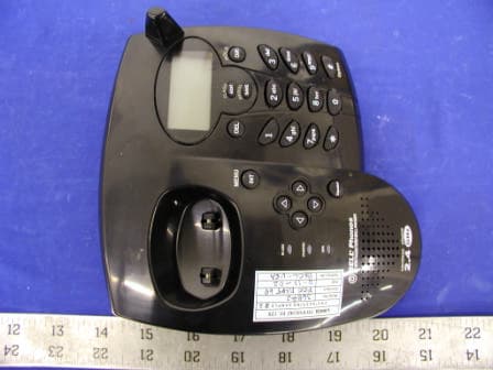
OK836882HT02
Feb 26, 20032.4 GHz Cordless Telephone
Equipment Class
DXX - Part 15 Low Power Communication Device Transmitter
OK839285HT02
Jan 21, 2003900 MHz Cordless Telephone
Equipment Class
DXX - Part 15 Low Power Communication Device Transmitter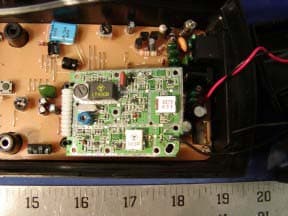
OK839287HT02
Dec 19, 2002900MHz Crdls Caller ID Phn w/ Call Waiting on H/S
Equipment Class
DXT - Part 15 Low Power Transceiver, Rx Verified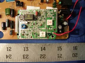
OK836280HT02
Dec 19, 20022.4GHz Filtered TM Snd 50-Chnnl Autoscan Crdls Phn
Equipment Class
DXT - Part 15 Low Power Transceiver, Rx Verified