OK8TT3860HT022.4GHz 50Chnnl Anlg Crdls Phn w/ Spkr & CID & CW
Shenzhen Baoan Hantong Electronics Factory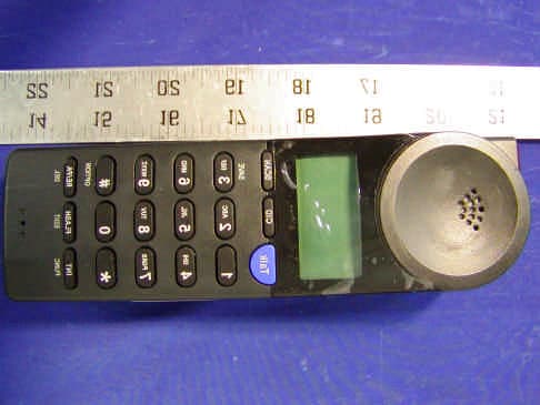
Click to zoom
Application Details
- Equipment Class
- DXT - Part 15 Low Power Transceiver, Rx Verified
- Date of Grant
- Aug 07, 2002
- Application Purpose
- Original Equipment
- Date of Application
- Aug 07, 2002
- Equipment Note
- 2.4GHz 50Chnnl Anlg Crdls Phn w/ Spkr & CID & CW
- Frequency Range
- 2472.21000000 - 2476.94000000
- Country
- China
Documents & Files
Document Text
Text extracted from the exhibit documents filed with the FCC. Open a document above to read the original.
Users Manual
MODEL: PMP-3860 2.4GHZ CORDLESS TELEPHONE WITH CALL WAITING CALLER ID AND SPEAKERPHONE IMPORTANT:To receive Caller ID information on incoming telephone calls, you must subscribe to the Caller ID service provided by your local telephone company; there is a fee for this service and it may not be available in all areas. 600-0921201-B INSTALLATION AND OPERATING GUIDE This symbol is to alert you to important operating or servicing instructions that may appear in the user's manual. Always follow basic safety precautions when using this product to reduce the risk of injury, fire, or electrical shock. When using this product, basic safety precautions should always be followed to reduce the risk of fire, electric shock and injury to persons, including the following: 1.Read and understand all instructions. 2.Follow all warnings and instructions marked on the product. 3.Use only with class 2 power source DC 9V 300mA. 4.Unplug this product from the wall outlet before cleaning. Do not use liquid cleaners or aerosol cleaners. Use a damp cloth for cleaning. 5.Do not use this product near water; for example, near a bathtub, wash bowl, kitchen sink or laundry tub, in a wet basement or near a swimming pool. 6.Do not place this product on an unstable cart, stand, or table. The product may fall, causing serious damage to the product. 7.Slots and openings in the cabinet back or bottom are provided for ventilation. To protect it from overheating, these openings must not be blocked or covered. The openings should never be blocked by placing the product on the bed, sofa, rug, or other similar surface. This product should never be placed near or over a radiator or heat register. This product should not be placed in an enclosed environment unless proper ventilation is provided. 8.Do not allow anything to rest on the power cord. Do not locate this product where the cord will be abused by animals or persons walking on it. 9.Do not overload wall outlets and extension cords as this can result in risk of fire or electrical shock. 10. Never push objects of any kind into this product through cabinet slots as they may touch dangerous voltage points or short out parts that could result in a risk of fire or electrical shock. Never spill liquid of any kind on the product. 11. To reduce the risk of electrical shock, do not disassemble this product. Instead take it to a qualified service person when service or repair work is required. Opening or removing covers may expose you to dangerous voltages or other risks. Incorrect re-assembly can cause electrical shock when the appliance is subsequently used. 12. Unplug all cords and refer servicing to qualified service personnel under the following conditions: A. When the power supply cord or plug is damaged or frayed. B. If liquid has been spilled into the product. C. If the product has been exposed to rain or water. D. If the product does not operate normally by following the operating instructions. Adjust only those controls covered in the operating instructions. Improper adjustment of other controls may result in damage and require work by a qualified technician to restore the product to normal operation. 13. Avoid using a telephone (other than a cordless type) during an electrical storm. There may be a remote risk of electric shock from lightning. 14. Do not use a telephone to report a gas leak in the vicinity of the leak. IF YOUR PRODUCT UTILIZES BATTERIES, THE FOLLOWING ADDITIONAL PRECAUTIONS SHOULD BE OBSERVED: 1.There is danger of the battery exploding if it is incorrectly installed. When inserting the batteries into this product, the proper polarity or direction must be observed. Reverse battery insertion can cause charging that may result in leakage or explosion. 2.Use only the type and size of batteries specified in the users manual. 3.Do not dispose of batteries in a fire. The cells may explode. Check with local codes for possible special disposal instructions. 4.Do not open or mutilate the batteries. Released electrolyte is corrosive and may cause damage to the eyes or skin. It may be toxic if swallowed. 5.Exercise care in handling batteries in order not to short the battery with conducting materials such as rings, bracelets and keys. The battery or conductor may overheat and cause burns. 6.Do not attempt to recharge the batteries with or identified for use with this product. The batteries may leak corrosive electrolyte or explode. 7.Do not attempt to rejuvenate the batteries provided with or identified for use with this product by heating them. Sudden release of the battery electrolyte may occur causing burns or irritation to eyes or skin. 8.When replacing batteries, all batteries should be replaced at the same time. Mixing fresh and discharged batteries could increase internal cell pressure and rupture the discharged batteries. 9.Remove the batteries from this product if the product will not be used for a long period of time (several months or more) since during this time the batteries could leak, damaging the product. 10. Discard "dead" batteries as soon as possible since they are more likely to leak in a product. 11. Do not store this product, or the batteries provided with or for identified use with this product, in high temperature areas. 12. If your product uses a rechargeable battery, charge the battery(ies) only in accordance with the instructions and limitation specified in the User Manual. SAVE THESE INSTRUCTIONS IMPORTANT SAFETY INSTRUCTIONS 2 Important Safety Instructions ...................2 FCC Regulations....................................3-4 Battery Cautionary Instructions ...............5 PMP-3860 Parts Checklist .........................6 Location of Controls and Features......7-12 Handset .................................................7-8 Base ...................................................9-11 LCD Display ...........................................12 Choosing a Location ...............................13 Telephone Setup.......................…
Text truncated - open the document above for the full version.
Block Diagram
3860HM.sch-1 - Tue Jul 16 10:57:59 2002 slc_npartgd_npartdescriprevQtyreference 128-2297-102ACAP_C_C.H.D. B0.001uF/K(0603) X:X7R282LP01C125 128-2297-103ACAP_C_C.H.D. B0.01uF/K(0603) X:X7R282LP04C33,C86,C91,C95 128-22A9-104ACAP_C_C.H.D. F0.1uF/Z(0603) Y:YF153LP016C3,C4,C5,C38,C40,C70,C102,C103,C104,C106,C107,C88 128-22A9-104ACAP_C_C.H.D. F0.1uF/Z(0603) Y:YF153LP00C114,C115,C116,C117 128-23A9-104ACAP_C_C.H.D. F0.1uF/Z(0805) Y:YF153LP01C2 128-23A9-105ACAP_C_C.H.D. F 1uF/Z(0805) Y:YF153LP01C60 128-2297-122ACAP_C_C.H.D. B0.0012uF/K(0603) X:X7R282LP01C25 128-2297-183ACAP_C_C.H.D. B0.018uF/K(0603) X:X7R282LP01C90 128-1216-200ACAP_C_CHIP 20PF/J(CH)(0603) A:COG150LP06C7,C34,C92,C109,C118,C124 128-1216-221ACAP_C_CHIP 220PF/J(CH)(0603) A:COG150LP02C10,C85 128-2297-223ACAP_C_C.H.D. B0.022uF/K(0603) X:X7R282LP03C55,C87,C89 128-1216-300ACAP_C_CHIP 30PF/J(CH)(0603) A:COG150LP02C96,C97 128-23A9-474ACAP_C_C.H.D.F0.47uF/Z(0805) Y:YF153LP03C35,C84,C120 12A-2032-101ACAP_E_MINI 100uF/16V(D6XL7)P01C83 12A-2022-221ACAP_E_MINI 220uF/10V( D6.3XL7)P02C82,C94 12B-1133-4R7ACAP_T_CHIP 4.7uF/M/10V(3.2X1.6)P02C80,C121 12B-1223-470ACAP_T_CHIP 47uF/M/6.3V(3.5X2.8)P02C98,C108 114-1207-001ADIODE_SW LL4148/MM4148 MELFP09D1,D4,D5,D6,D7,D9,D10,D11,D14 111-2103-002AIC_LI KA8507BD/8507D (SOP)P01U2 114-6108-001ADIODE_SW KDS184 (SOT-23)P02D2,D3 111-1204-012AIC_uP KS57P5616(QFP-100) O.T.P H/SP02U1 113-4400-002ALCD KXG32970AEP FOR 9934P01LCD1 113-1022-001ALED RED ELT-3348CP01LED1 113LEDP04LED2,LED3,LED4,LED5 122-0224-101ARES_(0603)-10 100 OHMP02R59,R76 122-0224-104ARES_(0603)-10 100 KOHMP05R10,R80,R93,R95,R118 122-0224-103ARES_(0603)-10 10 KOHMP013R4,R7,R11,R54,R55,R61,R75,R84,R92,R94,R107 122-0224-103ARES_(0603)-10 10 KOHMP00R117,R121 122-0224-123ARES_(0603)-10 12 KOHMP01R101 122-0224-154ARES_(0603)-10 150 KOHMP01R66 122-0224-153ARES_(0603)-10 15 KOHMP02R103,R62 122-0224-181ARES_(0603)-10 180 OHMP01R12 122-0224-184ARES_(0603)-10 180 KOHMP01R67 122-0224-102ARES_(0603)-10 1 KOHMP04R2,R68,R99,R120 122-0224-105ARES_(0603)-10 1 MOHMP01R35 122-0224-222ARES_(0603)-10 2.2 KOHMP03R21,R50,R85 122-0224-272ARES_(0603)-10 2.7 KOHMP01R108 122-0224-223ARES_(0603)-10 22 KOHMP05R23,R25,R30,R79,R109 122-0224-273ARES_(0603)-10 27 KOHMP01R70 122-0224-333ARES_(0603)-10 33 KOHMP02R57,R73 122-0224-472ARES_(0603)-10 4.7 KOHMP01R112 122-0224-470ARES_(0603)-10 47 OHMP01R58 122-0224-471ARES_(0603)-10 470 OHMP03R9,R19,R56 122-0224-473ARES_(0603)-10 47 KOHMP04R22,R69,R45,R106 122-0224-563ARES_(0603)-10 56 KOHMP02R1,R60 122-0224-682ARES_(0603)-10 6.8 KOHMP02R43,R102 122-0224-821ARES_(0603)-10 820 OHMP06R13,R14,R15,R16,R81,R83 122-0224-823ARES_(0603)-10 82 KOHMP01R74 111-3103-006BIC_COM R1121N331B SSOP-5P01U5 112-1106-001ATR_SS KST2907TF/KTN2907S/AS /MMBT2907LT1(SOT-23)P02Q12,Q14 112-1306-001CTR_SS MMBT3904LT1(SOT-23)P010Q1,Q2,Q3,Q4,Q8,Q9,Q10,Q11,Q13,Q19 123-3224-503ACHIP SVR 50 KOHMP02SVR1,SVR2 12C-1220-003AXTAL_4.19 MHz(20PF) HC-49S H:3.58mmP01X2 115-0207DIODE_ZEN. BZX55C5V1 (5.1V/0.5W)P01ZD1 122-0324-000ARES_(0805)-10 0 OHMP01J00 5A1-4074-061APCBA_RF HANDSET DOUBLE 2.4GHZ REV:01P01PCBA_RF 142-0155-A33AFLAT_CABLE 11P/15mm/2.0PITCH(3-3) (NON-UL)P01 340-0500-011BZEBRA PAPER 56X12.5X0.6(PITCH) HUAXINGP01 146-2121-002ASWITCH_FUNCTION IT-1207-3180P04OPTION,DIR,UP,DOWN 146-1522-001ASWITCH._VOL.(THREE SPEED)SK-13D01(VG2.0) 9003VP01SW1 134-5200-001AEARPHONE JACK(2.6mm) ST-020 SMT(STEREO) FOR 39230P01PH1 122-0224-562ARES_(0603)-10 5.6 KOHMA1R64 122-0224-000ARES_(0603)-10 0 OHMA1R71 122-0224-220ARES_(0603)-10 22 OHMA1R77 122-0224-512ARES_(0603)-10 5.1 KOHMA1R65 111-6103-001CIC_MEM. 24LC32A (MICROCHIP) SOP-8P01U1 smt Y Y Y Y Y Y Y Y Y Y Y Y Y Y Y Y Y Y Y Y Y Y Y Y Y Y Y Y Y Y Y Y Y Y Y Y Y Y Y Y Y Y Y Y Y Y Y Y Y Y Y Y Y Y Y Y slc_npart g descrip rev Qty reference smt 111-2107-001A IC_LI KA78L05AZ/LM78L05 (TO-92) P0 1 IC3 128-1216-101A CAP_C_CHIP 100PF/J(CH)(0603) A:COG150L P0 3 C14,C98,C123 Y 128-2297-102A CAP_C_C.H.D. B0.001uF/K(0603) X:X7R282L P0 2 C42,C68 Y 129-1254-102A CAP_M_GEN 0.001uF/K 250V(H12XF4) P0 4 C4,C12,C47,C48 128-2297-103A CAP_C_C.H.D. B0.01uF/K(0603) X:X7R282L P0 7 C15,C16,C58,C100,C101,C119,C129 Y 128-22A9-104A CAP_C_C.H.D. F0.1uF/Z(0603) Y:YF153L P0 37 C2,C5,C19,C21,C30,C32,C38,C45,C50,C52,C53,C55,C57,C63 Y 128-22A9-104A CAP_C_C.H.D. F0.1uF/Z(0603) Y:YF153L P0 0 C67,C72,C79,C80,C82,C88,C90,C97,C102,C106,C117,C120, Y 128-22A9-104A CAP_C_C.H.D. F0.1uF/Z(0603) Y:YF153L P0 0 C1,C8,C54,C33,C51,C54,C59,C124,C125,C126 Y 128-1213-100A CAP_C CHIP 10PF/D/(CH)/(0603) A:COG150L P0 1 C44 Y 128-2297-152A CAP_C_C.H.D. B0.0015uF/K(0603) X:X7R282L P0 1 C37 Y 128-23A9-105A CAP_C_C.H.D. F 1uF/Z(0805) Y:YF153L P0 3 C73,C74.C111 Y 128-1216-200A CAP_C_CHIP 20PF/J(CH)(0603) A:COG150L P0 1 C7 Y 129-1154-222A CAP_M_GEN 0.0022uF/250V/K(F12XF3.5) P0 1 C23 128-2297-223A CAP_C_C.H.D. B0.022uF/K(0603) X:X7R282L P0 2 C6,C110 Y 128-1216-220A CAP_C_CHIP 22PF/J(CH)(0603) A:COG150L P0 2 C20,C56 Y 128-1216-270A CAP_C_CHIP 27PF/J(CH)(0603) A:COG150L P0 2 C114,C115 Y 128-1216-331A CAP_C_CHIP 330PF/J(CH)(0603) A:COG150L P0 2 C17,C39 Y 128-1216-391A CAP_C_CHIP 390PF/J(CH)(0603) A:COG150L P0 1 C26 Y 128-22A8-473A CAP_C_C.H.D. F0.047uF/M(0603) Y:YF153L P0 3 C10,C11,C69 Y 128-23A9-474A CAP_C_C.H.D.F0.47uF/Z(0805) Y:YF153L P0 1 C65 Y 128-2297-562A CAP_C_C.H.D. B0.0056uF/K(0603) X:X7R282L P0 1 C36 Y 128-2297-682A CAP_C_C.H.D. B0.0068uF/K(0603) X:X7R282L P0 1 C122 Y 12C-1210-006A XTAL_3.579545MHz (16P) P0 1 X3 114-2305-002A DIODE_REC 1N4003 P0 1 D1 114-2305-001A DIODE_REC 1N4004 P0 4 D3,D8,D9,D10 114-1204-001A DIODE_SW 1N4148 P0 2 D13,D16 134-1000-001A D.C. JACK INSERT TYPE DG-210/TX3-2Z P0 1 J2 12A-2052-R47A CAP_E_MINI 0.47uF/50V(D4XL7) P0 2 C34,C121 12A-2022-101A CAP_E_MINI 100uF/10V(D5XL7) P0 4 C41,C61,C76,C84 12A-2042-100A CAP_E_MINI 10uF/25V(D4XL7) P0 5 C60,C64,C70,C81,C128 12A-2052-010A CAP_E_MINI 1uF/50V(D4XL7) P0 2 C35,C77 12A-2032-221A CAP_E_MINI 220uF/16V( D8XL9) P0 1 C116 12A-2422-471A CAP_E_MINI 470uF/10V(D8XL7) P0 1 C31 12A-1032-471A CAP_E_GEN 470uF/16V (D8XL12) P0 2 C13,C118 12A-…
Text truncated - open the document above for the full version.
Cover Letter(s)
SHENZHEN BAOAN HANTONG ELECTRONICS FACTORY Block 11 & 12, Jinbi Industrial Area, Hwangtian, Baoan, Shenzhen, China. TEL.: +86-755-7506252 FAX: +86-755-7506248 July 8, 2002 Federal Communications Commission 7435 Oakland Mills Road Columbia, Maryland, 21046 Sir/Madam, Reg: FCC grand for OK8TT3860HT02 This letter is an authorization to accept Bay Area Compliance Lab. Corporation as an agent for Shenzhen Baoan Hantong Electronics Factory located at Block 11 & 12 Jinbi Industrial Area, Hwang Tian, Baoan, Shenzhen, China , to sign applications before the Commission on our behalf, to make representations to you on our behalf, and to receive and exchange data between our company and the commission in connection with certification of the following Shenzhen Baoan Hantong Electronics Factory Product: 2.4GHz 50-Channel Analog Cordless Telephone with Caller ID and Call Waiting on Handset. and Speakerphone on the Base. Model Name: PMP-3860XX, PMG-3860XX, IBM-3860XX, BE-3860XX, TT-3860XX, SB-3860XX Under FCC docket number 20780 and general docket number 80-284 pursuant to part 15, FCC rules and regulations. Sincerely, Signature : Printed Name : Dan Coronia Title : Senior Engineer
External Photos
EXHIBIT C - EUT PHOTOGRAPHS Handset – Keypad Handset – Back Base – Keypad Base – Rear Base – Port
ID Label/Location Info
EXHIBIT A - FCC PRODUCT LABELING AND WARNING STATEMENT FCC ID Label Specifications: Text is black or white in color and is left justified. Labels are silk-screened and shall be “permanently affixed” at a conspicuous location on the EUT. Proposed Label Location on EUT Bottom Side of Base/Proposed FCC ID Label Location / Handset FCC Warning Statement A FCC Warning Statement is provided in the product manual. FCC ID: EW780-1005-00 This device complies with Part 15 of the FCC Rules. Operation is subject to the following two conditions: (1) this device may not cause harmful interference, and (2) this device must accept any interference received, including interference that may cause undesired operation. Privacy of communications may not be ensured when using this phone. 2.1875" 1.0" Label FCC ID: OK8TT3860HT02
Internal Photos
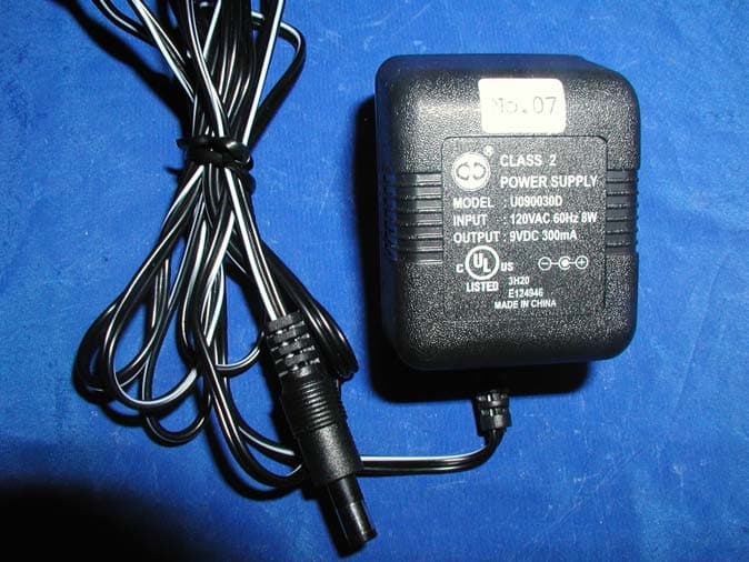
Handset – Component Handset – Solder Handset Transmitter – Component Handset Transmitter – Solder Base – Component Base – Solder Base Transmitter – Component Base Transmitter – Solder Handset – Battery Base – Power Adapter
Operational Description
LIONDA TECHNOLOGY COMPANY LIMITED Lionda Research and Development Center PMP3860 TestMode.doc 1 08/13/02 Test Mode Procedure for PMP-3860XX Note: The default channel frequency is CH25 for both the Base Unit (B/U) and the Handset (H/S). Refer to the Frequency Table for proper frequency allocations. Base Basic Test Mode: Insert the 12Vdc plug into the B/U DC jack while pressing the “Page” key. Both RX and TX will be activated and basic testing can be done. Press the “Page” key to scan the channel frequency one at a time. Handset: Insert the battery into the H/S battery socket while pressing the “*” key. Both RX and TX will be activated and basic testing can be done. Press the “*” key to scan the channel frequency one at a time. LIONDA TECHNOLOGY COMPANY LIMITED Lionda Research and Development Center PMP3860 TestMode.doc 2 08/13/02 2.4GHz PMP-3860XX FREQUENCY CHART B A S E H A N D S E T B A S E H A N D S E T CH TX RX TX RX CH TX RX TX RX 1 2400.592 2472.215 2472.215 2400.592 26 2403.002 2474.625 2474.625 2403.002 2 2400.688 2472.312 2472.312 2400.688 27 2403.098 2474.722 2474.722 2403.098 3 2400.785 2472.408 2472.408 2400.785 28 2403.195 2474.818 2474.818 2403.195 4 2400.881 2472.504 2472.504 2400.881 29 2403.291 2474.914 2474.914 2403.291 5 2400.977 2472.601 2472.601 2400.977 30 2403.387 2475.011 2475.011 2403.387 6 2401.074 2472.697 2472.697 2401.074 31 2403.484 2475.107 2475.107 2403.484 7 2401.170 2472.794 2472.794 2401.170 32 2403.580 2475.204 2475.204 2403.580 8 2401.267 2472.890 2472.890 2401.267 33 2403.677 2475.300 2475.300 2403.677 9 2401.363 2472.986 2472.986 2401.363 34 2403.773 2475.396 2475.396 2403.773 10 2401.459 2473.083 2473.083 2401.459 35 2403.869 2475.493 2475.493 2403.869 11 2401.556 2473.179 2473.179 2401.556 36 2403.966 2475.589 2475.589 2403.966 12 2401.652 2473.276 2473.276 2401.652 37 2404.062 2475.686 2475.686 2404.062 13 2401.749 2473.372 2473.372 2401.749 38 2404.159 2475.782 2475.782 2404.159 14 2401.845 2473.468 2473.468 2401.845 39 2404.255 2475.878 2475.878 2404.255 15 2401.941 2473.565 2473.565 2401.941 40 2404.351 2475.975 2475.975 2404.351 16 2402.038 2473.661 2473.661 2402.038 41 2404.448 2476.071 2476.071 2404.448 17 2402.134 2473.758 2473.758 2402.134 42 2404.544 2476.168 2476.168 2404.544 18 2402.231 2473.854 2473.854 2402.231 43 2404.640 2476.264 2476.264 2404.640 19 2402.327 2473.950 2473.950 2402.327 44 2404.737 2476.360 2476.360 2404.737 20 2402.423 2474.047 2474.047 2402.423 45 2404.833 2476.457 2476.457 2404.833 21 2402.520 2474.143 2474.143 2402.520 46 2404.930 2476.553 2476.553 2404.930 22 2402.616 2474.240 2474.240 2402.616 47 2405.026 2476.650 2476.650 2405.026 23 2402.713 2474.336 2474.336 2402.713 48 2405.122 2476.746 2476.746 2405.122 24 2402.809 2474.432 2474.432 2402.809 49 2405.219 2476.842 2476.842 2405.219 25 2402.905 2474.529 2474.529 2402.905 50 2405.315 2476.939 2476.939 2405.315
RF Exposure Info
LIONDA TECHNOLOGY COMPANY LIMITED ENGINEERING DEPARTMENT PMP3860desc.doc Page 1 8/13/2002 CIRCUIT DESCRIPTION Model: PMP-3860XX Base a. RF Transmitter Section – RF Board Compressed audio signal is frequency modulated through the varactor diode D3, D4. Diode D3, D4, L4 and Q5 the external components formed the voltage controlled oscillator circuit for the transmitter part. This circuit generates the TX VCO frequency. A portion of this signal is fed back to the PLL IC’s pin1 (FIN1) for phase comparison. Once the phase of oscillation stabilized, the PLL circuit generates the error voltage necessary for the VCO to oscillate at the desired transmitter’s RF frequency. The VCO circuit impedance is matched with the succeeding circuit through the transistor Q2 that also acts as the buffer amplifier. RF amplifier Q7 boosts the signal for transmission. This amplified RF signal is trimmed to the desired frequency band by BPF2403 so as not to interfere with the receiver circuit. The transmitter RF signal is then propagated through the antenna. b. RF Receiver Section - RF Board The Base Unit antenna receives RF signal. Band Pass Filter BPF2475 trims the signal to the desirable frequency band. Transistor Q6 & Q3 is a low noise amplifier that boosts the RF signal to a specific level for mixing. PLL IC1 (KB8825B) is used as a Universal Phase Lock Loop circuit. The frequency from the Voltage Controlled Oscillator (VCO) D1, L5 and Q4, is fed back to the PLL IC through pin 16 (FIN2) for phase comparison. During channel scanning or turning the unit on, once the phase of oscillation stabilized (locked), the PLL circuit generates the first local oscillator frequency for down-converting the received RF signal into the first IF frequency 10.7MHz. This process is accomplished through the IF mixer circuit Q1. Q1 is used for matching the impedance of the mixer circuit with the succeeding circuits. The resulting IF signal is kept constant by the IF Filter FL1 to 10.7MHz which is then mixed with the second local oscillator frequency 11.150MHz (derived from X1 & C47) to produced a much lower IF frequency. This lower IF frequency if further filtered by IF Filter FL4 to produce a more stable signal of 450AKHz. Quadrature signal detection is accomplished internally by the Narrow-band Detector IC2 (KA3361) with the IF coil L7. The recovered audio frequency can be taken from IC2 audio output pin9. Double conversion of received signal is utilized to improve the image frequency rejection of the unit. c. Transmitter Audio Section – Main Board 1 LIONDA TECHNOLOGY COMPANY LIMITED ENGINEERING DEPARTMENT PMP3860desc.doc Page 2 8/13/2002 Audio Frequency signal from the telephone line is compressed through the compressor part of IC4 to minimize the transmission noise. The degree of compression depends on the external RC combinations. AGC is also utilized by IC4 to avoid shock noise caused by abrupt change of audio levels. The compressed audio is filtered and amplified for better acoustical performance. d. Receiver Audio Section – Main Board The compressed Audio Frequency signal is passed through passive RC filters for acoustic compliance. The filtered audio is then fed to the Compander IC4 for expansion thus retrieving the original Audio signal with noise filtered out. Q5 is used as buffer circuit. Bridge rectifier D12-D15 isolates the high-voltage telephone line to the rest of the circuit. D12-D15 is also act as a hybrid transformer to create a two-way path for audio transmission to and reception from the telephone line. Handset b. RF Transmitter Section – RF Board Refer to portion 1.b for this section. All circuit performance is the same except that Band Pass Filter BPF2403 is changed to BPF2475 for the handset transmission. b. RF Receiver Section – RF Board Refer to portion 1.b for this section. All circuit performance is the same except that Band Pass Filter BPF2475 is changed to BPF2403 for the handset reception. c. Transmitter Audio Section – Main Board Audio Frequency signal from the handset or from the headset microphone is compressed through the compressor part of IC1 to minimize the transmission noise. The degree of compression depends on the external RC combinations. AGC is also utilized by IC1 to avoid shock noise caused by abrupt change of audio levels. The compressed audio is filtered and amplified for better acoustical performance. Q3 is a switching transistor that controls the power supply for the TX RF part. d. Receiver Audio Section – Main Board The compressed Audio Frequency signal is passed through passive RC filters for acoustic compliance. The filtered audio is then fed to the Compander IC1 for expansion thus retrieving the original audio signal with noise filtered out. Q2 & Q10 act as audio amplifier to sufficiently drive the handset speaker. Q7 and Q8 are 2 2 LIONDA TECHNOLOGY COMPANY LIMITED ENGINEERING DEPARTMENT PMP3860desc.doc Page 3 8/13/2002 switching transistors that control the power supply for the RF part, the Compander part and the AF amplifier respectively. An earphone jack is provided for an optional headset unit for handsfree conversation on the handset. OTHERS (Handset): a. Charging and Reset Controls Recharging the handset battery is accomplished by putting the handset on the cradle. IC5 detects this action and sends a command to the CPU for proper exchange of security code. b. Ring Detection When the handset receives the ring command from the base unit, the CPU will send buzzer signal to the ringer amplifier Q5 and Q6 that drives the Buzzer. OTHERS (Base): a. Hook Switching and Dialing Hook switching and the transistor Q6 that is controlled by the CPU accomplishes pulse dialing. DTMF signal from the ladder circuit internal to the CPU is filtered and amplified by Q5. b. Over-voltage Protection Fuse1 and varistor Z1 act as high current and high voltage protectors for the telephone line interface. In case of presence of voltage surge across the telephone line, Fuse1 decreases its resistance and …
Text truncated - open the document above for the full version.
Schematics
3860HM.sch-1 - Tue Jul 16 10:57:59 2002 slc_npartgd_npartdescriprevQtyreference 128-2297-102ACAP_C_C.H.D. B0.001uF/K(0603) X:X7R282LP01C125 128-2297-103ACAP_C_C.H.D. B0.01uF/K(0603) X:X7R282LP04C33,C86,C91,C95 128-22A9-104ACAP_C_C.H.D. F0.1uF/Z(0603) Y:YF153LP016C3,C4,C5,C38,C40,C70,C102,C103,C104,C106,C107,C88 128-22A9-104ACAP_C_C.H.D. F0.1uF/Z(0603) Y:YF153LP00C114,C115,C116,C117 128-23A9-104ACAP_C_C.H.D. F0.1uF/Z(0805) Y:YF153LP01C2 128-23A9-105ACAP_C_C.H.D. F 1uF/Z(0805) Y:YF153LP01C60 128-2297-122ACAP_C_C.H.D. B0.0012uF/K(0603) X:X7R282LP01C25 128-2297-183ACAP_C_C.H.D. B0.018uF/K(0603) X:X7R282LP01C90 128-1216-200ACAP_C_CHIP 20PF/J(CH)(0603) A:COG150LP06C7,C34,C92,C109,C118,C124 128-1216-221ACAP_C_CHIP 220PF/J(CH)(0603) A:COG150LP02C10,C85 128-2297-223ACAP_C_C.H.D. B0.022uF/K(0603) X:X7R282LP03C55,C87,C89 128-1216-300ACAP_C_CHIP 30PF/J(CH)(0603) A:COG150LP02C96,C97 128-23A9-474ACAP_C_C.H.D.F0.47uF/Z(0805) Y:YF153LP03C35,C84,C120 12A-2032-101ACAP_E_MINI 100uF/16V(D6XL7)P01C83 12A-2022-221ACAP_E_MINI 220uF/10V( D6.3XL7)P02C82,C94 12B-1133-4R7ACAP_T_CHIP 4.7uF/M/10V(3.2X1.6)P02C80,C121 12B-1223-470ACAP_T_CHIP 47uF/M/6.3V(3.5X2.8)P02C98,C108 114-1207-001ADIODE_SW LL4148/MM4148 MELFP09D1,D4,D5,D6,D7,D9,D10,D11,D14 111-2103-002AIC_LI KA8507BD/8507D (SOP)P01U2 114-6108-001ADIODE_SW KDS184 (SOT-23)P02D2,D3 111-1204-012AIC_uP KS57P5616(QFP-100) O.T.P H/SP02U1 113-4400-002ALCD KXG32970AEP FOR 9934P01LCD1 113-1022-001ALED RED ELT-3348CP01LED1 113LEDP04LED2,LED3,LED4,LED5 122-0224-101ARES_(0603)-10 100 OHMP02R59,R76 122-0224-104ARES_(0603)-10 100 KOHMP05R10,R80,R93,R95,R118 122-0224-103ARES_(0603)-10 10 KOHMP013R4,R7,R11,R54,R55,R61,R75,R84,R92,R94,R107 122-0224-103ARES_(0603)-10 10 KOHMP00R117,R121 122-0224-123ARES_(0603)-10 12 KOHMP01R101 122-0224-154ARES_(0603)-10 150 KOHMP01R66 122-0224-153ARES_(0603)-10 15 KOHMP02R103,R62 122-0224-181ARES_(0603)-10 180 OHMP01R12 122-0224-184ARES_(0603)-10 180 KOHMP01R67 122-0224-102ARES_(0603)-10 1 KOHMP04R2,R68,R99,R120 122-0224-105ARES_(0603)-10 1 MOHMP01R35 122-0224-222ARES_(0603)-10 2.2 KOHMP03R21,R50,R85 122-0224-272ARES_(0603)-10 2.7 KOHMP01R108 122-0224-223ARES_(0603)-10 22 KOHMP05R23,R25,R30,R79,R109 122-0224-273ARES_(0603)-10 27 KOHMP01R70 122-0224-333ARES_(0603)-10 33 KOHMP02R57,R73 122-0224-472ARES_(0603)-10 4.7 KOHMP01R112 122-0224-470ARES_(0603)-10 47 OHMP01R58 122-0224-471ARES_(0603)-10 470 OHMP03R9,R19,R56 122-0224-473ARES_(0603)-10 47 KOHMP04R22,R69,R45,R106 122-0224-563ARES_(0603)-10 56 KOHMP02R1,R60 122-0224-682ARES_(0603)-10 6.8 KOHMP02R43,R102 122-0224-821ARES_(0603)-10 820 OHMP06R13,R14,R15,R16,R81,R83 122-0224-823ARES_(0603)-10 82 KOHMP01R74 111-3103-006BIC_COM R1121N331B SSOP-5P01U5 112-1106-001ATR_SS KST2907TF/KTN2907S/AS /MMBT2907LT1(SOT-23)P02Q12,Q14 112-1306-001CTR_SS MMBT3904LT1(SOT-23)P010Q1,Q2,Q3,Q4,Q8,Q9,Q10,Q11,Q13,Q19 123-3224-503ACHIP SVR 50 KOHMP02SVR1,SVR2 12C-1220-003AXTAL_4.19 MHz(20PF) HC-49S H:3.58mmP01X2 115-0207DIODE_ZEN. BZX55C5V1 (5.1V/0.5W)P01ZD1 122-0324-000ARES_(0805)-10 0 OHMP01J00 5A1-4074-061APCBA_RF HANDSET DOUBLE 2.4GHZ REV:01P01PCBA_RF 142-0155-A33AFLAT_CABLE 11P/15mm/2.0PITCH(3-3) (NON-UL)P01 340-0500-011BZEBRA PAPER 56X12.5X0.6(PITCH) HUAXINGP01 146-2121-002ASWITCH_FUNCTION IT-1207-3180P04OPTION,DIR,UP,DOWN 146-1522-001ASWITCH._VOL.(THREE SPEED)SK-13D01(VG2.0) 9003VP01SW1 134-5200-001AEARPHONE JACK(2.6mm) ST-020 SMT(STEREO) FOR 39230P01PH1 122-0224-562ARES_(0603)-10 5.6 KOHMA1R64 122-0224-000ARES_(0603)-10 0 OHMA1R71 122-0224-220ARES_(0603)-10 22 OHMA1R77 122-0224-512ARES_(0603)-10 5.1 KOHMA1R65 111-6103-001CIC_MEM. 24LC32A (MICROCHIP) SOP-8P01U1 smt Y Y Y Y Y Y Y Y Y Y Y Y Y Y Y Y Y Y Y Y Y Y Y Y Y Y Y Y Y Y Y Y Y Y Y Y Y Y Y Y Y Y Y Y Y Y Y Y Y Y Y Y Y Y Y Y slc_npart g descrip rev Qty reference smt 111-2107-001A IC_LI KA78L05AZ/LM78L05 (TO-92) P0 1 IC3 128-1216-101A CAP_C_CHIP 100PF/J(CH)(0603) A:COG150L P0 3 C14,C98,C123 Y 128-2297-102A CAP_C_C.H.D. B0.001uF/K(0603) X:X7R282L P0 2 C42,C68 Y 129-1254-102A CAP_M_GEN 0.001uF/K 250V(H12XF4) P0 4 C4,C12,C47,C48 128-2297-103A CAP_C_C.H.D. B0.01uF/K(0603) X:X7R282L P0 7 C15,C16,C58,C100,C101,C119,C129 Y 128-22A9-104A CAP_C_C.H.D. F0.1uF/Z(0603) Y:YF153L P0 37 C2,C5,C19,C21,C30,C32,C38,C45,C50,C52,C53,C55,C57,C63 Y 128-22A9-104A CAP_C_C.H.D. F0.1uF/Z(0603) Y:YF153L P0 0 C67,C72,C79,C80,C82,C88,C90,C97,C102,C106,C117,C120, Y 128-22A9-104A CAP_C_C.H.D. F0.1uF/Z(0603) Y:YF153L P0 0 C1,C8,C54,C33,C51,C54,C59,C124,C125,C126 Y 128-1213-100A CAP_C CHIP 10PF/D/(CH)/(0603) A:COG150L P0 1 C44 Y 128-2297-152A CAP_C_C.H.D. B0.0015uF/K(0603) X:X7R282L P0 1 C37 Y 128-23A9-105A CAP_C_C.H.D. F 1uF/Z(0805) Y:YF153L P0 3 C73,C74.C111 Y 128-1216-200A CAP_C_CHIP 20PF/J(CH)(0603) A:COG150L P0 1 C7 Y 129-1154-222A CAP_M_GEN 0.0022uF/250V/K(F12XF3.5) P0 1 C23 128-2297-223A CAP_C_C.H.D. B0.022uF/K(0603) X:X7R282L P0 2 C6,C110 Y 128-1216-220A CAP_C_CHIP 22PF/J(CH)(0603) A:COG150L P0 2 C20,C56 Y 128-1216-270A CAP_C_CHIP 27PF/J(CH)(0603) A:COG150L P0 2 C114,C115 Y 128-1216-331A CAP_C_CHIP 330PF/J(CH)(0603) A:COG150L P0 2 C17,C39 Y 128-1216-391A CAP_C_CHIP 390PF/J(CH)(0603) A:COG150L P0 1 C26 Y 128-22A8-473A CAP_C_C.H.D. F0.047uF/M(0603) Y:YF153L P0 3 C10,C11,C69 Y 128-23A9-474A CAP_C_C.H.D.F0.47uF/Z(0805) Y:YF153L P0 1 C65 Y 128-2297-562A CAP_C_C.H.D. B0.0056uF/K(0603) X:X7R282L P0 1 C36 Y 128-2297-682A CAP_C_C.H.D. B0.0068uF/K(0603) X:X7R282L P0 1 C122 Y 12C-1210-006A XTAL_3.579545MHz (16P) P0 1 X3 114-2305-002A DIODE_REC 1N4003 P0 1 D1 114-2305-001A DIODE_REC 1N4004 P0 4 D3,D8,D9,D10 114-1204-001A DIODE_SW 1N4148 P0 2 D13,D16 134-1000-001A D.C. JACK INSERT TYPE DG-210/TX3-2Z P0 1 J2 12A-2052-R47A CAP_E_MINI 0.47uF/50V(D4XL7) P0 2 C34,C121 12A-2022-101A CAP_E_MINI 100uF/10V(D5XL7) P0 4 C41,C61,C76,C84 12A-2042-100A CAP_E_MINI 10uF/25V(D4XL7) P0 5 C60,C64,C70,C81,C128 12A-2052-010A CAP_E_MINI 1uF/50V(D4XL7) P0 2 C35,C77 12A-2032-221A CAP_E_MINI 220uF/16V( D8XL9) P0 1 C116 12A-2422-471A CAP_E_MINI 470uF/10V(D8XL7) P0 1 C31 12A-1032-471A CAP_E_GEN 470uF/16V (D8XL12) P0 2 C13,C118 12A-…
Text truncated - open the document above for the full version.
Test Report
Note: This test report is specially limited to the above client company and the product model only. It may not be duplicated without prior written consent of Bay Area Compliance Laboratory Corporation. This report must not be used by the client to claim product endorsement by NVLAP or any agency of the U.S. Government. FCC PART 15 Subpart C EMI MEASUREMENT AND TEST REPORT For Shenzhen Baoan Hantong Electronics Factory Block 11 & 12, Jinbi Industrial Area Hwangtian, Baoan, Shenzhen, China FCC ID: OK8TT3860HT02 August 7, 2002 This Report Concerns: Original Report Equipment Type: 2.4GHz Cordless Telephone Test Engineer: Jeff Lee Report No.: R0206271 Test Date: July 15, 2002 Reviewed By: Jerry Wang Prepared By: Bay Area Compliance Laboratory Corporation 230 Commercial Street Sunnyvale, …
Text truncated - open the document above for the full version.
Contact Information
Applicant
Dan Coronia(Senior Engineer)
Test Firm
Bay Area Compliance LaboratoryJohn Chan
Technical Specifications
| # | Rule Parts | Frequency Range | Power Output |
|---|---|---|---|
| 2 | 15C | 2.47 GHz - 2.48 GHz | - |
Other Applications from Shenzhen Baoan Hantong Electronics Factory
OK8ATC2488HT03
Jun 16, 20032.4 GHz 77 Chs DSSS Telephone with Caller ID
Equipment Class
DSS - Part 15 Spread Spectrum Transmitter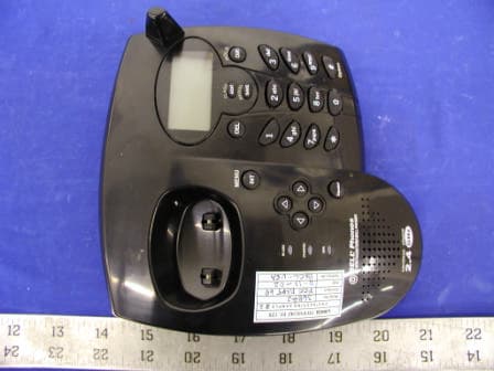
OK836882HT02
Feb 26, 20032.4 GHz Cordless Telephone
Equipment Class
DXX - Part 15 Low Power Communication Device Transmitter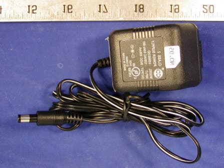
OK839285HT02
Jan 21, 2003900 MHz Cordless Telephone
Equipment Class
DXX - Part 15 Low Power Communication Device Transmitter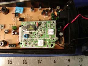
OK839287HT02
Dec 19, 2002900MHz Crdls Caller ID Phn w/ Call Waiting on H/S
Equipment Class
DXT - Part 15 Low Power Transceiver, Rx Verified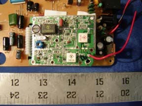
OK836280HT02
Dec 19, 20022.4GHz Filtered TM Snd 50-Chnnl Autoscan Crdls Phn
Equipment Class
DXT - Part 15 Low Power Transceiver, Rx Verified