ON3MRRE
Prastel S.p.A.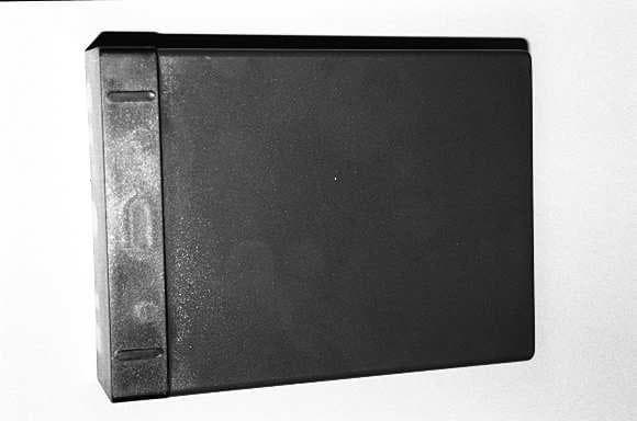
Click to zoom
Application Details
- Equipment Class
- CYY - Communications Receiver used w/Pt 15 Transmitter
- Date of Grant
- Dec 22, 1999
- Application Purpose
- Original Equipment
- Date of Application
- Nov 07, 1999
- Frequency Range
- 433.92000000 - 433.92000000
- Company
- Prastel S.p.A.
- Country
- Italy
Documents & Files
Document Text
Text extracted from the exhibit documents filed with the FCC. Open a document above to read the original.
Users Manual
MRRE ENGLISH MRRE_V0 Member of:Associated CAUTION FOR THE USER Any change or modification of the product is forbidden if not expressly approved by the manufacturer 0. DESCRIPTION The MRRE receiver was designed to be connected to access control central units as a radio reader. The code received from the transmitter is re-sent to the output terminals according to the format and protocol selected by means of the programming dip-switches. The formats available at the output are those most commonly used in access control systems. 1. TECHNICAL FEATURES Reception frequency433.92 MHz Output code formatWiegand, Dataclock, TTL, RS232 CodeDigital Power supply12 – 24 V ac/dc Average consumption30 mA Signalling devicesred LED 2. SELECTION OF OUTPUT FORMAT AND PROTOCOL WIEGAND DATA CLOCK TTL RS232 30 bit PRASTEL37 bit HID 26 bit INDALA26 bit without site code Standard ISO track 2: start sentinel + 16 digits + end sentinel Standard ISO track 2: start sentinel + 16 digits + separator +end sentinel + LRC 9600 baud, 8 bit, no parity, 1 stop MRRE ENGLISH MRRE_V0 Member of:Associated CHANNEL ADDRESS The MRRE receiver can be operated by one or more pushbuttons of the transmitters by means of the channel address dip-switches (see figure) OUTPUT LEVEL SELECTION A jumper on the circuit (see figure) makes it possible to select the level of the output signals in the Wiegand, Dataclock and TTL formats. CONNECTIONS 24 24 V ac/dc power supply GND Ground 12 12 V ac/dc power supply D0 Data output: Wiegand: DATA0 Data Clock: DATA TTL: DATA RS232: not used D1 Data output: Wiegand: DATA1 Data Clock: CLOCK TTL: NOT USED RS232: not used GND Ground EN Enable contact - Antenna shield ANT Antenna The EN terminal must be connected to GROUND to enable the receiver. Vout = 12 VVout = 5 V + - + 24 GND 12 D1 D0 GND EN ANT MRRE ENGLISH MRRE_V0 Member of:Associated FCC ID: ON3MRRE This device complies with part 15 of the FCC Rules. Operation is subject to the following two conditions: (1) this device may not cause harmful interference, and (2) this device must accept any interference received, including interference that may cause undesired operation. This equipment has been tested and found to comply with the limits for a Class B digital device, pursuant to Part 15 of the FCC Rules. These limits are designed to provide reasonable protection against harmful interference in a residential installation. This equipment generates, uses and can radiate radio frequency energy and, if not installed and used in accordance with the instructions, may cause harmful interference to radio communications. However, there is no guarantee that interference will not occur in a particular installation. If this equipment does cause harmful interference to radio or television reception, which can be determined by turning the equipment off and on, the user is encouraged to try to correct the interference by one or more of the following measures: -Reorient or relocate the receiving antenna. -Increase the separation between the equipment and receiver. -Connect the equipment into an outlet on a circuit different from that to which the receiver is connected. -Consult the dealer or an experienced radio/TV technician for help. RS232 output connector Channel address Output format and protocol selection Output level selection
Block Diagram
FCC ID : ON3MRRE Block diagram Pag. 1 BLOCK DIAGRAM(S) OF THE EUT Block Diagram Description The Controller Board of the EUT is provided with: - ceramic resonator X1 = 4 MHz Contained in PL118 radio module: - SAW resonator SAW2 = 423.22 MHz - Ceramic filter 10.7 MHz FCC ID : ON3MRRE Block diagram Pag. 2 Fig. 1 - Block Diagram of the EUT IN THE FOLLOWING PAGES YOU CAN FIND ALL THE INFORMATION ABOUT THE RADIO MODULE (PL118) WHICH IS INSERTED IN THE RECEIVER FCC ID : ON3MRRE Block diagram Pag. 3 PL118 electrical scheme FCC ID : ON3MRRE Block diagram Pag. 4 PL118 circuit layout FCC ID : ON3MRRE Block diagram Pag. 5 PL118 part list |----------------------------------------------------------------------------------------------------------------------------------------------------------| |Bill Of Materials for L9024F1.sch on Mon Mar 22 11:53:29 1999 | |----------------------------------------------------------------------------------------------------------------------------------------------------------| |Item|Qty |Ref. |Prastel Code |Name |Value |Tol. |Description | |----+-----+-----------------------------+----------------+--------------------+------------+------+-------------------------------------------------------| |1 |1 |A2 | |Manifacturing | | |Manufacturing | |2 |1 |A1 | |NOTE | | |Row Pitch, Dimension See Sample | |3 |1 |C24 |C10PCS |CSMD |10pF |NP0 |Ceramic Capacitor 0805 SMT | |4 |1 |C17 |C12PCS |CSMD |12pF |NP0 |Ceramic Capacitor 0805 SMT | |5 |5 |C3-4 C6-8 |C1N0CS |CSMD |1nF |Z5U |Ceramic Capacitor 0805 SMT | |6 |1 |C14 |C1P5CS |CSMD |1p5F |Z5U |Ceramic Capacitor 0805 SMT | |7 |3 |C9 C13 C26 |C2M2V10S |CSMD |2M2F10V | |Tantalum Capacitor CaseA SMT | |8 |1 |C11 |C2P2CS |CSMD |2p2F |NP0 |Ceramic Capacitor 0805 SMT | |9 |1 |C16 |C2P7CS |CSMD |2p7F |NP0 |Ceramic Capacitor 0805 SMT | |10 |1 |C15 |C33PCS |CSMD |33pF |NP0 |Ceramic Capacitor 0805 SMT | |11 |1 |C23 |C5P6CS |CSMD |5p6F |NP0 |Ceramic Capacitor 0805 SMT | |12 |2 |C1-2 |C8P2CS |CSMD |8p2F |NP0 |Ceramic Capacitor 0805 SMT | |13 |9 |C5 C10 C12 C18-22 C27 |CM10CS |CSMD |100nF |Z5U |Ceramic Capacitor 0805 SMT | |14 |1 |C25 |CN22CS |CSMD |220pF |X7R |Ceramic Capacitor 0805 SMT | |15 |1 |Z1 |CSL422-2 |L422-2 |0.8mm/35um | |PCB Double Side 18 x 48.5 mm | |16 |1 |D1 |D4148S |LL4148 | | |Signal Diode SOD80 SMT | |17 |3 |L1 L3 L5 |I15NHST5 |LSMD |15nH |5% |Inductor SIMID02 SMT | |18 |1 |L4 |I5UH6ST5 |LSMD |5M6H |5% |Inductor SIMID02 SMT | |19 |1 |U2 |ICLM358S |LM358 | | |Dual Op Amp 8pin SMT | |20 |1 |U1 |ICNE615D |NE615D | | |Low Power FM IF System SMT | |21 |1 |R12 |R10KS |RSMD |10K |5% |Resistor 0805 SMT | |22 |2 |R1-2 |R1K5S |RSMD |1K5 |5% |Resistor 0805 SMT | |23 |1 |R7 |R22KS |RSMD |22K |5% |Resistor 0805 SMT | |24 |1 |R6 |R27KS |RSMD |27K |5% |Resistor 0805 SMT | |25 |1 |R8 |R2K2S |RSMD |2K2 |5% |Resistor 0805 SMT | |26 |3 |R4 R10 R13 |R56KS |RSMD |56K |5% |Resistor 0805 SMT | |27 |1 |R5 |R56RS |RSMD |56 |5% |Resistor 0805 SMT | |28 |1 |R3 |R82KS |RSMD |82K |5% |Resistor 0805 SMT | |29 |1 |X1 |RISCER8 |SFECA10.7MA5-A | | |Ceramic Filter 10.7 MHz | |30 |1 |SAW2 |RISSAW4 |R2531 | | |SAW Resonator 423.22 MHz | |31 |2 |R9 R11 |RM10S |RSMD |100K |5% |Resistor 0805 SMT | |32 |1 |SC1 |SCPL118 | | | |Shield | |33 |1 |J1 |STRIPPIN(15P) |518-0718-0-42-111 | | |Soldering Terminals SIL 15P Center 2.54mm | |34 |3 |Q1-3 |TBFS17 |BFS17 | | |NPN Small Signal Transistor SOT23 SMT | |----------------------------------------------------------------------------------------------------------------------------------------------------------| FCC ID : ON3MRRE Block diagram Pag. 6 PL118 block diagram
External Photos
FCC ID : ON3MRRE External Photos Pag. 1 Fig. 1 Front view FCC ID : ON3MRRE External Photos Pag. 2 Fig. 2 Rear view
ID Label/Location Info
FCC ID : ON3MRRE ID label / Location info Pag. 1 PRODUCT LABELING Figure 1 FCC ID Label FCC ID: ON3MRRE This device complies with part 15 of the FCC Rules. Operation is subject to the following two conditions: (1) This device may not cause harmful interference, and (2) this device must accept any interference received, including interference that may cause undesired operation FCC ID : ON3MRRE ID label / Location info Pag. 2 Figure 2 Location of the Label on EUT
Internal Photos
FCC ID : ON3MRRE Internal Photos Pag. 1 Fig. 1 Controller Board - Components side FCC ID : ON3MRRE Internal Photos Pag. 2 Fig. 2 Controller Board - Foil side
Operational Description
FCC ID : ON3MRRE Operational description Pag. 1 GENERAL INFORMATION Product Description EUT is a receiver designed to be connected to access control central unit as a radio reader; it works on 433.920 MHz frequency. The code received from the transmitter is re-sent to the output terminals according to the format and protocol selected by means of the programming dip-switches. The formats available at the output are those most commonly used in access control systems. It is provided with an antenna connector to be used with the wire antenna provided or with an external antenna.
Parts List/Tune Up Info
FCC ID : ON3MRRE Part List Pag. 1 MRRE – part list |----------------------------------------------------------------------------------------------------------------------------------------------------------| |Bill Of Materials for L9033A1.sch on Tue Sep 07 14:00:38 1999 | |----------------------------------------------------------------------------------------------------------------------------------------------------------| |Item|Qty |Ref. |Prastel Code |Name |Value |Tol. |Description | |----+-----+-----------------------------+----------------+--------------------+------------+------+-------------------------------------------------------| |1 |1 |J3 | |Soldering Terminals | | | | | | | | |10p | | | | |2 |1 |JP1 | |JP4F OPT | | |Female Strip 4P 2.54 | |3 |1 |A1 | |Manifacturing | | |Manufacturing | |4 |4 |C9-10 C12 C14 |C10NC |CCE |10nF |Z5U |Ceramic Capacitor | |5 |6 |C1-5 C8 |C1MV35 |CEV |1MF35V | |Vertical Electrolytic Capacitor | |6 |2 |C11 C13 |C220V35 |CEV |220MF35V | |Vertical Electrolytic Capacitor | |7 |3 |C6-7 C15 |CM10C |CCE |100nF |Z5U |Ceramic Capacitor | |8 |1 |J1 |CONDB9F90 |DB9F90 | | |Female D Type Connector 9P 90 | |9 |1 |Z1 |CSL382-1 |L382-1 |1.6mm/35um | |PCB Double Side 95 X 100 mm | |10 |3 |D2-4 |D4007 |1N4007 | | |Rectifier Diode | |11 |1 |D1 |D4148 |1N4148 | | |Signal Diode | |12 |1 |DZ1 |D5V1W2 |DZ |5V1 | |Zener 1/2W | |13 |3 |SW1-3 |DIP4 |DIP-SW4 | | |4 Contacts Vertical D.I.L. Switch | |14 |1 |LD1 |DLED3R |LED03R | | |LED Diameter 3mm Red | |15 |2 |F1-2 |FUSA25R |R3-RXE-025 | | |MultiFuse 250mA | |16 |1 |L1 |IA02 |IA02 | | |Air Inductor for Antenna | |17 |1 |U1 |IC232 |MAX232 | | |Drivers/Receiver RS-232 | |18 |1 |U5 |IC78L05 |LM78L05 | | |Voltage Regulator | |19 |1 |U4 |IC78L12 |LM78L12 | | |Voltage Regulator | |20 |1 |U6 |IC93C66 |NMC93C66N | | |256-Bit Serial EEPROM | |21 |1 |U3 |ICPL114 |PL114 | | |433MHz Receiver SIL Hybrid Circuit with Filter | |22 |1 |U2 |ICPL773AP1 |PL773A | | |4 BIT Microcontroller | |23 |1 |J2 |MS09B |MKDS3/9-5.08 | | |Terminal 9P | |24 |3 |R9 R11 R15 |R10KW4 |RES |10K |5% |Resistor Carbon 1/4W | |25 |2 |R4-5 |R1K0W4 |RES |1K |5% |Resistor Carbon 1/4W | |26 |1 |R14 |R47KW4 |RES |47K |5% |Resistor Carbon 1/4W | |27 |1 |RR1 |R47KW4R8 |RR |47K |5% |Resistor Array 8+1 | |28 |2 |R6 R10 |R47RW4 |RES |47 |5% |Resistor Carbon 1/4W | |29 |1 |R16 |R4K7W4 |RES |4K7 |5% |Resistor Carbon 1/4W | |30 |1 |R12 |R56R1W |RES |56 1W |5% |Resistor Carbon 1W | |31 |3 |R1-3 |R5K6W4 |RES |5K6 |5% |Resistor Carbon 1/4W | |32 |1 |X1 |RISCER4 |CST4MGW |4MHz | |Ceramic Resonator | |33 |2 |R7-8 |RK56W4 |RES |560 |5% |Resistor Carbon 1/4W | |34 |1 |R13 |RM10W4 |RES |100K |5% |Resistor Carbon 1/4W | |35 |1 |JP2 |STRIPTP3P |JP3M | | |Male Strip 3P 2.54 | |36 |3 |Q1-3 |TBC237 |BC237B | | |NPN Small Signal Transistor | |37 |5 |TP1-5 |TPOINT |TP | | |Test-Point | |----------------------------------------------------------------------------------------------------------------------------------------------------------|
Schematics
FCC ID : ON3MRRE Schematics Pag. 1 MRRE – electrical scheme FCC ID : ON3MRRE Schematics Pag. 2 MRRE – circuit layout FCC ID : ON3MRRE Schematics Pag. 3 FCC ID : ON3MRRE Schematics Pag. 4 FCC ID : ON3MRRE Schematics Pag. 5 MRRE – block diagram
Test Report
Test Report No. RD99/167 FCC ID: ON3MRRE Date November 2nd, 1999 TÜV QSL 1/24 MEASUREMENT/TECHNICAL REPORT PRASTEL FCC ID: ON3MRRE November 2nd, 1999 This report concerns (check one): Original grant __X__ Class II change____ Equipment type: RECEIVER (ex.: computer, printer, modem, etc.) Deferred grant request per 47 CFR 0.457(d)(1)(ii)? yes _____ no __X__ If yes, defer until: ______________ date Company Name agrees to notify the Commission by ______________ date of the intended date of announcement of the product so that the grant can be issued on that date. Report prepared by: P.Antonio VELO Giuseppe MECCHIA TÜV QSL srl Via Montalenghe 12 10010 Scarmagno ( TO ) Italy Phone : 0125 - 525441 Phone : 0125 – 525440 Fax : 0125 – 525499 Test Report No. RD99/167 FCC ID: ON3MRRE Date November 2nd, 1999 TÜV QSL 2/24 Table of Contents Page 1GENERAL INFORMATION ........................................................ 3 1.1 Product Description ........................................................ 3 1.2 Related Submittal(s)/Grant(s).......................................... 3 1.3 Tested System Details..................................................... 4 1.4 Test Methodology ............................................................ 5 1.5 Test Facility..................................................................... 5 1.6 Test Equipment List......................................................... 5 2PRODUCT LABELING................................................................ 6 Figure 2.1 FCC ID Label ....................................................... 6 Figure 2.2 Location of the Label on EUT............................... 7 3SYSTEM TEST CONFIGURATION ............................................ 8 3.1 Justification...................................................................... 8 3.2 EUT Exercise Software.................................................... 8 3.3 Special Accessories ........................................................ 9 3.4 Equipment Modifications ................................................. 9 3.5 Configuration of the Tested System ................................ 10 Figure 3.1 Configuration of the Tested System...................... 10 4BLOCK DIAGRAM(S) OF THE EUT.. ......................................... 11 4.1 Block Diagram Description ............................................... 11 Figure 4.1 Block Diagram of the EUT.................................... 12 5CONDUCTED AND RADIATED MEASUREMENT PHOTOS..... 13 6CONDUCTED EMISSION DATA ................................................ 14 7RADIATED EMISSION DATA ..................................................... 15 7.2 Field Strength Calculation ............................................... 16 8PHOTOS OF TESTED EUT ....................................................... 17-23 User Manual (Draft Edition) ...............................................................24-Attached Test Report No. RD99/167 FCC ID: ON3MRRE Date November 2nd, 1999 TÜV QSL 3/24 1 GENERAL INFORMATION 1.1 Product Description EUT is a receiver designed to be connected to access control central unit as a radio reader; it works on 433.920 MHz frequency. The code received from the transmitter is re-sent to the output terminals according to the format and protocol selected by means of the programming dip-switches. The formats available at the output are those most commonly used in access control systems. It is provided with an antenna connector to be used with the wire antenna provided or with an external antenna. 1.2 Related Submittal(s)/Grant(s) None Test Report No. RD99/167 FCC ID: ON3MRRE Date November 2nd, 1999 TÜV QSL 4/24 1.3 Tested System Details The FCC IDs for all equipment, plus descriptions of all cables used in the tested system (including inserted cards, which have grants) are: Model & Serial No. FCC IDDescriptionCable Descriptions ----------------------------------------------------------------------------------------------------------- MRRE (1) s/n EMC-99-0277 ON3MRREReceiver Unshielded power cord Unshielded signal cable Comelit 542024T s/n 408390 noneAC adapterUnshielded power cord ANT/433SDnoneExternal antennaCoax cable M/2000 E s/n none noneAccess control unitUnshielded power cord Unshielded signal cable GVC GREEN753 s/n GND967190060 DK4GREEN753NotebookUnshielded power cord Unshielded signal cable ILAN F1560-P s/n 9602 noneAC adapter for notebook Unshielded power cords DM 119 s/n 3031602 DYKDM119Printer, parallel I/FUnshielded power cord Shielded signal cable (1) EUT submitted for grant. Test Report No. RD99/167 FCC ID: ON3MRRE Date November 2nd, 1999 TÜV QSL 5/24 1.4 Test Methodology Both conducted and radiated testing were performed according to the ANSI C63.4-1992 test procedures . Radiated testing was performed at an antenna to EUT distance of 3 meters. 1.5 Test Facility TÜV QSL test site No. 3 (semi-anechoic chamber) The semi-anechoic chamber test site and conducted measurement facility used to collect the radiated data are located at Via Montalenghe 12, Scarmagno, Italy. This site has been fully described in a report dated March 25, 1997 submitted to your office, and accepted in a letter dated August 4, 1997 (31040/SIT-1300F2). 1.6 Test equipment list: Test receiverRohde & Schwarz ESH3s/n 881364/012 LISNSchwarzbeck NNLA8120s/n 8120399 Test receiver/spectrum anal.HP 8568B+QP adapters/n 2601A02134 Biconical antennaTensor 4104s/n 2222 Log-periodic antenna Electro-metrix LPA-25s/n 1117 Spectrum analyzerHP 8562As/n 3043A05627 Horn antennaEMCO 3115s/n 3572 Test Report No. RD99/167 FCC ID: ON3MRRE Date November 2nd, 1999 TÜV QSL 6/24 2 PRODUCT LABELING Figure 2.1 FCC ID Label FCC ID: ON3MRRE This device complies with part 15 of the FCC Rules. Operation is subject to the following two conditions: (1) This device may not cause harmful interference, and (2) this device must accept any interference received, including interference that may cause undesired operation Test Report No. RD99/167 FCC ID: ON3MRRE Date No…
Text truncated - open the document above for the full version.
Test Report
Test Report No. RD99/167 FCC ID: ON3MRRE Date November 2nd, 1999 TÜV QSL 1/24 MEASUREMENT/TECHNICAL REPORT PRASTEL FCC ID: ON3MRRE November 2nd, 1999 This report concerns (check one): Original grant __X__ Class II change____ Equipment type: RECEIVER (ex.: computer, printer, modem, etc.) Deferred grant request per 47 CFR 0.457(d)(1)(ii)? yes _____ no __X__ If yes, defer until: ______________ date Company Name agrees to notify the Commission by ______________ date of the intended date of announcement of the product so that the grant can be issued on that date. Report prepared by: P.Antonio VELO Giuseppe MECCHIA TÜV QSL srl Via Montalenghe 12 10010 Scarmagno ( TO ) Italy Phone : 0125 - 525441 Phone : 0125 – 525440 Fax : 0125 – 525499 Test Report No. RD99/167 FCC ID: ON3MRRE Date November 2nd, 1999 TÜV QSL 2/24 Table of Contents Page 1GENERAL INFORMATION ........................................................ 3 1.1 Product Description ........................................................ 3 1.2 Related Submittal(s)/Grant(s).......................................... 3 1.3 Tested System Details..................................................... 4 1.4 Test Methodology ............................................................ 5 1.5 Test Facility..................................................................... 5 1.6 Test Equipment List......................................................... 5 2PRODUCT LABELING................................................................ 6 Figure 2.1 FCC ID Label ....................................................... 6 Figure 2.2 Location of the Label on EUT............................... 7 3SYSTEM TEST CONFIGURATION ............................................ 8 3.1 Justification...................................................................... 8 3.2 EUT Exercise Software.................................................... 8 3.3 Special Accessories ........................................................ 9 3.4 Equipment Modifications ................................................. 9 3.5 Configuration of the Tested System ................................ 10 Figure 3.1 Configuration of the Tested System...................... 10 4BLOCK DIAGRAM(S) OF THE EUT.. ......................................... 11 4.1 Block Diagram Description ............................................... 11 Figure 4.1 Block Diagram of the EUT.................................... 12 5CONDUCTED AND RADIATED MEASUREMENT PHOTOS..... 13 6CONDUCTED EMISSION DATA ................................................ 14 7RADIATED EMISSION DATA ..................................................... 15 7.2 Field Strength Calculation ............................................... 16 8PHOTOS OF TESTED EUT ....................................................... 17-23 User Manual (Draft Edition) ...............................................................24-Attached Test Report No. RD99/167 FCC ID: ON3MRRE Date November 2nd, 1999 TÜV QSL 3/24 1 GENERAL INFORMATION 1.1 Product Description EUT is a receiver designed to be connected to access control central unit as a radio reader; it works on 433.920 MHz frequency. The code received from the transmitter is re-sent to the output terminals according to the format and protocol selected by means of the programming dip-switches. The formats available at the output are those most commonly used in access control systems. It is provided with an antenna connector to be used with the wire antenna provided or with an external antenna. 1.2 Related Submittal(s)/Grant(s) None Test Report No. RD99/167 FCC ID: ON3MRRE Date November 2nd, 1999 TÜV QSL 4/24 1.3 Tested System Details The FCC IDs for all equipment, plus descriptions of all cables used in the tested system (including inserted cards, which have grants) are: Model & Serial No. FCC IDDescriptionCable Descriptions ----------------------------------------------------------------------------------------------------------- MRRE (1) s/n EMC-99-0277 ON3MRREReceiver Unshielded power cord Unshielded signal cable Comelit 542024T s/n 408390 noneAC adapterUnshielded power cord ANT/433SDnoneExternal antennaCoax cable M/2000 E s/n none noneAccess control unitUnshielded power cord Unshielded signal cable GVC GREEN753 s/n GND967190060 DK4GREEN753NotebookUnshielded power cord Unshielded signal cable ILAN F1560-P s/n 9602 noneAC adapter for notebook Unshielded power cords DM 119 s/n 3031602 DYKDM119Printer, parallel I/FUnshielded power cord Shielded signal cable (1) EUT submitted for grant. Test Report No. RD99/167 FCC ID: ON3MRRE Date November 2nd, 1999 TÜV QSL 5/24 1.4 Test Methodology Both conducted and radiated testing were performed according to the ANSI C63.4-1992 test procedures . Radiated testing was performed at an antenna to EUT distance of 3 meters. 1.5 Test Facility TÜV QSL test site No. 3 (semi-anechoic chamber) The semi-anechoic chamber test site and conducted measurement facility used to collect the radiated data are located at Via Montalenghe 12, Scarmagno, Italy. This site has been fully described in a report dated March 25, 1997 submitted to your office, and accepted in a letter dated August 4, 1997 (31040/SIT-1300F2). 1.6 Test equipment list: Test receiverRohde & Schwarz ESH3s/n 881364/012 LISNSchwarzbeck NNLA8120s/n 8120399 Test receiver/spectrum anal.HP 8568B+QP adapters/n 2601A02134 Biconical antennaTensor 4104s/n 2222 Log-periodic antenna Electro-metrix LPA-25s/n 1117 Spectrum analyzerHP 8562As/n 3043A05627 Horn antennaEMCO 3115s/n 3572 Test Report No. RD99/167 FCC ID: ON3MRRE Date November 2nd, 1999 TÜV QSL 6/24 2 PRODUCT LABELING Figure 2.1 FCC ID Label FCC ID: ON3MRRE This device complies with part 15 of the FCC Rules. Operation is subject to the following two conditions: (1) This device may not cause harmful interference, and (2) this device must accept any interference received, including interference that may cause undesired operation Test Report No. RD99/167 FCC ID: ON3MRRE Date No…
Text truncated - open the document above for the full version.
Test Setup Photos
FCC ID : ON3MRRE Test Setup Photos Pag. 1 Test Setup Photos CONDUCTED MEASUREMENT PHOTOS FCC ID : ON3MRRE Test Setup Photos Pag. 2 RADIATED MEASUREMENT PHOTOS
Contact Information
Applicant
Alberto Gamberini(R&D Engineer)
Test Firm
TUV ItaliaGiuseppe Mecchia
Technical Specifications
| # | Rule Parts | Frequency Range | Power Output |
|---|---|---|---|
| 1 | 15B | 433.92 MHz - 433.92 MHz | - |
Other Applications from Prastel S.p.A.
ON3TP2E
Apr 15, 2008GARAGE DOOR REMOTE CONTROL
Equipment Class
DSC - Part 15 Security/Remote Control Transmitter
ON3TXPR02
Apr 15, 2008GARAGE DOOR REMOTE CONTROL
Equipment Class
DSC - Part 15 Security/Remote Control Transmitter
ON3MPSDT2
Feb 02, 2000Proximity Sensor TX
Equipment Class
DXX - Part 15 Low Power Communication Device Transmitter
ON3MRAE
Jan 04, 2000LOW POWER RADIO RECEIVER
Equipment Class
CYY - Communications Receiver used w/Pt 15 Transmitter
ON3MPSTP2EB
Dec 21, 1999Garage Door Remote Control
Equipment Class
DSR - Part 15 Remote Control/Security Device Transceiver