OX6VDD21501Digitizer Monitor
ViewMate Electronic Technology LimitedApplication Details
- Equipment Class
- JBC - Part 15 Class B Computing Device/Personal Computer
- Date of Grant
- Aug 13, 2012
- Application Purpose
- Original Equipment
- Date of Application
- Aug 13, 2012
- Equipment Note
- Digitizer Monitor
- Country
- China
Documents & Files
Document Text
Text extracted from the exhibit documents filed with the FCC. Open a document above to read the original.
Users Manual
User’s Guide 21.5” LCD Tablet Monitor Series II | Safety Information Safety Information Read all of these instructions Save these instructions for later use, please. 1. Follow all warnings and instructions marked on the monitor. 2. This monitor should be operated only from the type of power source indicated on the marking label. If you are not sure of the type of power supplied in your home, consult your monitor dealer or local power company. 3. This monitor is equipped with a three-wire grounding type plug, a plug having a third (grounding) pin. This plug will only fit into grounding-type power outlet. This is a safety feature. If you are unable to insert the plug into the outlet, contact your electrician to replace your obsolete outlet. Do not defeat the safety purpose of the grounding-type plug. 4. The socket outlet shall be near the equipment and shall be easily accessible. Do not overload wall outlets and extension cords as this can result into fire or electric shock. 5. Do not allow anything to rest on the power cord. Do not locate this monitor where the cord will be abused by persons working on it. 6. Do not place this monitor on an unstable cart, stand, or table. The monitor may fall, causing serious injury to a child or adult and serious damage to the appliance. Use only with a cart or stand recommended by the manufacturer or sold with monitor. Wall or shelf mounting should follow the manufacturer’s instructions, and should use a mounting kit approved by the manufacturer. 7. Slots and openings in the cabinet and the back or bottom are provided for ventilation, and to insure reliable operation of the television receiver and to protect it from overheating, these openings must not be blocked or covered. The openings should never be blocked by placing the monitor on a bed, sofa, rug, or other similar surface. This monitor should never be placed near or over a radiator or heat register. This monitor should not be placed in built-in installation such as a bookcase unless proper ventilation is provided. Safety Information | III 8. Do not use this monitor near water. For example near a bathtub, washbowl, kitchen sink, or laundry tub, in a wet basement, or near a swimming pool, etc. 9. Unplug this monitor from the wall outlet before cleaning. Do not use liquid cleaners or aerosol cleaners. Use a damp cloth for cleaning. 10. Never push objects of any kind into this monitor through cabinet slots as they may touch dangerous voltage points or short out parts that could result in a fire or electric shock. Never spill liquid of any kind on the monitor. 11. For added protection for this monitor, when it is left unattended and unused for long periods of time, unplug it from the wall outlet. This will prevent damage to the monitor due to power-line surges. 12. Do not attempt to service this monitor yourself since opening or removing covers may expose you to dangerous voltage or other hazards. Refer all servicing to qualified service personnel. IV | Contents Contents 1. Introduction and Installing........................................................ 1 1.1 Packing List ..................................................................................1 1.2 Product Overview .........................................................................1 1.3 Tablet Driver Installing .................................................................4 1.4 Software Installation .....................................................................4 2. Setup and Operation Guide....................................................... 5 2.1 Recommend Display Resolution...................................................5 2.2 Screen Calibrating and Pen setup..................................................5 2.3 OSD Function and Setup...............................................................7 3.Troubleshooting ...................................................................... 9 3.1 Display problems ..........................................................................9 3.2 Interactive Pen Problems ............................................................10 4.Product Specifications .......................................................... 11 4.1 Monitor ....................................................................................... 11 4.2 Tablet...........................................................................................12 4.3 VGA Connector...........................................................................12 5.Appendix............................................................................... 13 Appendix A. Replacing the Pen tip ...................................................13 Appendix B. Factory set display modes............................................14 Introduction and Installing | 1 1. Introduction and Installing 1.1 Packing List After unpacking, make sure that all of the following contents are included: z Tablet Monitor z Power adapter and power cord z Pen Kits Package z VGA and USB 2 in 1 cable (attached) z User’s guide and Driver CD If there is a defect or missing part, please contact the agency where you purchased the product. 1.2 Product Overview 1.2.1 Front View ① Display and pen touch area 。 ① ② ③ 2 | Introduction and Installing ② Power indication: When the monitor is working, the indicator turns steady green. When the monitor is in saving mode, the indicator turns flickering. ③ Control buttons: :Power on/off :Menu and Enter :Move Adjustment (up) :Move Adjustment (down) :VGA output switch 1.2.2 Side View ④ Stand: allow you to adjust it to an optimal viewing angle. CAUTION: Make sure the angle of the monitor is at least 10 degrees from the vertical; otherwise the monitor will be unstable and could fall over. 1.2.3 Rear View ⑤ VGA input cable: Plug it into VGA port of your computer. ④ ⑤ ⑥ ⑧ ⑨ ⑦ Introduction and Installing | 3 ⑥ USB cable: Plug it into USB port of your computer. ⑦ DC input: Plug the adapter port to DC input socket. ⑧ VGA output: to …
Text truncated - open the document above for the full version.
Block Diagram
21.5inch Digitizer Monitor Working principle Control board Digitizer TFT Panel Touch PEN Input PC USB Touch Pen 12V Power suppler 12V Power suppler VGA Input HDMI Input VGA Output Oscillator 14.318Mhz
External Photos
VDD21501
ID Label/Location Info
FCC ID: OX6VDD21501 Label Location on EUT ID Label: FCC ID: OX6VDD21501 This device complies with Part 15 of the FCC Rules. Operation is subject to the following two conditions: (1) this device may not cause harmful interference, and (2) this device must accept any interference received, including interference that may cause undesired operation. MADE IN CHINA
Internal Photos
VDD21501
Operational Description
Circuit description: 1:Power supply: AC adapter : Output 12V 4A 2:Video signal:1: The control board accept the video signal form PC by HDMI or VGA, 2: The control board converts the HDMI or VGA signal to LVDS signal and delivers it to panel, 3: The panel accept the LVDS signal and display it on the panel. The control board can output VGA signal for other Monitor. 3:Touch signal:1: The touch pen send the wireless signal to digitizer TFT panel, 2: Digitizer TFT panel Identify the wireless signal and send the coordinate signal to the PC. 3:The PC will accept the coordinate signal and analyze it 4:The controller is TSUMU58EDJ, The frequency of oscillator is 14.318M
Schematics
Thursday, July 07, 2011 C 1 S1 TOP TSUMU58EDJ 7 of Sheet Date: Rev Document Number SizeTitle TSUMU58EDJ SCHEMATIC LVDS OUTPUT APPROVE BY PREPARE BY CHECK BY ABCD 5 4 3 2 1 DCBA 1 2 3 4 5 VSIN_IN BIN1GIN1RIN1RGBHV_CONTROL HSI HSIN_IN VSI A7 VCC3_3VCC1_8 HSYNCGINSOGVSYNCGNDGBINGNDRRINGNDBDDCA_SDADDCA_SCLDDCD_SDADDCD_SCLR-B+R+B-CLK+CLK-G+G-VCTRLDET_VGAON_PANEL +5V HPD_CTRLON_BACKLIGHTADJ_BACKLIGHT VCC5V CEC_CTRL RGBHV_CONTROL A4 BL_ON BL_ADJ 12V+5V A6 RIN GIN BIN VSYNC GNDR GNDG GNDB DET_VGA HSYNC SOG DDCA_SDA DDCA_SCL B- G+ G- R- CLK- R+ CLK+ B+ DDCD_SDA DDCD_SCL VGA5V HPD_CTRL VCC5VCEC_CTRLVCC3_3HDMI5VVSIHSIHSIN_INVSIN_IN BIN1 RIN1 GIN1 A3 VLCD A5 ON_PANEL VLCD VCTRL VCC1_8VCC3_3VGA5V+5V ON_BACKLIGHT ADJ_BACKLIGHT VCC5VHDMI5V BL_ON BL_ADJ 12V A2 VCC3_3 VGA5V +5V VLCD VGA5V VCC1_8 +5V VLCD VCC5V VCC5V VCC3_3 VCC1_8 VCC5V HDMI5V CEC_CTRL CEC_CTRL VCC3_3 HDMI5V 12V12V +5V VSI VSI HSI HSI HSIN_IN HSIN_IN VSIN_IN VSIN_IN BIN1 BIN1 RIN1 RIN1 GIN1 GIN1 PB[0:9]PA[0:9] C 7 -1 S1 common board POWER of Sheet Date: Rev Document Number SizeTitle Q2 for 19", Q2+Q10 for 22" CHECK BY PREPARE BY APPROVE BY 琍琍 , る 14 ら ,2005 ABCD 5 4 3 2 1 DCBA 1 2 3 4 5 4 4 3,4,6 4 5 4 4 3,4 3,4 3 3,4,6 3,4 3 6 6 6 3 1 2 Q1 NC/CHT2907 C110.1uF 3 1 2 Q6 MMBT3904 R11 10K/NC 3 1 2 D3 BAV70-GS08 3 VIN 1 ADJ 2 VOUT U2LT1084/TO263-33 C7NC/0.1u R9 4K7 C120.1uF 3 1 2 Q2 CHT2907 R1 10K R5 10K 1 VIN 2 PGND 3 AGND 4 FB 8 LX 7 LX 6 EN 5 COMP U1AOZ1013 C4 1000PF C6NC/0.1u D1 SR34 R3 10K + TC2 100uF + TC1 100uF L2 6.8uH R13 4K7 3 1 2 Q3 MMBT3904L + C910uF/16V TC3 47uF/25V D2 1N4001 G DS Q5AO3401 C80.1uF C100.1uF R6 4K7 1 2 L1 L1812 MLB-201209-0220P-N2 R1010K R12 100 C3 0.1uf 3 1 2 Q4 MMBT3904L 543 2 1 J1DCJACK D4 SSM12L R8 10K R230K RC210K R4 10K R710K C2 10UF C1 0.1uf RC1 52.3K C5 NC/1uF F1 24V/5A ADJ_BACKLIGHT ON_BACKLIGHT +5V ON_PANEL VLCD VCTRL VCC1_8 VCC3_3 VCC3_3 HDMI5V +5V VCC5V VGA5V 12V BL_ADJ BL_ON +5V +5V +5V +5V +5V VLCD VCC3_3 VCC1_8 +5V VCC3_3 +5V +5V VCC5V 12V VGA5V BL_ADJ BL_ON Tuesday, July 05, 2011 C -1 7 PANEL INTERFACE TSUMU58EDJ S1 of Sheet Date: Rev Document Number SizeTitle APPROVE BY PREPARE BY CHECK BY ABCD 5 4 3 2 1 DCBA 1 2 3 4 5 2 1 2 3 4 5 6 7 8 9 10 11 12 13 14 15 16 17 18 19 20 21 22 23 24 25 26 JP1 HEADER 13X2 VLCD VLCD PA[0:9]PB[0:9] RXO3- RXO3- LVBCKM LVBCKM RXO0- RXO0- RXE0- RXE0- RXO2- RXO2- RXE1+ RXE1+ RXEC- RXEC- RXE0+ RXE0+ RXO0+ RXO0+ RXO3+ RXO3+ RXE2- RXE2- RXE3+ RXE3+ RXE1- RXE1- RXE3- RXE3- LVBCKP LVBCKP RXO1+ RXO1+ RXO2+ RXO2+ RXO1- RXO1- RXE2+ RXE2+ RXEC+ RXEC+ RXO3- RXO3-LVBCKM LVBCKM RXO0- RXO0- RXE0- RXE0-RXO2- RXO2- RXE1+ RXE1+ RXEC- RXEC- RXE0+ RXE0+ RXO0+ RXO0+ RXO3+ RXO3+ RXE2- RXE2- RXE3+ RXE3+ RXE1- RXE1- RXE3- RXE3- LVBCKP LVBCKP RXO1+ RXO1+ RXO2+ RXO2+ RXO1- RXO1- RXE2+ RXE2+ RXEC+ RXEC+ Tuesday, July 12, 2011 C S1 TSUMU58EDJ INPUT 7 -1 of Sheet Date: Rev Document Number SizeTitle APPROVE BY PREPARE BY CHECK BY Chang I2CR29,R30,R31,R32,R33,R34,R35,R36 from10k to 2k,from100 to 33. 2008.09.09firmware zhang 2011.06.28 2011.06.28 CN1A 在 PCB 上上上上 CN1 包包包 CN1A(IN VGA) 和 P11 ( B 型 USB ) ABCD 5 4 3 2 1 DCBA 1 2 3 4 5 44 4 4 44 4 4 4 4 44 4 4 44 4 4 4 4 44 4 2,4 2 2,4 4 2 4 4 4 5 5 R46 10 C18 0.047uF D10MLL5232B 5.6V C19 0.047uF R48 10 3 1 2 D6BAV99 R47 10 C310.1uF R14 56 1/16W 5 VDD 6 #4 3 #2 4 #3 2 GND 1 #1 D18 AZ1045-04SU C33NC/0.1uF C20 0.1uF R44 NC R17 470 1/16W C280.1uF D8 MLL5232B 5.6V R21 100 1/16W C30NC C2433p R43 10 R37 1K 1/16W R42 10 D14 LL5232B 5.6V 5% C250.1uF R32 33 /100 1/16W 3 1 2 D5BAV99 R29 444444444444444 D15LL5232B 5.6V 5% R272.2K 1/16W R35 33 1/16W /100 R20 75 1/16W R39 NC/27K C26NC C29NC R23 100 1/16W 1 A0 2 A1 3 A2 4 GND 5 SDA 6 SCL 7 WP 8 VCC U3AT24C02N-10SC C21 0.1uF R16 56 1/16W R22 100 1/16W R15 56 1/16W R30 444444444444444 R38 4K7 C17 0.047uF C14 0.047uF D16NC/LL5232B 5.6V 5% 162738495 1112131415 10 17 16 CN1A DB15 R33444 5 VDD 6 #4 3 #2 4 #3 2 GND 1 #1 D17 AZ1045-04SU C13 0.047uF FB1 120 OHM BEAD C22 0.1uF C16 1000pF R34444 3 1 2 D7BAV99 D12MLL5232B 5.6V R25 1K 1/16W 3 1 2 Q7MMBT3904 C2333pF 1 A0 2 A1 3 A2 4 GND 5 SDA 6 SCL 7 WP 8 VCC U4AT24C02N-10SC D11 MLL5232B 5.6V C15 0.047uF D9MLL5232B 5.6V R40 10 R31 33 /100 1/16W C32NC/0.1uF R282.2K 1/16W R36 33 1/16W /100 1 3 2 Q8 NC/2N7002 R19 75 1/16W R45 10 1 1 2 2 3 3 4 4 5 5 6 6 7 7 8 8 9 9 10 10 11 11 12 12 13 13 14 14 15 15 16 16 17 17 18 18 19 19 20 20 CN1 HEADER444X2 3 DAT2- 1 DAT2+ 5 DAT1_SHIELD 15 DDC_SCL 16 DDC_SDA 6 DAT1- 4 DAT1+ 2 DAT2_SHIELD 18 +5V 17 CEC/DDC_GND 19 HPD 9 DAT0- 7 DAT0+ 8 DAT0_SHIELD 11 CLK_SHIELD 10 CLK+ 12 CLK- 13 CEC 20 20 21 21 22 22 23 23 CON1 DVI CON R18 75 1/16W R41 10 D13 LL5232B 5.6V 5% C27NC R26 1K 1/16W 1234 CON39CON4_2.0 R2410K 1/16W R58 3444 RINGINBINVSYNCGNDRGNDGGNDBDET_VGAHSYNCSOG DDCA_SDADDCA_SCL B-G+G-R-CLK-R+CLK+B+ DDCD_SDADDCD_SCL HPD_CTRL VCC5V VGA5V VCC3_3 CEC_CTRL HDMI5V HSIVSI RIN1 BIN1 GIN1 HSIN_INVSIN_IN VGA5V +5V HDMI5V +5V VCC5V VCC5V VCC3_3 +5V +5V +5V +5V_USB1 VGA5V DET_VGA DGND DAT0+ USB1_D1-_IN DAT_DDC HPD USB1_D1+_IN DAT2+DCLK+DAT2-DAT1+DCLK-DAT0- HDMI_SCLHDMI_SDA CEC DAT1- CLK_DDC +5V_USB1 HDMI5V DAT0+ DAT0+ USB1_D1-_IN DAT_DDC HPD USB1_D1+_IN DAT2+ DAT2+ HSIN_IN DCLK+ DCLK+ DAT2- DAT2- DAT1+ DAT1+ DCLK- DCLK- VGA5V DAT0- DAT0- BIN1 HDMI_SCL DET_VGA GIN1 HDMI_SDACEC DAT1- DAT1- VSIN_IN CLK_DDC RIN1 HDMI5V DGND DGND DGND DGND DGND DGND DGND DGND DGND RGBHV Tuesday, July 12, 2011 C 7 TSUMU58EDJ SCALER S1 -1 of Sheet Date: Rev Document Number SizeTitle APPROVE BY PREPARE BY CHECK BY 2011.06.28 ABCD 5 4 3 2 1 DCBA 1 2 3 4 5 2,3 2 3 2,3,6 2 3 3 3 33 3 3 3 3 3 2 3 2,3,6 3 3 3 3 2 3 3 3 2 3 3 3 3 2,3 3 C55 22pF R5210K R6820K C420.1uF 28 RIN0P 25 GIN0P 26 SOGIN0 23 BIN0P 27 RIN0N 24 GIN0N 22 BIN0N 32 HSYNC0 33 VSYNC0 7 REXT 31 REFP 30 REFM 41 SDO 43 SCK 42 CSZ 44 SDI 51 GPIO_P24/PWM2/SPDIFO 80 LVACKM 128 XIN 127 XOUT 81 LVA2P 82 LVA2M 83 LVA1P 84 LVA1M 85 LVA0P 86 LVA0M 91 LVB3P 92 LVB3M 93 LVBCKP 94 LVBCKM 95 LVB2P 96 LVB2M 97 LVB1P 98 LVB1M 99 LVB0P 100 LVB0M 79 LVACKP 78 LVA3M 77 LVA3P 1 GND 11 GND 9 RX2P 10 RX2N 12 RX1…
Text truncated - open the document above for the full version.
Test Report
Page 1 FCC ID TEST REPORT for Digitizer Monitor MODEL: VDD21501 Trade Mark: N/A FCC ID: OX6VDD21501 Test Report Number: WSCT12070461E_FCC 15B Issued Date: July 31, 2012 Issued for: ViewMate Electronic Technology Limited 6F, BuildingL, SectionE, Block71, Baoan District, Shenzhen, China Issued by: World Standardization Certification & Testing CO., LTD. Building A, Baoshi Road, Baoshi Science & Technology Park, Bao’an District, Shenzhen, Guangdong, China TEL: +86-755-26996192 FAX: +86-755-26996253 Note: This report shall not be reproduced except in full, without the written approval of World Standardization Certification& Testing CO., LTD. This document may be altered or revised by World Standardization Certification& Testing CO., LTD. personnel only, and shall be noted in the revision section of the document. The test results in the report only apply to the tested sample. Report reference No.: WSCT12070461E_FCC 15B Issued: July 31, 2012 Revised: None TRF No.: FCC Part 15B-13/A0 Page 2 of 34 FCC ID: OX6VDD21501 This report shall not be reproduced except in full, without the written approval of World Standardization Certification & Testing CO., LTD. Revision History Rev. Issue No. Revisions Effect Page Revised By 00 WSCT12070461E_FCC 15B Initial Issue ALL Kallen Wang Report reference No.: WSCT12070461E_FCC 15B Issued: July 31, 2012 Revised: None TRF No.: FCC Part 15B-13/A0 Page 3 of 34 FCC ID: OX6VDD21501 This report shall not be reproduced except in full, without the written approval of World Standardization Certification & Testing CO., LTD. TABLE OF CONTENTS 1 TEST RESULT CERTIFICATION ................................................................................................. 4 2 EUT DESCRIPTION ..................................................................................................................... 5 3 TEST METHODOLOGY................................................................................................................6 3.1. DECISION OF FINAL TEST MODE........................................................................................................ 6 3.2. Justification.............................................................................................................................................. 6 3.3. Configuration of Test Setup..................................................................................................................... 6 4 SETUP OF EQUIPMENT UNDER TEST ...................................................................................... 7 4.1. DESCRIPTION OF SUPPORT UNITS ...................................................................................................7 4.2. CONFIGURATION OF SYSTEM UNDER TEST .................................................................................... 7 5 FACILITIES AND ACCREDITATIONS ......................................................................................... 8 5.1. FACILITIES ............................................................................................................................................. 8 5.2. ACCREDITATIONS................................................................................................................................. 8 5.3. MEASUREMENT UNCERTAINTY.......................................................................................................... 9 6 CONDUCTED EMISSION MEASUREMENT........................................................................... 10 6.1. LIMITS OF CONDUCTED EMISSION MEASUREMENT ..................................................................... 10 6.2. TEST INSTRUMENTS .......................................................................................................................... 10 6.3.TEST PROCEDURES ............................................................................................................................ 11 6.4. TEST SETUP ........................................................................................................................................ 12 6.5. TEST RESULTS.................................................................................................................................... 12 7 RADIATED EMISSION MEASUREMENT .................................................................................. 17 7.1. LIMITS OF RADIATED EMISSION MEASUREMENT.......................................................................... 17 7.2. TEST INSTRUMENTS .......................................................................................................................... 17 7.3. TEST PROCEDURES........................................................................................................................... 18 7.4. TEST SETUP ........................................................................................................................................ 20 7.5. TEST RESULTS.................................................................................................................................... 21 8 PHOTOGRAPHS OF THE TEST CONFIGURATION ................................................................ 27 9 PHOTOGRAPHS OF EUT .......................................................................................................... 29 Report reference No.: WSCT12070461E_FCC 15B Issued: July 31, 2012 Revised: None TRF No.: FCC Part 15B-13/A0 Page 4 of 34 FCC ID: OX6VDD21501 This report shall not be reproduced except in full, without the written approval of World Standardization Certification & Testing CO., LTD. 1 TEST RESULT CERTIFICATION Product: Digitizer Monitor Model: VDD21501 Trade Mark: N/A Applicant: ViemMate Electronic Technology Limited 6F, BuildingL, SectionE, Block71, Baoan District, Shenzhen, China Manufacturer: ViemMate Electronic Technology Limited 6F, BuildingL, SectionE, Block71, Baoan District, Shenzhen, China Tested Date: July 26, 2012 ~ July 31, 2012 Test Voltage: AC 120V/60Hz EMISSION Standard I…
Text truncated - open the document above for the full version.
Test Setup Photos
VDD21501 CONDUCTED EMISSION TEST RADIATED EMISSION TEST RADIATED EMISSION TEST (PC BY VGA) RADIATED EMISSION TEST (PC BY HDMI)
Contact Information
Applicant
Finley Fan
Test Firm
World Standardization Certification&TestingCO.,LTDKelly Wu
Technical Specifications
| # | Rule Parts | Frequency Range | Power Output |
|---|---|---|---|
| 1 | 15B | - | - |
Other Applications from ViewMate Electronic Technology Limited

OX6VIEWPAD97AK2
Nov 14, 2012Tablet PC
Equipment Class
DTS - Digital Transmission System
OX6VB70APRO
Nov 14, 2012Tablet PC
Equipment Class
DTS - Digital Transmission System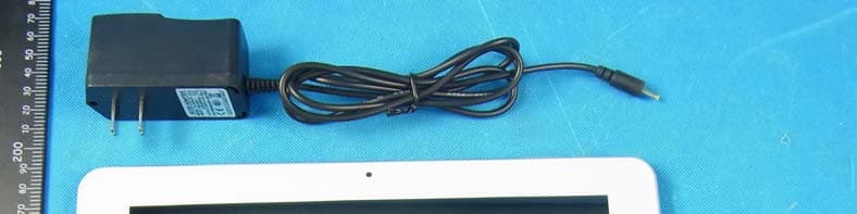
OX6VB100A
Sep 24, 2012Tablet PC
Equipment Class
DTS - Digital Transmission System
OX6VB736
Sep 23, 2012Tablet PC
Equipment Class
DTS - Digital Transmission SystemOX6VDD1010
Aug 13, 2012Digitizer Monitor
Equipment Class
JBC - Part 15 Class B Computing Device/Personal Computer