PJU2410-1Cordless Phone
Shenzhen Jingneng Telecom Technology Co Ltd
Click to zoom
Application Details
- Equipment Class
- DXX - Part 15 Low Power Communication Device Transmitter
- Date of Grant
- Feb 24, 2003
- Application Purpose
- Original Equipment
- Date of Application
- Feb 24, 2003
- Equipment Note
- Cordless Phone
- Frequency Range
- 2474.00000000 - 2476.45000000
- Country
- China
Documents & Files
Document Text
Text extracted from the exhibit documents filed with the FCC. Open a document above to read the original.
Users Manual
Southwestern BellFreedom Phone2.4GHzCORDLESS TELEPHONE GH2410C Owners ManualToll-Free Help Line 1-800-366-0937http://www.swbfredomphone.com R CID CH ERASE REV VOL EDIT SAVE PAUSE OPTION Southwestern B ell Freedom P hone R MUTE For immediate answers to your questions regarding operation missing parts or installation call: 1-800-366-0937 Monday - Friday 8:30 a.m.- 9:00 p.m. EST Saturday 8:30 a.m. - 12:30 p.m.EST http://www.swbfreedomphone.com 7475N.Glen Harbor Blvd Glendale AZ 85307 . - DON T TAKE ME BACK TO THE STORE. STOP - FOR THE TOLL - FREE HELP TELEPHONE NUMBER. LOOK - AS THE EXPERTS TALK YOU THROUGH THE PROBLEM. LISTEN Southwestern Bell Freedom Phone Help Line dt R SOUTHWESTERN BELL FREEDOMPHONE RETAIL SALES R GH2410C PrintedinChina IB-4142 1. Read and understand all instructions.2. Follow all warnings and instructions marked on the product.3. Use only with class 2 power source DC 9V 300mA.4. Unplug this product from the wall outlet before cleaning. Do not use liquid cleaners or aerosol cleaners. Use a damp cloth for cleaning. 5. Do not use this product near water; for example, near a bathtub, wash bowl, kitchen sink or laundry tub, in a wet basement or near a swimming pool. 6. Do not place this product on an unstable cart, stand, or table. The product may fall, causing serious damage to the Product. 7 . Slots and openings in the cabinet back or bottom are provided for ventilation. To protect it from overheating, these openings must not be blocked or covered. The openings should never be blocked by placing the product on the bed,sofa, rug, or other similar sur-face. This product should never be placed near or over a radiator or heat register. This productshould not be placed in an enclosed environment unless proper ventilation is provided. 8. Do not allow anything to rest on the power cord. Do not locate this product where the cord will be abused by animals or persons walking on it. 9. Do not overload wall outlets and extension cords as this can result in risk of fire or electrical shock.10. Never push objects of any kind into this product through cabinet slots as they may touch dangerous voltage points or short out parts that could result in a risk of fire or electrical shock. Never spill liquid of any kind on the product. 11. To reduce the risk of electrical shock, do not disassemble this product. Instead take it to a qualified service person when service or repair wor is required. Opening or removing covers may expose you to dangerous voltages or other risks.Incorrect re-assembly can cause electrical shock when the appliance is subsequently used. 12. Unplug all cords and refer servicing to qualified service personnel under the following conditions: A. When the power supply cord or plug is damaged or frayed.B. If liquid has been spilled into the product.C. If the product has been exposed to rain or water.D. If the product does not operate normally by following the operating instructions. Adjust only those controls covered in the operating instructions. Improper adjustment of other controls may result in damage and require work by a qualifiedtechnician to restore the product to normal operation. 13. Avoid using a telephone (other than a cordless type) during an electrical storm. There may be a remote risk of electric shock from lightning. 14. Do not use a telephone to report a gas leak in the vicinity of the leak.1. Use only the type and size of batteries specified in the users manual.2. Do not dispose of the batteries in a fire. The cells may explode. Check with local codes for possible special disposal instructions. 3. Do not open or mutilate the batteries. Released electrolyte is corrosive and may cause damage to the eyes or skin. It may be toxic if swallowed. 4. Exercise care in handling batteries in order not to short the battery with conducting materials such as rings, bracelets and keys. The battery or conductor may overheat and cause burns. 5 . Do not attempt to recharge the batteries with or identified for use with this product. The batteries may leak corrosive electrolyte or explode. 6. Do not attempt to rejuvenate the batteries provided with or identified for use with this product by heating them. Sudden release of the battery electrolyte may occur causing burns or irritation to eyes or skin. 7. When replacing batteries, all batteries should be replaced at the same time. Mixing fresh and discharged batteries could increase internal cell pressure and rupture the discharged batteries. 8. When inserting the batteries into this product, the proper polarity or direction must be observed. Reverse insertion of batteries can cause charging, which may result in leakage or explosion. 9. Remove the batteries from this product if the product will not be used for a long period of time (several months or more) since during this time the batteries could leak, damaging the product. 10. Discard "dead" batteries as soon as possible since they are more likely to leak in a product.11. Do not store this product, or the batteries provided with or for identified use with this product, in high temperature areas.12. If your product uses a rechargeable battery, charge the battery(ies) only in accordance with the instructions and limitation specified in the User Manual. This symbol is to alert you to important operating or servicing instructions that may appear in the user's manual. Always follow basic safety precautions when using this product to reduce the risk ofinjury, fire, or electrical shock. When using this product, basic safety precautions should always be followed to reduce the risk of fire, electric shockIF YOUR PRODUCT UTILIZES BATTERIES,THE FOLLOWING ADDITIONAL PRECAUTIONS SHOULD BE OBSERVED:And injury to persons, including the following: SAVE THESE INSTRUCTIONS Important Safety Instructions ...........2Battery Cautionary Instructions ........ 3Location of Controls and Features....5-9 .................................5-6 ..................... ................7-8 ......................…
Text truncated - open the document above for the full version.
External Photos
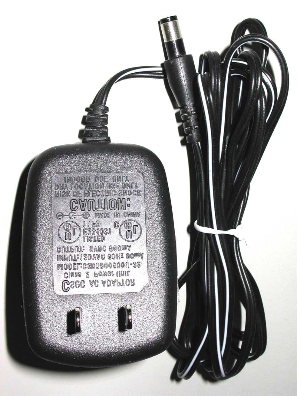
Shenzhen Jingneng Telecom Technology Co., Ltd. FCC ID: PJU2410-1 APPENDIX C - EUT EXTERNAL PHOTOGRAPHS Base – Top View Base – Bottom View Shenzhen Jingneng Telecom Technology Co., Ltd. FCC ID: PJU2410-1 Base – Port View Handset –Top View Shenzhen Jingneng Telecom Technology Co., Ltd. FCC ID: PJU2410-1 Handset – Bottom View Setup View Shenzhen Jingneng Telecom Technology Co., Ltd. FCC ID: PJU2410-1 Adapter – Top View
ID Label/Location Info
EXHIBIT A - FCC PRODUCT LABELING AND WARNING STATEMENT Proposed FCC ID Label Proposed ID Label for Base Proposed ID Label for Handset Specifications: Text is black or white in color and is left justified. Labels are silk-screened and shall be “permanently affixed” at a conspicuous location on the EUT. Proposed Label Location on EUT Bottom Side of EUT Base/Proposed FCC ID Label Location/Handset FCC Warning Statement A FCC Warning Statement is provided in the product manual. FCC ID: PJU2410-1
Internal Photos
Shenzhen Jingneng Telecom Technology Co., Ltd. FCC ID: PJU2410-1 APPENDIX C - EUT INTERNAL PHOTOGRAPHS Base – Motherboard Component View Base – Motherboard Solder View Shenzhen Jingneng Telecom Technology Co., Ltd. FCC ID: PJU2410-1 Base – Transceiver Component View Base – Transceiver Component Unshielded View Shenzhen Jingneng Telecom Technology Co., Ltd. FCC ID: PJU2410-1 Base – Transceiver Solder Unshielded View Handset – Motherboard Component View Shenzhen Jingneng Telecom Technology Co., Ltd. FCC ID: PJU2410-1 Handset – Motherboard Solder View Handset – Transceiver Component View Shenzhen Jingneng Telecom Technology Co., Ltd. FCC ID: PJU2410-1 Handset – Transceiver Solder View Handset – Transceiver Component Unshielded View Shenzhen Jingneng Telecom Technology Co., Ltd. FCC ID: PJU2410-1 Handset – Transceiver Solder Unshielded View
Operational Description
GH-2410 CIRCUIT DESCRIPTION BASE UNIT : The demodulated signal, resulting from Double Super Heterodyne system, which appears at output Pin no.3 of J 3 is sent to IC2 (COMPANDER IC) Pin no.16 for Expansion. The expended audio signal output from Pin no.19 is coupled to Q8,the audio signal is sent to the Telephone Line through Q3.. The demodulated data code from J3 Pin no.3 is Generated by IC-324.. It’s output is connected to CODE Input Pin no.31 of IC4 The Audio signal receiving from TEL-LINE is input to IC2 Pin no.8 for compression. The compressed audio signal from Pin no.1 of IC2 is connected to Pin no.10 of J3 for TX modulation. Pin no.21 of IC4 is the output port for data codes that should be transmitted to the handset the data code is connected to Pin no.10 of J3 for modulation. Line controlling is done by Pin no.10 of IC4. Ring signal monitored by IC7 (PHOTO COUPLER IC) is detected by Pin no.9 of IC4 resulting a data code to the handset. DTMF dialing is generated by IC4 Pin no.38 this signal output through the Q4.Q3. When the handset is placed on the base cradle, the charging is detected by Pin no.8 of IC4 and IC4 sends data codes to handset for security code setting. When the handset is far away form base unit, squelch circuit of IC4 operates and Pin no.30 of IC4 goes “HI”. This will be detected by the micro processor and after 20 sec. go to Stand by mode. The power to the base unit is supplied by IC5(5V REGULATOR IC). LED display control Pin no.22 of IC4. HAND SET : The demodulated signal, resulting from Double Super Heterodyne system, which appears at output Pin no.3 of CON1 is connected to U2-B Pin no.16 Expander input. The audio output from U2-B Pin no.19 is finally amplified by Q8 and A.C coupled to the Receiver unit with HAC compatibility. The demodulated data code from CON1 Pin no.3 is fed to Q9,10. Q9 is connected to (DATA IN) Pin no.26 of U1. Voice signal from C-MIC is coupled to Pin no.8 of IC-PH1. The voice signal is compressed by U2 and output Pin no.1 is connected to Pin no.10 of CON1 for modulation. Pin no.29 of U1 is the output port for data code that should be transmitted to the base unit. This data code is connected to the Pin no.10 of CON1 for modulation. During the charging, it is detected by U1 Pin no.23. Key board operation is monitored by Pin no.50~ 61of U1. Key Tone and the ringing from Pin no.62 of U1 drives the BUZZER. 1. BASE RF MODULE 1) RX PART THE RECEIVER FRONT-END CONTAINS A BAND PASS FILTER, AND RF LOW NOISE AMPLIFIER, A ACTIVE TRANSISTOR MIXER, A CERAMIC FILTER AND 10.7MHz IF AMPLIFIER. ALSO IT INCLUDES BUFFER AMPLIFIERS FOR THE GENERATION OF LOCAL OSCILLATOR POWER. THIS FRONT-END RECEIVER RECEIVERS AND RF SIGNAL FROM THE ANTENNA. AND RF SIGNALS WITHIN THIS FREQUENCY RANGE IS 2403.05MHz ~ 2475.95MHz PASS THROUGH RF AMP (Q1) AND BAND PASS FITER. AFTER PASSING THROUGH THE BAND PASS FILTER AND THE SIGNAL IS MIXED WITHIN 1’ST LOCAL FREQUENCY FROM VOLTAGE CONTROLLED OSCILLATOR. THE SIGNAL IS AMPLIFIED ON THE OF AMP TRANSISTOR (Q3) AND THE SIGNAL PASS THROUGH THE CERAMIC FILTER (10.7MHz). AFTER THE IF SIGNAL PASS THE CERAMIC FILTER, THE SIGNAL ENTER BY THE FM IF(INTERMEDIATE FREQUENCY) IC1. AND THE SIGNAL IS MIXED IN THE FM IF IC (DBL5018V). THE SIGNAL PASS THROUGH THE CERAMIC FILTER (450KHz). THE OUTPUT SIGNAL IN THE FM IF IC STREAMS FROM THE AF-OUT TERMINAL OF THE CONNECTOR TO THE BASE. FIG. 1 ANTENNA IC 1 AF-OUT BPF F1 LNA Q1 VCO MIXER 1’ST LOCAL FREQUENCY F2 10.7MHz IF IC DBL5018 GND 450KHz 2’nd LOCAL FREQ. TCXO 11.15MHz 2)TX PART THE SIGNAL IS MADE TO THE BASE, ENTER BY THE AF-IN TERMINAL OF THE CONNECTOR(CON1 OF PIN NO.10). THE SIGNAL SEND THE MOD TERMINAL OF THE TX VCO. THE SIGNAL IS MIXED IN THE TX VCO MIXING THE RF SIGNAL, THE RF SIGNAL ADJUST THE TRIMMER CAPACITOR (VC1). THE RF SIGNAL ENTER BY THE TRANSMISSION POWER AMP TRANSISTOR Q4 THE SINAL IS AMPLITUDE IN THE Q5. ENTER BY THE BAND PASS FILTER. THE RF SIGNAL PASS THROUGH THE BAND PASS FILTER, TO WARDS THE ANT. THE LAST TRANSMISSION RF SIGNAL IS 2403.05MHz ~ 2475.95MHz. FIG. 2 RF MODULE AF-IN VCO BPF3 2403MHz ANTENNA PLL IC IC2 Q5,4 TCXO 11.15MHz TREMMER CAP. VC1 2. PORTABLE RF MODULE 1) RX RART THE RECEIVER FRONT-END CONTAINS A BAND PASS FILTER,AND RF LOW NOISE AMPLIFIER, ACTIVE TRANSISTOR MIXER, CERAMIC FILTER AND 10.7MHz “IF” AMPLIFTER. ALSO IT INCLUDES BUFFER AMPLIFIERS OR THE GENERATION OF LOCAL OSCILLATOR POWER. THIS FRONT-END RECEIVERS AND RF SIGNAL FROM THE ANTENNA. AND RF SIGNALS WITHIN THIS FREQUENCY RANGE IS 2403.05MHz ~ 2475.95MHz PASS THROUGH RF AMP (Q1) AND BAND PASS FILTER.. AFTER PASSING THROUGH THE BAND PASS FILTER, THE SIGNAL IS MIXED WITHIN 1’ST LOCAL FREQUENCY FROM VOLTAGE CONTROLLED OSCILLATOR. THE SIGNAL IS AMPLIFIED ON THE IF AMP TRANSISTOR (Q3) AND THE SIGNAL PASS THROUGH THE CERANIC FILTER (10.7MHz) AFTER THE IF SIGNAL PASS THE MCF FILTER, THE SIGNAL ENTER BY THE FM IF (INTERMEDIATE FREQUENCY) IC. AND THE SIGNAL IS MIXED IN THE FM IF IC (DBL5018V). THE SIGNAL PASS THROUGH THE CERAMIC FILTER (450KHz). THE OUTPUT SIGNAL IN THE FM IF IC STREAMS FROM THE AF-OUT TERMINAL OF THE CONNECTOR 1 TO THE PORTABLE. FIG.3 ANTENNA IF IC DBL5018 F1 10. 7MHz IC 1 AF-OUT BPF F1 LNA Q1 VCO MIXER 1’ST LOCAL FREQUENCY 450KHz 2’nd LOCAL FREQ. TCXO 11.15MHz 2) TX PART THE SIGNAL IS MADE TO THE PORTABLE, ENTER BY THE AF-IN TERMINAL OF THE CONNECTOR. THE SIGNAL SEND THE MOD TERMINAL OF THE TX VCO. THE SIGNAL IS MIXED IN THE TX VCO MIXING THE RF SIGNAL, THE RF SIGNAL ADJUST THE TRIMMER CAPACITOR VC1. THE RF SIGNAL ENTER BY THE TRANSMISSION POWER AMP TRANSISTOR (Q5,7). ENTER BY THE BAND PASS FILTER. THE RF SIGNAL PASS THROUGH THE BAND PASS FILTER, TO WARDS THE ANT. THE LAST TRANSMISSION RF SIGNAL IS 2403.025MHz ~ 2475.95MHz. FIG. 4 RF MODULE AF-IN VCO TCXO 11.15MHz TREMMER CAP. VC1 Q5,7 F4 2475MHz ANTHNNA PLL IC IC2
Operational Description
<HANDY><BASE> Ch Tx(Mhz)Tx_Vco(Mhz) Rx(Mhz)Rx_Vco(Mhz)Tx(Mhz)Tx_Vco(Mhz) Rx(Mhz)Rx_Vco(Mhz) 1 2,474.000824.6666667 2402.55797.2832402.55797.283 2,474.000824.6666667 2 2,474.050824.6833333 2402.6797.3002402.6797.300 2,474.050824.6833333 3 2,474.100824.7 2402.65797.3172402.65797.317 2,474.100824.7 4 2,474.150824.7166667 2402.7797.3332402.7797.333 2,474.150824.7166667 5 2,474.200824.7333333 2402.75797.3502402.75797.350 2,474.200824.7333333 6 2,474.250824.75 2402.8797.3672402.8797.367 2,474.250824.75 7 2,474.300824.7666667 2402.85797.3832402.85797.383 2,474.300824.7666667 8 2,474.350824.7833333 2402.9797.4002402.9797.400 2,474.350824.7833333 9 2,474.400824.8 2402.95797.4172402.95797.417 2,474.400824.8 10 2,474.450824.8166667 2403797.4332403797.433 2,474.450824.8166667 11 2,474.500824.8333333 2403.05797.4502403.05797.450 2,474.500824.8333333 12 2,474.550824.85 2403.1797.4672403.1797.467 2,474.550824.85 13 2,474.600824.8666667 2403.15797.4832403.15797.483 2,474.600824.8666667 14 2,474.650824.8833333 2403.2797.5002403.2797.500 2,474.650824.8833333 15 2,474.700824.9 2403.25797.5172403.25797.517 2,474.700824.9 16 2,474.750824.9166667 2403.3797.5332403.3797.533 2,474.750824.9166667 17 2,474.800824.9333333 2403.35797.5502403.35797.550 2,474.800824.9333333 18 2,474.850824.95 2403.4797.5672403.4797.567 2,474.850824.95 19 2,474.900824.9666667 2403.45797.5832403.45797.583 2,474.900824.9666667 20 2,474.950824.9833333 2403.5797.6002403.5797.600 2,474.950824.9833333 21 2,475.000825 2403.55797.6172403.55797.617 2,475.000825 22 2,475.050825.0166667 2403.6797.6332403.6797.633 2,475.050825.0166667 23 2,475.100825.0333333 2403.65797.6502403.65797.650 2,475.100825.0333333 24 2,475.150825.05 2403.7797.6672403.7797.667 2,475.150825.05 25 2,475.200825.0666667 2403.75797.6832403.75797.683 2,475.200825.0666667 26 2,475.250825.0833333 2403.8797.7002403.8797.700 2,475.250825.0833333 27 2,475.300825.1 2403.85797.7172403.85797.717 2,475.300825.1 28 2,475.350825.1166667 2403.9797.7332403.9797.733 2,475.350825.1166667 29 2,475.400825.1333333 2403.95797.7502403.95797.750 2,475.400825.1333333 30 2,475.450825.15 2404797.7672404797.767 2,475.450825.15 31 2,475.500825.1666667 2404.05797.7832404.05797.783 2,475.500825.1666667 32 2,475.550825.1833333 2404.1797.8002404.1797.800 2,475.550825.1833333 33 2,475.600825.2 2404.15797.8172404.15797.817 2,475.600825.2 34 2,475.650825.2166667 2404.2797.8332404.2797.833 2,475.650825.2166667 35 2,475.700825.2333333 2404.25797.8502404.25797.850 2,475.700825.2333333 36 2,475.750825.25 2404.3797.8672404.3797.867 2,475.750825.25 37 2,475.800825.2666667 2404.35797.8832404.35797.883 2,475.800825.2666667 38 2,475.850825.2833333 2404.4797.9002404.4797.900 2,475.850825.2833333 39 2,475.900825.3 2404.45797.9172404.45797.917 2,475.900825.3 40 2,475.950825.3166667 2404.5797.9332404.5797.933 2,475.950825.3166667 41 2,476.000825.3333333 2404.55797.9502404.55797.950 2,476.000825.3333333 42 2,476.050825.35 2404.6797.9672404.6797.967 2,476.050825.35 43 2,476.100825.3666667 2404.65797.9832404.65797.983 2,476.100825.3666667 44 2,476.150825.3833333 2404.7798.0002404.7798.000 2,476.150825.3833333 45 2,476.200825.4 2404.75798.0172404.75798.017 2,476.200825.4 46 2,476.250825.4166667 2404.8798.0332404.8798.033 2,476.250825.4166667 47 2,476.300825.4333333 2404.85798.0502404.85798.050 2,476.300825.4333333 48 2,476.350825.45 2404.9798.0672404.9798.067 2,476.350825.45 49 2,476.400825.4666667 2404.95798.0832404.95798.083 2,476.400825.4666667 50 2,476.450825.4833333 2405798.1002405798.100 2,476.450825.4833333 Table2-4. LMX1602 CLP DUAL PLL FREQ 1
Schematics
2410VS-BM.sch-1 - Tue Feb 25 10:02:33 2003
Schematics
2410VS-HM.sch-1 - Tue Feb 25 10:05:33 2003
Test Report
Note: This test report is specially limited to the above client company and the product model only. It may not be duplicated without prior written consent of Bay Area Compliance Laboratory Corporation. This report must not be used by the client to claim product endorsement by NVLAP or any agency of the U.S. Government. FCC PART 15 SUBPART C EMI MEASUREMENT AND TEST REPORT For Shenzhen Jingneng Telecom Technology Co., Ltd. Baimenqian Industrial Zone, Shawan, Buji Town, Longgang District, Shenzhen City, P.R.China FCC ID: PJU2410-1 February 5, 2003 This Report Concerns: Original Report Equipment Type: Cordless Telephone Test Engineer:Benjamin Jing Report No.:R0301217 Test Date:January 23, 2003 Reviewed By:Hans Mellberg Prepared By:Bay Area Compliance Laboratory Corporation 230 Commercial Street Sunnyvale, CA 94085 Tel (408) 732-9162 Fax (408) 732-9164 Shenzhen Jingneng Telecom Technology Co., Ltd. FCC ID: PJU2410-1 Report # R0301217RptPage 2 of 16FCC Part 15 Subpart C Test Report TABLE OF CONTENTS 1 - GENERAL INFORMATION.................................................................................................................................................3 1.1 PRODUCT DESCRIPTION FOR EQUIPMENT UNDER TEST (EUT).........................................................................................3 1.2 OBJECTIVE................................................................................................................................................................................3 1.3 RELATED SUBMITTAL(S)/GRANT(S)......................................................................................................................................3 1.4 TEST METHODOLOGY.............................................................................................................................................................3 1.5 TEST FACILITY.........................................................................................................................................................................3 1.6 TEST EQUIPMENT LIST............................................................................................................................................................4 1.8 LOCAL SUPPORT EQUIPMENT LIST AND DETAILS...............................................................................................................4 1.9 EXTERNAL I/O CABLING LIST AND DETAILS......................................................................................................................4 2 - SYSTEM TEST CONFIGURATION..................................................................................................................................5 2.1 DESCRIPTION OF TEST CONFIGURATION..............................................................................................................................5 2.2 CONFIGURATION OF TEST SYSTEM (BASE).........................................................................................................................6 2.3 TEST SETUP BLOCK DIAGRAM..............................................................................................................................................6 3 - CONDUCTED EMISSION.....................................................................................................................................................7 3.1 MEASUREMENT UNCERTAINTY.............................................................................................................................................7 3.2 EUT SETUP...............................................................................................................................................................................7 3.3 SPECTRUM ANALYZER SETUP...............................................................................................................................................7 3.4 TEST PROCEDURE....................................................................................................................................................................7 3.5 SUMMARY OF TEST RESULTS.................................................................................................................................................8 3.6 CONDUCTED EMISSIONS TEST DATA....................................................................................................................................8 3.7 PLOT OF CONDUCTED EMISSIONS TEST DATA....................................................................................................................8 4 - RADIATED EMISSION........................................................................................................................................................11 4.1 MEASUREMENT UNCERTAINTY...........................................................................................................................................11 4.2 EUT SETUP.............................................................................................................................................................................11 4.3 SPECTRUM ANALYZER SETUP.............................................................................................................................................11 4.4 TEST PROCEDURE..................................................................................................................................................................12 4.5 CORRECTED AMPLITUDE & MARGIN CALCULATION......................................................................................................12 4.6 SUMMARY OF TEST RESULTS...............................................................................................................................................12 4.7 RADIATED EMISSIONS TEST RESULT DATA......................................................................................................................13 5 - BAND EDGES................…
Text truncated - open the document above for the full version.
Test Setup Photos
Shenzhen Jingneng Telecom Technology Co., Ltd. FCC ID: PJU2410-1 Base Conducted Emission - Front View Base Conducted Emission - Rear View Shenzhen Jingneng Telecom Technology Co., Ltd. FCC ID: PJU2410-1 Base Radiated Emission - Front View Base Radiated Emission - Rear View Shenzhen Jingneng Telecom Technology Co., Ltd. FCC ID: PJU2410-1 Handset Radiated Emission - Front View Handset Radiated Emission - Rear View
Contact Information
Applicant
Zheng Caian(QA Manager)
Test Firm
Bay Area Compliance LaboratoryJohn Chan
Technical Specifications
| # | Rule Parts | Frequency Range | Power Output |
|---|---|---|---|
| 2 | 15C | 2.47 GHz - 2.48 GHz | - |
Other Applications from Shenzhen Jingneng Telecom Technology Co Ltd
PJUGH9492
Jun 01, 20042.4G ANALOG CORDLESS PHONE WITH CID AND DAM
Equipment Class
DXX - Part 15 Low Power Communication Device Transmitter
PJU2400-01
Mar 18, 20032.4 GHz Cordless Telephone
Equipment Class
DXX - Part 15 Low Power Communication Device Transmitter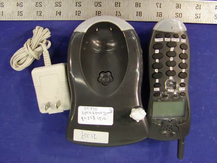
PJUHK250
Oct 24, 2002Cordless Telephone Base and Handset
Equipment Class
DXX - Part 15 Low Power Communication Device Transmitter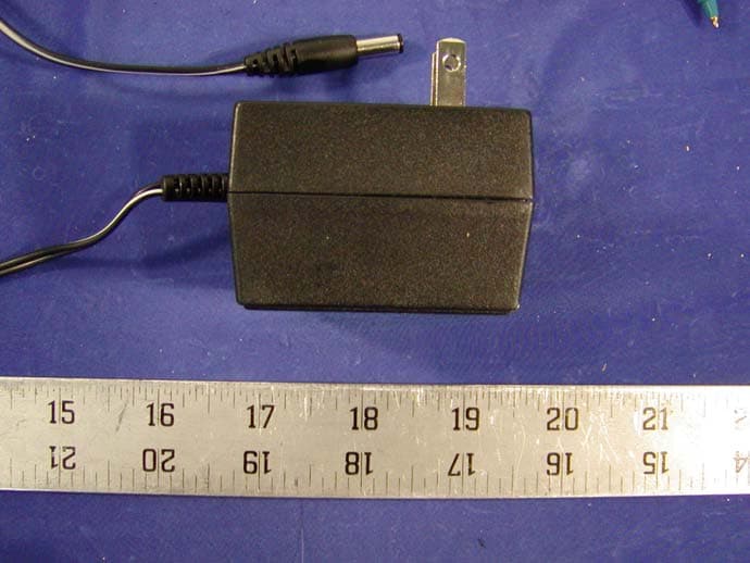
PJUGH3050
Jul 14, 20022.4GHz Cordless Phone
Equipment Class
DXT - Part 15 Low Power Transceiver, Rx Verified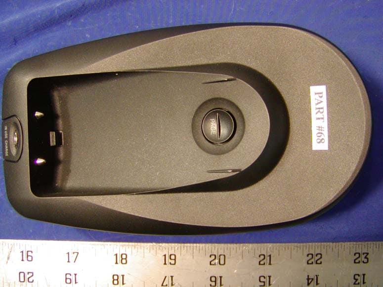
PJUTC970
May 20, 20022.4GHz Cordless Phone
Equipment Class
DXX - Part 15 Low Power Communication Device Transmitter