PM3GX90Transceiver, UHF, PTT
Genex Telecom Co., Ltd.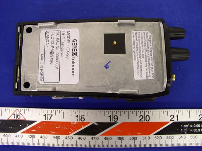
Click to zoom
Application Details
- Equipment Class
- TNF - Licensed Non-Broadcast Transmitter Held to Face
- Date of Grant
- Apr 05, 2004
- Application Purpose
- Original Equipment
- Date of Application
- Apr 05, 2004
- Equipment Note
- Transceiver, UHF, PTT
- Frequency Range
- 430.00000000 - 470.00000000
- Company
- Genex Telecom Co., Ltd.
- Country
- South Korea
Documents & Files
Document Text
Text extracted from the exhibit documents filed with the FCC. Open a document above to read the original.
Users Manual
GX-80/90 Genex Portable LMR radio FCC RF EXPOSURE COMPLIANCE REQUIREMENTS FOR OCCUPATIONAL USE ONLY The Federal Communications Commission (FCC), with its action in General Docket 93-62, November 7, 1997, has adopted a safety standard for human exposure to Radio Frequency (RF) electromagnetic energy emitted by FCC regulated equipment. Maxon subscribes to the same safety standard for the use of its products. Proper operation of this radio will result in user exposure far below the Occupational Safety and Health Act (OSHA) and Federal Communications Commission limits. DO NOT transmit for more than 50% of total radio use time (50% duty cycle). Transmitting more than 50% of the time can cause FCC RF exposure compliance requirements to be exceeded. •This radio is NOT approved for use by the general population in an uncontrolled environment. This radio is restricted to occupational use, work related operations only where radio operator must have the knowledge to control the user’s exposure conditions for satisfying the higher exposure limit allowed for occupational use. •When transmitting, hold the radio in a vertical position with its microphone 2 inches (5 cm) away from your mouth. The radio is transmitting when the red LED on the front of the radio is illuminated. You can cause the radio to transmit by pressing the PTT bar on the radio. These are required operating configurations for meeting FCC RF exposure compliance. Failure to observe these restrictions mean violation. This equipment complies with the FCC RF Exposure Limits for controlled environments. - Function description 1. power on& volume control (1) Power On Turn radio on by turning the power/volume Rotary switch clockwise out of detent. When radio turns on, it make beep sound. (2) Power Off Turning the power /volume rotary switch counterclockwise out of detent (3) Volume up/down Adjusting level of volume by turning Volume rotary switch. 2. Channel Selecting (Up/Down) User can choose a channel by adjusting Channel rotary switch 3. RX Operation 1) Busy condition is that unit is receiving a signal fixed in its channel Unit in the busy condition will be operated according to a fixed input of tone and two Tone. Unit out of busy condition will remain LED Off 2) Correct Call If a incoming signal has same tone as a fixed input of tone in selected channel, This signal is called “Correct Unit will open Audio with Green LED, If a incoming signal is not correct call, LED will be On in orange. 3) Monitor Operation Whenever Monitor button is pressed, Audio must be opened regardless of the condition of busy or correct call. - Monitor On : press Monitor button in left side of radio, Audio will be opened. If press Monitor button for five seconds, Monitor button will be locked and then a opened audio will be maintained, even though user release monitor button. If user release monitor button within five seconds, Monitor function will be Off and then Audio will be controlled by a incoming signal. To be out of Monitor condition, Just press monitor again. 4) Scan operation - Normal scan On : Press Sacn Button on the left side of radio for two seconds, User can initiate scan with beep sound. If no conversation is detected on any channel in the scan list, Radio will make Error beep sound, Once Scan starts, LED will flash in order of the following step repeatedly as below RED ==Î GREED ===Î Orange It indicates that Scan is on progress. To stop scanning, Press Scan button again for a two seconds, Radio will go back to the original channel used before start a scan and then radio stops flashing LED. If a conversation is detected a correct call, radio will stop on that channel and user will be able to hear the conversation. If programmed for normal scan TX, you will be able to transmit on that active channel during the programmable scan delay time. The scan delay time is the amount of time. Radio will stay on that channel once activity has cased. The radio will resume scanning once the scan delay time has expired. Scanning will continue until the channel is changed or press scan button again. - Scan channel Delete : To temporarily delete a channel from the scan list, simply press the scan button for a short time while stopped on the channel to be detected. This will remove that channel from the scan list until the channel is changed or the radio’s power is reset. When power is restored or the scan list channel position is again selected, the original dealer programmed scan list will be activated. - Priority Scan On : A single channel is programmed as the “ Priority” channel. The radio will constantly monitor this channel with flashing LED while scanning and when the radio has stopped on an active channel. If a call is detected on the “priority” channel, the radio will automatically move to, and remain on the “ Priority” channel as long as the priority conversation takes places. “priority” channel activity takes precedence over all other conversations. - Priority Scan Off : To be out of “Priority scan” Just change Channel. Radio will stop for a programmed delay time and start scanning on priority scan option activity channel. - Look back (Receiving correct call in Priority scan mode) Any channel, when not in the scan mode can be programmed to “look back” at the priority channel. This feature is ideal for those who do not need scan as defined above, but want to make sure that they never miss a call on the “priority” channel if another channel has been selected, the radio will periodically “look back” at the Priority channel. If activity is detected on the “priority” channel, the radio will move to that channel for as long as it remains active. - Priority Scan TX : If a coming signal is not correct call, allow transmission on the normal channel. If a coming signal is a correct call, allow transmission on the correct call channel. After finish transmission, resume scan after scan delay time. - Muti Scan : if press Scan key while Priority scan mode is On, Priority…
Text truncated - open the document above for the full version.
Users Manual
GX-80/90 Genex Portable LMR radio FCC RF EXPOSURE COMPLIANCE REQUIREMENTS FOR OCCUPATIONAL USE ONLY The Federal Communications Commission (FCC), with its action in General Docket 93- 62, November 7, 1997, has adopted a safety standard for human exposure to Radio Frequency (RF) electromagnetic energy emitted by FCC regulated equipment. Maxon subscribes to the same safety standard for the use of its products. Proper operation of this radio will result in user exposure far below the Occupational Safety and Health Act (OSHA) and Federal Communications Commission limits. •This radio is NOT approved for use by the general population in an uncontrolled environment. This radio is restricted to occupational use, work related operations only where radio operator must have the knowledge to control the user’s exposure conditions for satisfying the higher exposure limit allowed for occupational use. •When transmitting, hold the radio in a vertical position with its microphone 2 inches (5 cm) away from your mouth. The radio is transmitting when the red LED on the front of the radio is illuminated. You can cause the radio to transmit by pressing the PTT bar on the radio or, if in VOX mode, by simply talking above the threshold level set during VOX programming. DO NOT transmit either in PTT or VOX mode for more than 50% of total radio use time (50% duty cycle). Transmitting more than 50% of the time can cause FCC RF exposure compliance requirements to be exceeded. These are required operating configurations for meeting FCC RF exposure compliance. Failure to observe these restrictions mean violation. This equipment complies with the FCC RF Exposure Limits for controlled environments. - Function description 1. power on& volume control (1) Power On Turn radio on by turning the power/volume Rotary switch clockwise out of detent. When radio turns on, it make beep sound. (2) Power Off Turning the power /volume rotary switch counterclockwise out of detent (3) Volume up/down Adjusting level of volume by turning Volume rotary switch. 2. Channel Selecting (Up/Down) User can choose a channel by adjusting Channel rotary switch 3. RX Operation 1) Busy condition is that unit is receiving a signal fixed in its channel Unit in the busy condition will be operated according to a fixed input of tone and two Tone. Unit out of busy condition will remain LED Off 2) Correct Call If a incoming signal has same tone as a fixed input of tone in selected channel, This signal is called “Correct Unit will open Audio with Green LED, If a incoming signal is not correct call, LED will be On in orange. 3) Monitor Operation Whenever Monitor button is pressed, Audio must be opened regardless of the condition of busy or correct call. - Monitor On : press Monitor button in left side of radio, Audio will be opened. If press Monitor button for five seconds, Monitor button will be locked and then a opened audio will be maintained, even though user release monitor button. If user release monitor button within five seconds, Monitor function will be Off and then Audio will be controlled by a incoming signal. To be out of Monitor condition, Just press monitor again. 4) Scan operation - Normal scan On : Press Sacn Button on the left side of radio for two seconds, User can initiate scan with beep sound. If no conversation is detected on any channel in the scan list, Radio will make Error beep sound, Once Scan starts, LED will flash in order of the following step repeatedly as below RED == Î GREED === Î Orange It indicates that Scan is on progress. To stop scanning, Press Scan button again for a two seconds, Radio will go back to the original channel used before start a scan and then radio stops flashing LED. If a conversation is detected a correct call, radio will stop on that channel and user will be able to hear the conversation. If programmed for normal scan TX, you will be able to transmit on that active channel during the programmable scan delay time. The scan delay time is the amount of time. Radio will stay on that channel once activity has cased. The radio will resume scanning once the scan delay time has expired. Scanning will continue until the channel is changed or press scan button again. - Scan channel Delete : To temporarily delete a channel from the scan list, simply press the scan button for a short time while stopped on the channel to be detected. This will remove that channel from the scan list until the channel is changed or the radio ’ s power is reset. When power is restored or the scan list channel position is again selected, the original dealer programmed scan list will be activated. - Priority Scan On : A single channel is programmed as the “ Priority ” channel. The radio will constantly monitor this channel with flashing LED while scanning and when the radio has stopped on an active channel. If a call is detected on the “priority” channel, the radio will automatically move to, and remain on the “ Priority ” channel as long as the priority conversation takes places. “ priority ” channel activity takes precedence over all other conversations. - Priority Scan Off : To be out of “ Priority scan ” Just change Channel. Radio will stop for a programmed delay time and start scanning on priority scan option activity channel. - Look back (Receiving correct call in Priority scan mode) Any channel, when not in the scan mode can be programmed to “ look back ” at the priority channel. This feature is ideal for those who do not need scan as defined above, but want to make sure that they never miss a call on the “ priority ” channel if another channel has been selected, the radio will periodically “ look back ” at the Priority channel. If activity is detected on the “priority” channel, the radio will move to that channel for as long as it remains active. - Priority Scan TX : If a coming signal is not correct call, allow transmission on the normal channel. If a coming signal is a correct call, allow transmission on the correct call channel. …
Text truncated - open the document above for the full version.
External Photos
GENEX Telecom CO., LTD. FCC ID: PM3GX90 APPENDIX C - EUT PHOTOGRAPHS Chassis - Front View Chassis – Back View I GENEX Telecom CO., LTD. FCC ID: PM3GX90 Chassis – Back View II Chassis – Back Frame GENEX Telecom CO., LTD. FCC ID: PM3GX90 Chassis – Top View Chassis – Bottom View GENEX Telecom CO., LTD. FCC ID: PM3GX90 Chassis – Left Side View Chassis – Right Side View GENEX Telecom CO., LTD. FCC ID: PM3GX90 Adapter View Battery Charger – Front View GENEX Telecom CO., LTD. FCC ID: PM3GX90 Battery Charger – Rear View
ID Label/Location Info
APPENDIX A - FCC ID LABELING AND LOCATION Proposed FCC ID Labeling Proposed FCC ID Location Rear Side of EUT / Proposed Label Location FCC ID: PM3GX90
ID Label/Location Info
APPENDIX A - FCC ID LABELING AND LOCATION Proposed FCC ID Labeling Proposed RF Safety Labeling Proposed Label Location Back Frame View of EUT / Proposed Label Location FCC ID: PM3GX90 This device must be restricted to occupational use to satisfy FCC RF exposure compliance. See owner’s manual for specific operating instruction. This device must be restricted to occupational use to satisfy FCC RF exposure compliance. See owner's manual for specific operating instruction.
Internal Photos
GENEX Telecom CO., LTD. FCC ID: PM3GX90 Battery Charger – Cover off View GENEX Telecom CO., LTD. FCC ID: PM3GX90 Battery Charger – Component View Battery Charger – Solder View GENEX Telecom CO., LTD. FCC ID: PM3GX90 PCB – Top View I PCB – Top View II GENEX Telecom CO., LTD. FCC ID: PM3GX90 PCB – Bottom View
Operational Description
THEORY OF OPERATION Theory of Operation on GX Series The GX Series Handheld Radio Transceivers are comprised of one main PCB. The main PCB contains the transmitter, receiver, and control circuits. Receiver The receiver circuit adopts dual conversion super heterodyne with 1 st IF 45.1MHz and 2 nd IF 455kHz Front-end Front-end consists of pre-selector filter, RF Amplifier, Post-selector filter. The receive signal is routed through C3 and selected by C4, C6, L2, L3 to amplified around 13dB at RF amp. Q19. Front-end adjusts bandwidth by varicap diode tuning. This circuit removes unnecessarily spurious 1st Image. First Mixer The signal from Front-end is input to Q18 base of 1 st mixer. 1 st local signal generated from VCO is input to Q18, emitter. These two signals are mixed at Mixer into 1 st IF signal 45.1MHz, which is resonated in parallel at C22, L8 and inputted to XF1, Pair crystal filter. IF Amplifier 1 st IF signal from XF1 is amplified about 15dB at IF amp Q17 and inputted to IC3, IF IC. 2 nd Local Oscillator is 44.645MHz. The signal from 2 nd Mixer is refined removing unnecessary spurious signal and detected through high gain linear amp. This detected signal is inputted to IC3 pin9. AF Amplifier 300Hz High Pass Filter IC507 removes the signal under 300Hz of the demodulated signal from IC3 so that noise under sub tone use is removed. De-emphasis functions to get 6dB/oct by R601, C533 and this signal controls volume of sound by RV502. IC508 can operate a speaker as audio current amplifier amplifying the signal. The operating current can be reduced by mute signal. Squelch The demodulated signal from IC3 is coupled of noise to C35. The noise is filtered and amplified by C45,109, R30 and used internal amplifier of IC3. This noise signal is used as the signal to mute RV2 audio. Audio AMP After CTCSS,DCS signal is removed at 300Hz High Pass Filter and de-emphasized to – 6 dB/Oct at R601, C533 the volume of sound is controlled by RV502. IC508 is doing low frequency current amplify as audio amplifier to operate a speaker. IC508 has mute function and if Pin 2, mute port is high, it's on mute. If it is low, it's unmuted. Transmitter The transmitter consists of Buffer, Power Amplifier, Low-Pass Filter, Antenna Switch, Auto-Power Control. 2-1) Buffer -6dBm TX RF signal from VCO is amplified to around +29dBm by buffer Q22,26 to have desired output power at final Amp. Pie style resister attenuator is used between VCO and Buffer Amp. To minimize the effect of load caused by transmit amplifier in TX. 2-2) Power Amplifier TX RF Signal form buffer Amp. Gains 6Watt output by final Amp Q27. Collect impedance of Q27 states in low so that it is matching to 50ohm by C97, 98, 99, 100, strip line and inputted to 5 th Low Pass Filter. 2-3) Low Pass Filter 5 th Low Pass Filter reduces the unwanted spurious for TX output power from final Amp. L19, 20, C103, 104, 105, 106, 107 are Chebisheve Filter. 2-4) Antenna Switch Ant. Switch is to share the antenna in TX and RX. It prevents TX sensitivity from degradation by LPF. Also, it protects receive circuit by blocking TX signal to receive end, turning on D1, 2. Flow of the signal in RX is designed to minimize the loss of the signal using the character of series resonance of L1, C3. 2-5) Auto-Power Control This circuit controls TX Power by detection on the current through R95. The voltage difference from these resistors is amplified by IC4-B and gets the voltage comparing the this signal with the reference voltage from R84, 85 at IC4-A. This voltage difference is kept to stable value by RV4 changing Gate voltage of Final Amp. PLL Synthesizer Reference frequency is 12.8MHz and this oscillated frequency is compensated in temperature. The frequency from VCO is inputted to PLL IC and this inputted signal is divided by the ratio set by data and compared with reference step frequency. Then, the difference comes to IC1 pin15,16 Port. GX series consists of external charge pump. Charge pump output turns into DC by PLL LPF R56, 57, 58, C59, 60, 61, 62 so that it can vary VCO control voltage to have set frequency. For TX and RX switch, Q305 and Q3304 base switch to control voltage.(TX_EN) Audio and Control circuit IC501 controls all factions of the radio as Microprocessor. It detects outer condition such as function data on frequency, Power supply switching and make it operate correctly. IC509 consists of 250Hz LPF to function CTCSS,DCS decoding correctly and he output of this filter is amplified at IC509- A. Then, it goes to Q503 to be changed to logic signal so that CTCSS,DCS decoding is enabled. IC509-A is CTCSS,DCS Encode Filter. It mixes the signals from 4 ports and this mixed signal goes through this filter to get clear CTCSS,DCS signal. IC509-B, C, and D is TX Audio Amp and limiter. It amplifies the voice signal from C-Mic and have the character of 6dB/Oct Pre-Emphasis. This voice signal is controlled by RV501 for the volume. IC509-B is 3KHz LPF and has the character that reduces to 18dB/Oct. This character minimizes the interference of adjacent channel by voice signal. Alignment Procedure This radio is adjusted to meet all condition in production except special case. Readjustment is not requirement. 5-1) The preparation before adjustment. 1) Set the Power Supply voltage to 7.4V and then connect to the radio. 2) Connect the connector to Radio Antenna terminal. 3) Connect the radio to test equipment. 5-2) PLL Synthesizer 1) Measure the voltage of TP1 with High impedance voltage meter. 2) Adjust TC301 at RX channel 1.0 to be 1.5V. Confirm if it is below 13V at RX high channel. Adjust TC302 at TX channel 1.0 to be 1.5V. Confirm if it is below 13V at TX high channel. 3) Confirm if Channel 1 is in 1.0 +/-0.3 in TX. 5-3) Adjustment of Transmitter 1) Adjust to tune the set frequency. 2) Adjust RV4 to tune the set power. 3) Set Audio Generator to be 1kHz 120mVrms and connect to Radio External Jack. 4) Adjust RV501 to tune desired modulation. 5) If a channel is set with CTCSS,DCS …
Text truncated - open the document above for the full version.
Parts List/Tune Up Info
lvl bm_cnbr pt_deschsty_bm_nbmr_remark 1 03010409000 MAIN SET ASSY; GX-90(UHF) EA 1 2 03060900300 MAIN PCB ASS'Y; GX-90 (INSERT) EA 1 3 03060900400 MAIN PCB ASS'Y; GX-90 (SMD TOP) EA 1 4 03060900500 MAIN PCB ASS'Y; GX-90 (SMD BOTTOM) EA1 5 0507B000063 CHIP RESISTOR; 1/16W 0 ohm (J) (0603) EA 1 L15 5 0507B000064 CHIP RESISTOR; 1/16W 0 ohm (J) (0402) EA 8 R103.105.613.623.641.LK501 5 0507B000064 CHIP RESISTOR; 1/16W 0 ohm (J) (0402) EA 8 LK503.LK506 5 0507B010064 CHIP RESISTOR; 1/16W 10 ohm (J) (0402) EA 3 R44.45.628 5 0507B010164 CHIP RESISTOR; 1/16W 100 ohm (J) (0402) EA 6 R3.9.54.55.304.310 5 0507B010264 CHIP RESISTOR; 1/16W 1 Kohm (J) (0402) EA 6 R48.49.52.53.548.639 5 0507B010364 CHIP RESISTOR; 1/16W 10 Kohm (J) (0402) EA 15 R46.47.50.71.72.73.106.301.302 5 0507B010364 CHIP RESISTOR; 1/16W 10 Kohm (J) (0402) EA 15 R303.306.308.311.580.630 5 0507B010464 CHIP RESISTOR; 1/16W 100 Kohm (J) (0402) EA 11 R4.5.6.7.314.315.549.563.586 5 0507B010464 CHIP RESISTOR; 1/16W 100 Kohm (J) (0402) EA 11 R588.631 5 0507B010564 CHIP RESISTOR; 1/16W 1 Mohm (J) (0402) EA 1 R546 5 0507B015364 CHIP RESISTOR; 1/16W 15 Kohm (J) (0402) EA 2 R8.629 5 0507B015464 CHIP RESISTOR; 1/16W 150 Kohm (J) (0402) EA 1 R587 5 0507B018164 CHIP RESISTOR; 1/16W 180 ohm (J) (0402) EA 4 R69.70.307.313 5 0507B018264 CHIP RESISTOR; 1/16W 1.8 Kohm (J) (0402) EA 2 R51.614 5 0507B022164 CHIP RESISTOR; 1/16W 220 ohm (J) (0402) EA 3 R13.67.96 5 0507B022264 CHIP RESISTOR; 1/16W 2.2 Kohm (J) (0402) EA 3 R66.617.625 5 0507B022364 CHIP RESISTOR; 1/16W 22 Kohm (J) (0402) EA 6 R99.107.524.525.632.635 5 0507B022444 CHIP RESISTOR; 1/16W 220 Kohm (F) (0402) EA 2 R90.91 5 0507B022464 CHIP RESISTOR; 1/16W 220 Kohm (J) (0402) EA 2 R581.631 5 0507B022564 CHIP RESISTOR; 1/16W 2.2 Mohm (J) (0402) EA 1 R89 5 0507B027264 CHIP RESISTOR; 1/16W 2.7 Kohm (J) (0402) EA 7 R22.56.64.74.87.309.615 5 0507B027364 CHIP RESISTOR; 1/16W 27 Kohm (J) (0402) EA 4 R60.62.582.622 5 0507B027444 CHIP RESISTOR; 1/16W 270 Kohm (F) (0402) EA 2 R90.91 5 0507B033264 CHIP RESISTOR; 1/16W 3.3 Kohm (J) (0402) EA 2 R57.58 5 0507B033364 CHIP RESISTOR; 1/16W 33 Kohm (J) (0402) EA 2 R583.584 5 0507B033464 CHIP RESISTOR; 1/16W 330 Kohm (J) (0402) EA 2 R620.640 5 0507B039064 CHIP RESISTOR; 1/16W 39 ohm (J) (0402) EA 1 R68 5 0507B039264 CHIP RESISTOR; 1/16W 3.9 Kohm (J) (0402) EA 2 R624.627 5 0507B039364 CHIP RESISTOR; 1/16W 39 Kohm (J) (0402) EA 2 R585.633 5 0507B047064 CHIP RESISTOR; 1/16W 47 ohm (J) (0402) EA 2 R59.305 5 0507B047264 CHIP RESISTOR; 1/16W 4.7 Kohm (J) (0402) EA 6 R10.11.65.599.619.626 5 0507B047343 CHIP RESISTOR; 1/16W 47 Kohm (F) (0603) EA 1 R1 5 0507B047363 CHIP RESISTOR; 1/16W 47 Kohm (J) (0603) EA 1 R1 5 0507B047364 CHIP RESISTOR; 1/16W 47 Kohm (J) (0402) EA 12 R510.541.543.544.545.565.566 5 0507B047364 CHIP RESISTOR; 1/16W 47 Kohm (J) (0402) EA 12 R577.578.634.636.638 5 0507B047464 CHIP RESISTOR; 1/16W 470 Kohm (J) (0402) EA 1 R616 5 0507B047564 CHIP RESISTOR; 1/16W 4.7 Mohm (J) (0402) EA 2 R547.579 5 0507B056364 CHIP RESISTOR; 1/16W 56 Kohm (J) (0402) EA 1 R2 5 0507B056464 CHIP RESISTOR; 1/16W 560 Kohm (J) (0402) EA 1 R618 5 0507B062364 CHIP RESISTOR; 1/16W 62 Kohm (J) (0402) EA 1 R600 5 0507B068064 CHIP RESISTOR; 1/16W 68 ohm (J) (0402) EA 1 R12 5 0507B068264 CHIP RESISTOR; 1/16W 6.8 Kohm (J) (0402) EA 2 R61.63 5 0507B068344 CHIP RESISTOR; 1/16W 68 Kohm (F) (0402) EA 2 R92.93 5 0507B068464 CHIP RESISTOR; 1/16W 680 Kohm (J) (0402) EA 1 R564 5 0507B082264 CHIP RESISTOR; 1/16W 8.2 Kohm (J) (0402) EA 3 R113.601.621 5 070631066A6 TANTALUM CAP.; 10uF/10V(A) 267E 1002 106 MEA 1 C578 5 070632266B0 TANTALUM CAP.; 22uF/10V (B-SIZE) (M) EA 1 C33 5 070641056A6 TANTALUM CAP.; 1uF/16V(A) 267E 1602 105MR EA 2 C59.505 5 070921058CH CHIP CERAMIC CAP.; 1uF(0402)10V Y5R 2F105 ZEA 2 C58.323 5 070922245BH CHIP CERAMIC CAP.; 0.22uF(0402)10V X7R 2R2EA 2 C543.582 5 070924758CF CHIP CERAMIC CAP.; 4.7uF(0805)10V X5V475Z EA 3C63.95.307 5 070931045CH CHIP CERAMIC CAP.; 0.1uF(0402)16V X7R 104K EA 21 C54.56.57.60.301.322.503.507 5 070931045CH CHIP CERAMIC CAP.; 0.1uF(0402)16V X7R 104K EA 21 C508.509.541.544.559.561.568 5 070931045CH CHIP CERAMIC CAP.; 0.1uF(0402)16V X7R 104K EA 21 C572.575.577.579.580 5 070931045CH CHIP CERAMIC CAP.; 0.1uF(0402)16V X7R 104K EA 21 C581 5 070932235BH CHIP CERAMIC CAP.; 0.022uF(0402)16V X7R 22 3EA 5 C528.530.531.532.536 5 070933335BH CHIP CERAMIC CAP.; 0.033uF(0402)16V X7R 33 3EA 1 C560 5 070944725BH CHIP CERAMIC CAP.; 0.0047uF(0402)25VX7R 2 REA 1 C557 5 070961025B6 CHIP CERAMIC CAP.; GRM39X7R102K 50PT 1EA 1 C1 5 070961025BH CHIP CERAMIC CAP.; 0.001uF(0402)50V X7R 2REA 2 C108.554 5 070961035BH CHIP CERAMIC CAP.; 10nF(0402)50V X7R 2R10EA 18C9.10.21.27.55.61.62.64.65.66 5 070961035BH CHIP CERAMIC CAP.; 10nF(0402)50V X7R 2R10EA 18C67.68.71.84 5 070961035BH CHIP CERAMIC CAP.; 10nF(0402)50V X7R 2R10EA 18C562.565.566.569 5 07096109116 CHIP CERAMIC CAP.; GRM39COG010C 50PT EA 1 C103 5 0709612041G CHIP CERAMIC CAP.; 12 pF(0603)50V COG CG12EA 1 C99 5 0709612041H CHIP CERAMIC CAP.; 12 pF(0402)50V COG CG12EA 1 C302 5 0709612911H CHIP CERAMIC CAP.; 1.2 pF(0402)50V COG1R2CEA 1 C319 5 0709613041H CHIP CERAMIC CAP.; 13 pF(0402)50V COG CG13EA 5 C4.6.12.14.16 5 0709615041H CHIP CERAMIC CAP.; 15pF(0402)50V COG CG15EA 2 C304.314 5 0709615911H CHIP CERAMIC CAP.; 1.5 pF(0402)50V COG CG1EA 1 C319 5 07096180417 CHIP CERAMIC CAP; 18 pF NP0 50V J (0402) (PHEA 1 C3 5 07096209116 CHIP CERAMIC CAP.; GRM39COG020C 50PT EA 2 C105.106 5 07096209117 CHIP CERAMIC CAP; 2 pF NP0 50V C (0402) (PHYEA 1 C310 5 07096209316 CHIP CERAMIC CAP.; GRM39COG020B 50PT 2EA 0 5 07096220416 CHIP CERAMIC CAP.; GRM39COG220J 50PT 2EA 1 C101 5 0709622041H CHIP CERAMIC CAP.; 22 pF(0402)50V COG CG22EA 3 C69.70.72 5 070962225BH CHIP CERAMIC CAP.; 0.0022uF(0402)50V X7R 2 2EA 2 C538.542 5 070962704D7 CHIP CERAMIC CAP.; C0402JRNPO09BN 50V 2 7EA 1 C2 5 070962735BH CHIP CERAMIC CAP.; 0.027uF(0402)50V X7R 27 3EA 1 C558 5 07096300416 CHIP CERAMIC CAP.; GRM39COG300J 50PT 3EA 1 C97 5 07096309116 CHIP CERAMIC CAP.; GRM39COG030C …
Text truncated - open the document above for the full version.
Parts List/Tune Up Info
GX-80 / GX-90 Alignment The GX-80/90 has been carefully aligned at the factory for the specified performance across the frequency range specified for each version. Re-alignment should therefore not be necessary except in the event of component failure, or altering version type. All component replacement and service should only be performed by an authorized GENEX TELECOM representative, or the warranty policy may be void. Required Test Equipment z RF Signal Generator with calibrated output level at 1 GHz(or RADIO COMMUNITION TEST SET) z Deviation Meter (Liner Detector) z AC Voltmeter z SINAD Meter z In-Line Wattmeter with 5% accuracy at 500 MHz z Regulated DC Power Supply adjustable from 4 to 10V, 3A z 50Ω Non-reactive Dummy Load: 10W at 500MHz z Frequency Counter: ±0.2 ppm accuracy at 500MHz z AF Signal Generator z DC Voltmeter: High impedance GX-80 Low Band Edge (Channel 1): 136.000MHz Band Center (Channel 2): 155.000MHz High Band Edge (Channel 3): 174.000MHz GX-90 Low Band Edge (Channel 1): 430.000MHz Band Center (Channel 2): 450.000MHz High Band Edge (Channel 3): 470.000MHz Note: Signal levels in dB referred in the alignment procedure are based on 0 dBμ = 0.5 . PLL & Transmitter Set up the test equipment as shown for transmitter alignment. Adjust the supply voltage to 7.4V for all steps where not specified otherwise. PLL VCV (Varactor Control Voltage) z Connect the DC voltmeter between TP1 on the Main Unit and Ground. z Set the transceiver to CH1 (low band edge), and adjust TC301 on the Main Unit for 1.0V ± 0.1V on the DC voltmeter, while receiving. z Set the transceiver to CH1 (low band edge), and adjust TC302 on the Main Unit for 1.0V ± 0,1V on the DC Voltmeter, while transmitting. z Set the transceiver to CH3 (high band edge), and confirm the high-end VCV is lower then 12.0V while receiving, and low than 12.0V while transmitting. PLL Reference z Set the transceiver to CH1 (low band edge), and adjust trimmer of the VCXO on the Main Unit for band center frequency ±100Hz . Transmitter Output Power z Set the transceiver to CH1 (low band edge), and adjust RV2 on the Main Unit for that the power meter reading is 5W. Confirm that the current consumption is 2.0A or below. z Set the transceiver to CH1 (low band edge), and adjust RV3 on the Main Unit for that the power meter reading is 1W. Confirm that the current consumption is 1.0A or below. Modulation Level Max Deviation: (VCO Modulation) z Set the transceiver to CH2 (band center). z Inject a 1KHz tone at 100mVrms to the MIC jack. z Adjust RV501 on the Main Unit for the deviation meter reading is ±4.2KHz(for 25KHz steps) or ±2.1KHz(for 12.5KHz steps) deviation. MIC Sensitivity z Set the transceiver to CH2 (band center) z Inject a 1KHz tone at 100mVrms to the MIC jack. z Adjust tone level so that the deviation meter reading is ±3.0KHz (for 25KHz steps) or ± 1.5KHz (for 12.5KHz steps) deviation. CTCSS Deviation z Set the transceiver to CH2 (band center). z Check the deviation meter reading is ±0.7KHz (for 25KHz steps) or ±0.35KHz (for 12.5KHz steps) deviation. CDCSS Deviation z Check the deviation meter reading is ±0.7KHz (for 25KHz steps) or ±0.3KHz (for 12.5KHz steps) deviation. Receiver Set up the test equipment as shown for receiver alignment. Sensitivity z Set the transceiver to CH3 (high band edge) z Turn the RF signal generator to the same frequency of the transceiver, than set the generator output level to 40dB with ±3.0KHz deviation @ 1KHz tone modulation. 1) Adjust SSG RF Level and confirm if 12dB Sinad is below –119dBm. 2) Adjust RV2 to open Audio at 12dB Sinad. 3) Set tone frequency to SSG when there is channel set with CTCSS, DCS and then set deviation to 10% Peak Dev. Then check if ORANGE LED is on. 4) Repeat the above in other channels.
RF Exposure Info
Certificate of Calibration Verification Description of EUT Tuned Dipole Antenna EUT Model Number D450V2 EUT Serial Number 1010 Center Frequency 450 MHz Calibration Date: 1 April 2004 Testing conditions: per P1528/D1.2:2003: Ambient Temperature (18-25 °C) 19 °C Ambient Humidity 45% Liquid Temperature at start of measurements:(≤2°C) 18.5 °C Liquid temperature at end of measurements: 18.5 °C Date and time at beginning of test: 2004-04-01-16:20 PST Date and time at beginning of test: 2004-04-01-19:40 PST Equipment used for measurements Network Analyzer HP 8752C 1 Nov 2002 Impedance adapter AGILENT 43961A 31 Oct 2003 Short Reference HP 04191-85300 31 Oct 2003 Open Reference HP 04191-85302 31 Oct 2003 Load Reference HP 04191-85301 31 Oct 2003 Signal Generator HP 83650B 29 Feb 200…
Text truncated - open the document above for the full version.
Contact Information
Applicant
Clark Cheon(Manager)
Test Firm
Bay Area Compliance LaboratoryJohn Chan
Technical Specifications
| # | Rule Parts | Frequency Range | Power Output | Emission | Tolerance |
|---|---|---|---|---|---|
| 1 | 90 | 430 MHz - 470 MHz | 4.819 W | 6K00F3E | 2.5000000000 ppm |
Other Applications from Genex Telecom Co., Ltd.

PM3GT40
Dec 08, 2004UHF LMRS TRANSMITTER
Equipment Class
TNF - Licensed Non-Broadcast Transmitter Held to Face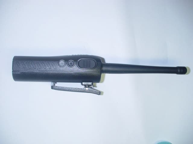
PM3GT10
Dec 08, 2004UHF LMRS TRANSMITTER
Equipment Class
TNF - Licensed Non-Broadcast Transmitter Held to Face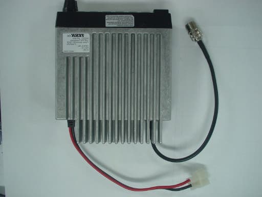
PM3MT900
Nov 28, 2004LAND MOBILE RADIO SERVICE GMRS TRANSMITTER
Equipment Class
TNB - Licensed Non-Broadcast Station Transmitter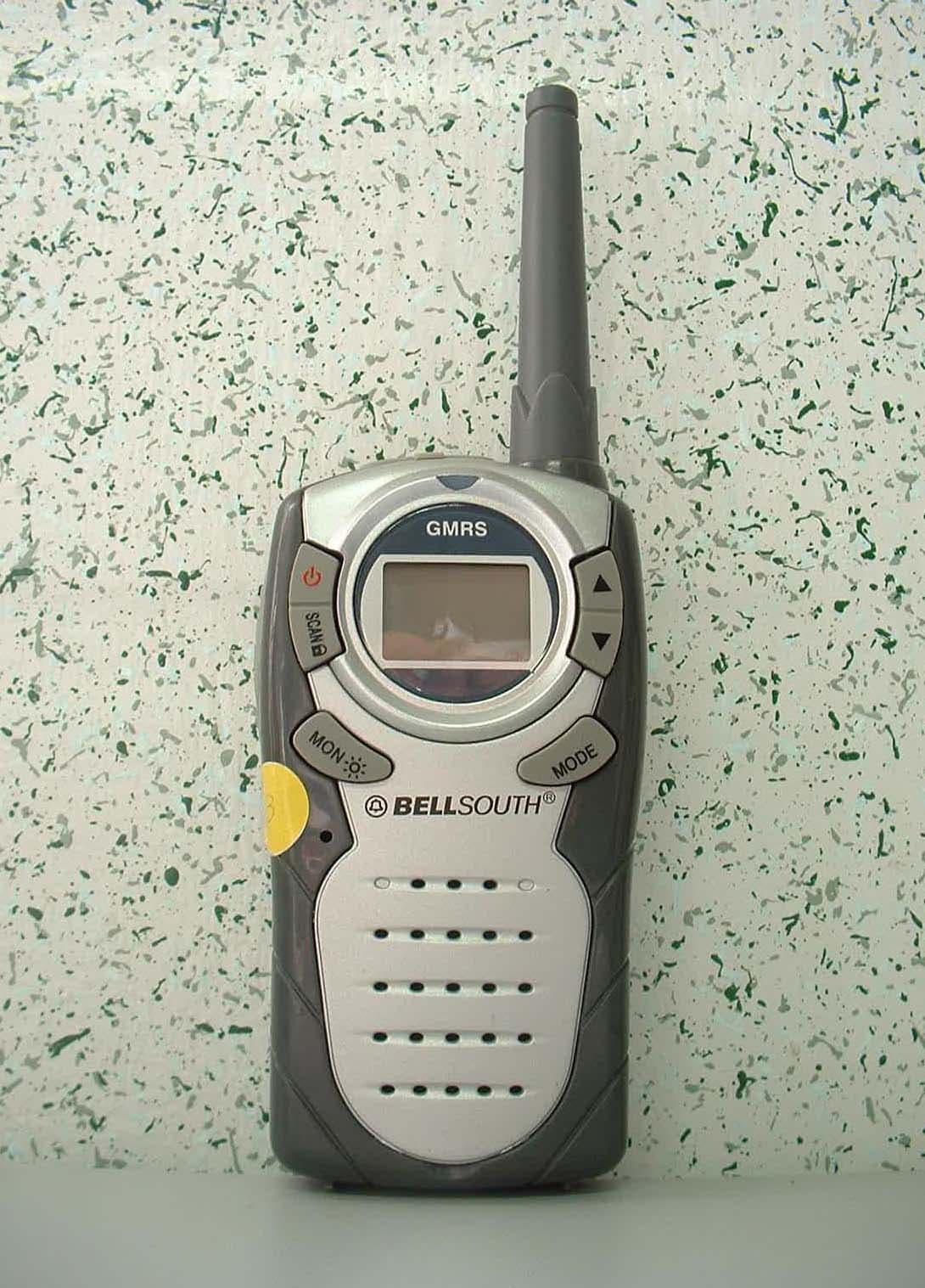
PM3GR5500
Jul 18, 2004GMRS/FRS UHF Transceiver
Equipment Class
FRF - Part 95 Family Radio Face Held Transmitter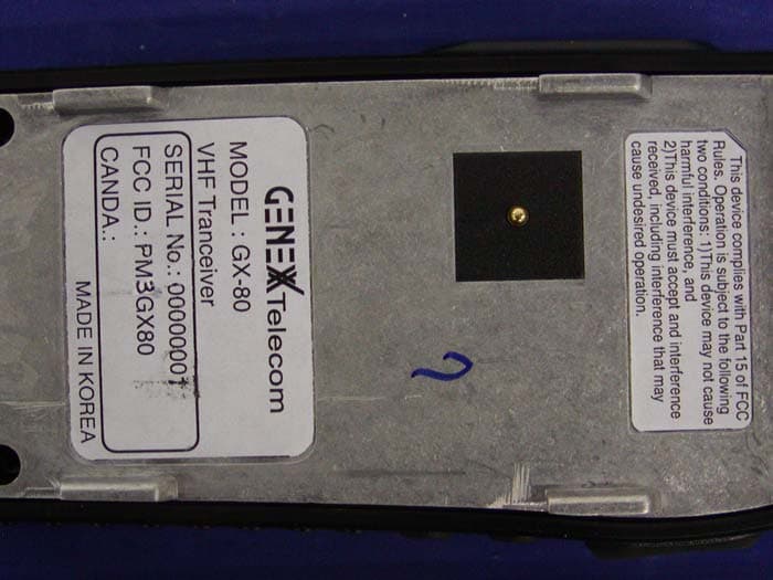
PM3GX80
Jul 01, 2004Transceiver, VHF, PTT
Equipment Class
TNF - Licensed Non-Broadcast Transmitter Held to Face